

Industrial Control (Students guide, 1999, v1.1 )
.pdfExperiment #3: Digital Output Signal Conditioning
DEBUG "!SAVD ON", CR
INPUT 1
INPUT 2
OUTPUT 3
OUTPUT 4
OUTPUT 5
Off CON 1
ON CON 0
OUT3 = Off
OUT4 = Off
OUT5 = OFF
Parts VAR byte
Parts = 0
Start:
GOSUB Plot_data OUT3 = On
DEBUG "!USRS Start conveyor",CR IF IN1 = 1 THEN Process
PAUSE 100 GOTO START
' Save |
data to file |
|
|
'Part Detection |
Switch |
|
|
'Drill |
Depth Switch |
(green) |
|
'Conveyor motor |
relay |
||
'Clamp |
solenoid |
relay |
(yellow) |
'Drill |
press relay |
(red) |
|
'Current sink mode 'Negative logic
'Initialize outputs off
'Plot the status
'Conveyor on
'User status prompt
'If pressed, start "Process"
Process: |
' The process begins |
GOSUB Plot_data |
' Plot the status |
OUT3 = Off |
' Stop conveyor |
DEBUG "!USRS Detected part. Stop conveyor",CR |
|
PAUSE 1000 |
' User status prompt |
|
|
GOSUB Plot_data |
' Plot the status |
OUT4 = On |
' Begin clamping part in place |
DEBUG "!USRS Clamp part.",CR |
' User status prompt |
GOSUB Plot_data |
' Plot the status |
PAUSE 2000 |
' Wait 2 seconds to turn drill on |
Drill_down: |
' Plot the status |
GOSUB Plot_data |
|
OUT5 = ON |
' Turns on drill and drill drops |
DEBUG "!USRS Drill coming down!",CR ' User status prompt |
|
IF IN2 = 1 Then Pull_drill |
' If drill is deep enough, pull drill |
PAUSE 100 |
|
GOTO Drill_down |
|
Pull_drill: |
' Plot the status |
GOSUB Plot_data |
|
OUT5 = OFF |
' Turns off drill and drill retracts |
DEBUG "!USRS Stop Drill and Retract",CR |
|
IF IN2 = 0 Then Drill_up |
' User status prompt |
' Indicates drill is moving up |
|
Industrial Control Version 1.1 •Page 79

Experiment #3: Digital Output Signal Conditioning
PAUSE 100
GOTO Pull_drill |
|
|
Drill_up: |
' Plot |
the status |
GOSUB Plot_data |
||
DEBUG "!USRS Drill coming up!!",CR |
' User status prompt |
|
PAUSE 2000 |
' Pull |
drill for 2 seconds |
Release: |
' Plot |
the status |
GOSUB Plot_data |
||
OUT4 = Off |
' Open |
clamp to release part |
DEBUG "!USRS Clamp released. Conveyor moving.",CR |
|
|
PAUSE 1000 |
'User status prompt |
|
' Wait |
1 seconds |
|
OUT3 = On |
' Conveyor on |
|
IF IN1 = 0 Then Next_part |
|
|
GOTO Release |
|
|
Next_part: |
' Plot |
the status |
GOSUB Plot_data |
||
DEBUG "!USRS Part Complete. Start next cycle",CR |
status prompt |
|
Parts = Parts + 1 |
' User |
|
' Parts counter |
||
PAUSE 1000 |
' Wait |
1 seconds |
DEBUG "Parts completed = ", DEC Parts,CR |
parts count in the List Box |
|
GOTO Start |
' Post |
|
|
|
|
Plot_data:
DEBUG IBIN IN1,BIN IN2,BIN OUT3,BIN OUT4, BIN OUT5,CR
DEBUG DEC Parts,CR |
'Plot |
the digital status. |
'Plot |
analog count |
|
RETURN |
|
|
Page 80 •Industrial Control Version 1.1
Experiment #3: Digital Output Signal Conditioning
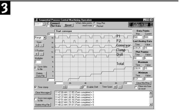
Figure 3.5: Screen Shot of the Sequential Machining Process using StampPlot Lite
Note that the traces appear from top to bottom in the order which they were listed in the Debug digital plot command. Therefore, the top two traces are of the active high pushbuttons IN1 (product in position) and IN2 (depth switch). The next three traces are outputs OUT3 (conveyor), OUT4 (clamp), and OUT5 (drill). Remember that the outputs are wired in the current sink mode. A High is OFF and a Low is ON.
Notice that in the initial setting for the StampPlot Lite interface, “Save data to file” (!SAVD) is ON. During the production run, the data at each sample point is saved into a text file, stampdat.txt. The data includes the time of day and program time that the sample was taken, the sample number, and the analog and digital values at the time of each sample. The data are comma delimited (separated by commas), and therefore, ready to be brought into a variety of spreadsheet or database software packages. Once the data is in the package, it is available for analysis and manipulation. Figure 3.6 represents a portion of the production run data, as it would appear in a Microsoft Excel spreadsheet. The complete file contains 500 samples (rows of data). Figure 3.7 is an Excel graph constructed from the data file.
Industrial Control Version 1.1 •Page 81

Experiment #3: Digital Output Signal Conditioning
Figure 3.6: Sequential Control Production Run (samples only)
|
|
Sample |
Units |
Sample |
Digital |
Time of Day |
Run Time |
number |
Completed |
number |
Status |
11:46:50 AM |
0.21 |
1 |
1 |
1 |
111 |
11:46:50 AM |
0.21 |
2 |
2 |
2 |
11 |
11:46:50 AM |
0.21 |
3 |
3 |
3 |
11 |
11:46:50 AM |
0.21 |
4 |
4 |
4 |
11 |
11:46:50 AM |
0.27 |
5 |
5 |
5 |
11 |
11:46:50 AM |
0.27 |
6 |
6 |
6 |
11 |
11:46:50 AM |
0.27 |
7 |
7 |
7 |
11 |
11:46:50 AM |
0.27 |
8 |
8 |
8 |
11 |
11:46:50 AM |
0.27 |
9 |
9 |
9 |
11 |
11:46:50 AM |
0.27 |
10 |
10 |
10 |
11 |
11:46:50 AM |
0.32 |
11 |
11 |
11 |
11 |
11:46:50 AM |
0.32 |
12 |
12 |
12 |
11 |
11:46:51 AM |
0.43 |
13 |
13 |
13 |
11 |
11:46:51 AM |
0.50 |
14 |
14 |
14 |
11 |
11:46:51 AM |
0.71 |
15 |
15 |
15 |
11 |
11:46:51 AM |
0.98 |
16 |
16 |
16 |
11 |
11:46:51 AM |
1.26 |
17 |
17 |
17 |
11 |
Page 82 •Industrial Control Version 1.1
Experiment #3: Digital Output Signal Conditioning
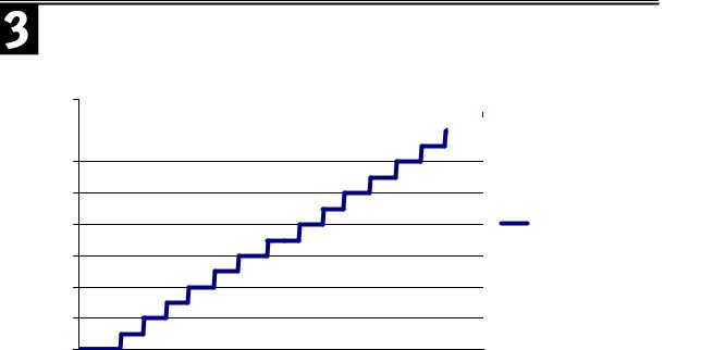
Figure 3.7: Graph of Sequential Control Production Run
Parts Production
16
14 

12
10
8 |
Units Completed |
6
4
2
0
11:46:50 AM 11:46:54 AM 11:47:08 AM 11:47:21 AM 11:47:31 AM 11:47:46 AM 11:47:59 AM 11:48:13 AM 11:48:26 AM 11:48:39 AM 11:48:48 AM 11:49:03 AM 11:49:17 AM 11:49:30 AM 11:49:43 AM 11:49:57 AM 11:50:08 AM 11:50:20 AM 11:50:34 AM 11:50:48 AM
Time of Day
Industrial Control Version 1.1 •Page 83
Experiment #3: Digital Output Signal Conditioning
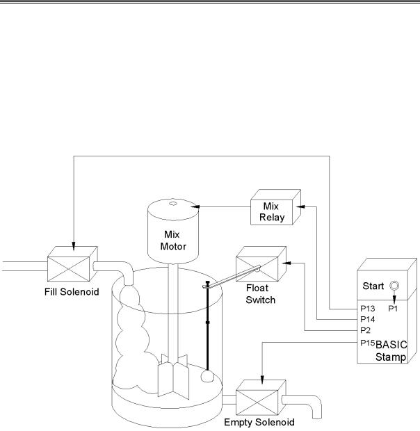
Programming Challenge: Sequential Mixing Operation
A mixing sequence is pictured in Figure 3.8. In this process, an operator momentarily presses a switch to open a valve and begin filling a vat. A mechanical float rises with the liquid level and closes a switch when the vat is full. At this time, the “fill” solenoid is turned off, and a mixer blends the vat contents for 15 seconds. After the mixing period, a solenoid at the bottom of the vat is opened to empty the tank. The mechanical float lowers, opening its switch when the vat is empty. At this point, the “empty” solenoid is turned off and the valve closes. The process is ready for the operator to start another batch.
Figure 3.8: Mixing Sequential Control Process
Assign the following to the BASIC Stamp inputs and outputs to simulate the operation.
Page 84 •Industrial Control Version 1.1

|
|
|
Experiment #3: Digital Output Signal Conditioning |
|
|
|
|
|
|
|
|
Operator pushbutton |
Input P1 |
(N.O. active high) |
|
Float switch |
Input P2 |
(N.O. active high) |
|
Fill Solenoid |
Output P13 |
(red LED) |
|
Mix Solenoid |
Output P14 |
(yellow LED) |
|
Empty Solenoid |
Output P15 |
(green LED) |
|
Construct a flowchart and program the operation.
Exercise #2: Current Boosting the BASIC Stamp
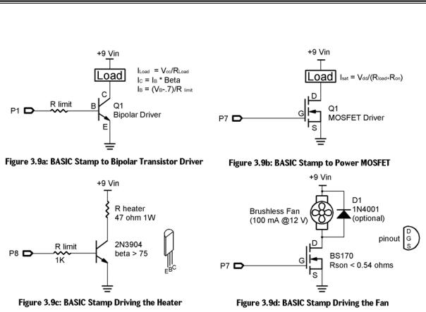
The BASIC Stamp’s output current and/or voltage capability can be increased with the addition of an output transistor. Either the bipolar transistor shown in Figure 3.9a or the power MOSFET transistor in Figure 3.9b can be effective when loads need more power than the BASIC Stamp’s output can deliver. Understanding each of these circuits will be important in future industrial applications.
For this exercise, and upcoming experiments, we have two loads that we wish to drive in this manner. They are a brushless DC fan and a 47-ohm, half-watt resistor. The brushless fan specifications include a full line voltage of +12 V and line current of 100 mA. The resistor will draw approximately 190 mA when powered by the +9 V Vin power supply.
Let’s consider the design of the biplar transistor for driving the 47-ohm resistor. The circuit values should be designed such that a high (+5V) output of the BASIC Stamp drives Q1 into saturation without drawing more current than the BASIC Stamp can source.
Industrial Control Version 1.1 •Page 85
Experiment #3: Digital Output Signal Conditioning
Figure 3.9: Current Boost Transistor Driver Circuits
Circuit component values stem from the load current and voltage requirements. The process of determining minimum component values is as follows: Since Q1 acts as an open collector current sink to the load, the load’s supply voltage is not limited to the BASIC Stamp’s +5-volt supply. If separate supplies are used, however, their common ground lines must be connected. When Q1 is driven into saturation, virtually all of the
supply voltage will be dropped across the load and the load current will be equal to Vsupply/Rload. Q1’s maximum collector current capability must be higher than this load current. The Q1 base current required to yield the
collector current may be calculated by dividing the load current by the “beta” of Q1. IB = IC/bQ1. Given a 20 mA maximum BASIC Stamp output current, a minimum transistor beta may be calculated by rearranging this formula. bQ1(min) = IC/IB. Where IB is the 20 mA maximum BASIC Stamp drive current.
A transistor must be chosen that meets, and preferably exceeds, these minimum requirements. Exceeding the minimum values by 50 to 100% or more would be best. Once the transistor is chosen, an appropriate base-
Page 86 •Industrial Control Version 1.1

Experiment #3: Digital Output Signal Conditioning
limiting resistor value can be determined. This value must allow more base current than that defined by IC/bQ1,
yet less than the 20 mA BASIC Stamp limit. The voltage drop across Rlimit is equal to the +5 V BASIC Stamp output minus the PN junction drop of Q1 (approximately +5V-.7V, or 4.3V).
Following the procedure outlined above, the transistor must handle collector currents of at least 190 mA and have a beta specification greater than 10. Figures 3.9c represents a 2N3904 as Q1. Specifications for the 2N3904 include a collector current capability of 300 mA and a minimum Beta of 75. Added features to the selection of this transistor include that it is very common, it is inexpensive, and it can deliver the load current
without need of a heat sink. Rlimit values were selected based on minimum beta specifications and a desire to keep the BASIC Stamp output current demand well below 20 mA. This 1K-ohm resistor allows approximately 5
mA of base current, which ensures saturation.
Construct the transistor-driver circuits in Figure 3.9c on your Board of Education.
Next, consider the power MOSFET drive circuit in Figure 3.9b. The MOSFET is driven into saturation by applying gate voltage. A positive five volts from the BASIC Stamp’s output is sufficient to place the MOSFET in an “ON” state. When the device is fully saturated, its ON-state resistance (rson) is typically less than 1 ohm. Applying a low (0V) to the gate places the device in cutoff. In this state there is virtually no load current and the MOSFET acts as an open switch.
The power MOSFET is very easy to drive with the BASIC Stamp. A metal oxide (MOS) layer between the source and the gate acts as a very good insulator. The extremely high input impedance provided by this MOS layer means that no gate current is required to control this device. Since no current is required to drive the gate, a single output from the BASIC Stamp can control multiple MOSFETs.
With proper heatsinking, the BS170 can handle load currents up to 5 amps. These features make the power MOSFET very easy to apply in industrial applications such as driving relays, solenoids and small DC motors. It should be noted that these types of loads are inductive. When switching off the load, this inductance can produce a reverse voltage transient that may be damaging to the MOSFET. The diode D1 provides protection for the transistor when driving inductive loads such as these. This diode is not necessary for the small brushless motor used in our experiments. Construct the circuit in Figure 3.9d.
Note: Power MOSFETs, like their CMOS cousins, are suseptable to damage from static discharge and reverse voltage transients. Care should be taken when handling and installing the device. Hold the device by its body, avoid touching its leads, and be sure that the work surface and soldering equipment is properly grounded.
Industrial Control Version 1.1 •Page 87

Experiment #3: Digital Output Signal Conditioning
Test the current-boost drive circuits using the following code. The Debug window will prompt you to make voltage measurements across the transistors and their loads at the proper times.
'Program 3.3: Current-boost for the fan and heater.
Output |
7 |
' |
Output |
for |
Fan drive |
Output |
8 |
' |
Output |
for |
Heater drive |
Loop:
OUT7 = 0
OUT8 = 0
DEBUG "Fan and Heater OFF - Measure the unloaded Vin voltage source.",CR PAUSE 10000
OUT7 = 1
DEBUG "Fan ON – Measure the voltage across the fan.", CR PAUSE 10000
DEBUG "Fan ON – Measure the saturation voltage across the MOSFET.", CR PAUSE 10000
OUT7 = 0
DEBUG "Fan OFF",CR PAUSE 2000
OUT8 = 1
DEBUG "Heater ON – Measure the voltage across the 47-ohm resistor", CR PAUSE 10000
DEBUG "Heater ON – Measure the saturation voltage across the Bipolar.", CR PAUSE 10000
OUT8 = 0
DEBUG "Heater Off",CR PAUSE 2000
GOTO Loop
Record the voltage readings in Table 3.1.
Table 3.1 Transistor Current Boost
Condition |
On-state load |
On-state saturation |
Off-state cutoff |
|
|
|
voltage |
voltage |
voltage |
Bipolar |
Fig. 3.9c |
|
|
|
MOSFET |
Fig. 3.9d |
|
|
|
The fan will be running at full speed, and the resistor will be warming up due to the current flowing through it. Saturation voltages should less than 300 mV. The line voltage Vin is provided by the unregulated 9-volt 300 mA supply. Off-state voltage may measure as high as 14 volts. When the loads are energized, this voltage will drop to around 9 volts.
Page 88 •Industrial Control Version 1.1