

- •Contents
- •Preface
- •Related Documents
- •Typographic and Syntax Conventions
- •Getting Started
- •Starting the Schematic Composer
- •Using the Command Interpreter Window
- •Working with Designs
- •Opening a New Cellview
- •Opening an Existing Cellview
- •Using the Schematic Editor
- •Using the Symbol Editor
- •Making Designs Editable
- •Making Designs Read Only
- •Saving Your Edits
- •Closing Editor Windows
- •Quitting the Schematic Composer
- •Working with Libraries
- •Database Structure
- •Design Libraries
- •Reference Libraries
- •Library Browser
- •Using Menus and the Icon Bar
- •Using Pull-Down Menus
- •Using Pop-Up Menus
- •Using Object-Sensitive Menus (OSMs)
- •Using the Icon Bar
- •Working with Commands
- •Using Command Prompts
- •Canceling a Command
- •Undoing a Command
- •Redoing a Command
- •Displaying a Form
- •Using Form Buttons
- •Using Form Fields
- •Quick Reference Bindkey Charts
- •Quick Reference Bindkey Chart — Schematic Editor
- •Quick Reference Bindkey Chart — Symbol Editor
- •Quick Reference Bindkey Chart — Mouse Buttons
- •Quick Reference Bindkey Chart — General Bindkeys
- •Selecting Objects
- •Dynamic Highlighting
- •Using the Mouse to Select Objects
- •Extending the Selection Area of a Net
- •Selecting One Object
- •Selecting Multiple Objects
- •Selecting Parts of Objects
- •Selecting Wires
- •Selecting a Wire Name and Its Associated Wire Segments
- •Selecting a Pin and Its Associated Wire Segments
- •Selecting an Instance and Its Associated Wire Segments
- •Deselecting Objects
- •Working with Windows
- •Zooming
- •Panning
- •Redrawing a Window
- •Viewing the Same Cell in Two Windows
- •Saving View Area Settings in Memory
- •Restoring View Area Settings
- •Using the Library Browser
- •Accessing and Using the Library Browser
- •Changing the Browser Type Option
- •Using the Library Browser to Initialize Form Fields
- •Using the Component Browser
- •Accessing and Using the Component Browser
- •Changing the Browser Type Option to the Component Browser
- •Opening the Component Browser
- •Opening the Add Instance Form Instead of the Component Browser
- •Listing Components from Several Libraries
- •Changing the Component Browser Display
- •Connectivity with Objects
- •Instance Naming Conventions
- •System-Generated Names
- •Iterated Names
- •Wire Connections and Wire Naming Conventions
- •Wire-to-Wire Connections
- •Wire-to-Pin Connections
- •Wire-by-Name Connections
- •Wire-to-Iterated Instance Connections
- •Global Net Name Connections
- •Multiple-Bit Wire Connections
- •Tapping Multiple Bits of a Bundle
- •Tapping Multiple Bits of a Bus
- •Tapping Wire Intersections by Name
- •Designating Tap Size and Bit Order
- •System-Generated Net Names
- •Multiple-Bit Wire Naming Conventions
- •Using Vector Expressions in Multiple Signals
- •Evaluating Vector Expressions in Multiple-Bit Wire Names
- •Pin Connections and Pin Naming Conventions
- •Hierarchical Pin Names
- •Offsheet Pin Names
- •Bus Pin Names
- •Pin-to-Pin Connections
- •Tapping Pins
- •Naming Single and Multiple Bits Using Patchcords
- •Naming Multiple Nets Using Patchcords
- •Inherited Connections
- •Inherited Connections in a Hierarchy
- •The Syntax of an Inherited Net Expression
- •How Net Expressions Evaluate
- •Sample Net Expression Library
- •Inherited Connections Restrictions
- •Analyzing Net Expression Property Names and Evaluated Names
- •Summary of Naming Conventions
- •Creating Schematics
- •Getting Started with Schematics
- •Adding Instances
- •What Is an Instance?
- •Methods of Adding an Instance to Your Design
- •Adding Instances One by One
- •Adding Instances by Rows and Columns (an Array)
- •Adding Instances Using an Iterative Expression
- •Editing Instance Masters
- •Specifying the View to Use While Placing the Instance
- •Changing the View after an Instance Is Already Placed
- •Renumbering Instances
- •Adding Blocks
- •Adding Blocks
- •Adding Wires and Pins to Blocks
- •Changing the Block Pin Direction Rule
- •Changing the Direction or Name of a Single Block Pin
- •Changing the Names and Directions of Multiple Block Pins
- •Deleting Block Pins
- •Disabling Automatic Block Pin Creation
- •Adding Pins
- •Adding Schematic and Offsheet Pins
- •Showing Pin Connections
- •Adding Wires
- •Adding Narrow or Wide Wires
- •Using Wire Snap and Gravity Options
- •Using Wire Draw, Width, and Route Options
- •Using Wire Flight Lines Option
- •Routing Flight Lines
- •Manipulating Wires with Only the Mouse
- •Adding Wires to Schematic Instance Pins using SKILL
- •Adding Wire Names
- •Naming a Wire
- •Adding Wire Names
- •Adding Multiple Wire Names
- •Verifying Invisible Wire Names
- •Adding Net Expression Labels to Create an Inherited Connection
- •Adding a Net Expression Label to a Wire
- •Adding an Inherited Supply Symbol to a Wire
- •Editing a Net Expression Label
- •Changing the Net Expression Label Display
- •Deleting a Net Expression Label
- •Adding netSet Properties to Create an Inherited Connection
- •Adding a netSet Property to an Instance
- •Modifying a netSet Property
- •Deleting a netSet Property
- •Finding a Net Expression
- •Finding and Replacing a Net Expression
- •Finding Available Properties
- •Viewing the Evaluated Net Names
- •Viewing the Full List of all Hierarchical Paths
- •Checking the Net Expression
- •Adding Solder Dots
- •Adding Solder Dots
- •Deleting Solder Dots
- •Disabling Automatic Solder Dot Creation
- •Changing Solder Dot Size
- •Adding Notes
- •Adding Note Shapes
- •Adding Note Text
- •Importing an ASCII File for Note Text
- •Adding Patchcords
- •Adding Probes
- •Adding Probes to a Net, Pin, or Instance
- •Showing Probe Information
- •Removing Probes from a Net, Pin, or Instance
- •Removing All Probes
- •Saving Probes
- •Loading Probes
- •Creating a Multisheet Schematic
- •Browsing a List of Multisheets
- •Converting a Single-Sheet Schematic to a Multisheet Schematic
- •Adding New Sheets
- •Editing the Title Block
- •Editing the Sheet Border Size and Type
- •Adding Offsheet Pins to Multisheet Schematics
- •Understanding the Index Schematic
- •Going to and from the Index Schematic
- •Repositioning a Schematic within the Sheet Borders
- •Deleting Sheets
- •Reordering Sheets
- •Renumbering Sheets
- •Working with Cross-References
- •Understanding Cross-Reference Zones
- •Understanding Pin Cross-References
- •Understanding Cross-Reference Reports
- •Preparing to Cross-Reference
- •Displaying Cross-References
- •Zooming In to View All Cross-Referenced Pins One by One
- •Viewing Cross-Reference Reports
- •Editing a Cross-Reference Display
- •Controlling the Format String Syntax
- •Customizing the Format String Syntax
- •Customizing Multisheets
- •The Basic Procedure
- •Customizing the Types and Sizes of Sheet Borders
- •Customizing the Cross Reference Options Form
- •Drawing a Customized Sheet Border
- •Drawing a Sheet Border
- •Drawing Sheet Zones
- •Drawing Zone Labels
- •Adding the Sheet Zone Property
- •Adding a Title Block
- •Adding Title Block Values with Normal Labels
- •Adding Title Block Values with NLP and IL Labels
- •Verifying the Label Type
- •Adding Title Block Properties
- •Customizing Pin Cross-References
- •Presetting the Title Block Values
- •Creating Symbols
- •Setting Grid Options
- •Importing Symbols
- •Creating New Symbols
- •Drawing Lines
- •Drawing Rectangles
- •Drawing Polygons
- •Drawing Circles
- •Drawing Ellipses
- •Drawing Arcs
- •Adding Pins as Graphic Images
- •Adding Pins as Instances
- •Creating Custom Pins as Graphic Images
- •Duplicating Pin Figures in the Symbol Master
- •Making the Custom Pin Name Visible
- •Adding a Selection Box
- •Adding Labels
- •Adding a Normal Label
- •Adding an NLP Label
- •Adding an IL Label
- •Adding Note Text and Note Shapes
- •Adding a Net Expression Label
- •Setting the Symbol Origin
- •Creating Symbol Cellviews Using Generators
- •Automatically Creating Cellviews
- •Features of Creating Cellviews
- •Automatically Creating a Cellview from Another Cellview
- •Replacing an Existing Symbol Cellview
- •Modifying an Existing Symbol Cellview
- •Examples of Replacing and Modifying Pins on a Symbol
- •Automatically Creating a Cellview from a Pin List
- •Automatically Creating a Cellview from an Instance
- •Editing Symbol Generation Options
- •Adding, Changing, and Reordering Pin Names
- •Editing Pin Attributes
- •Loading and Saving a TSG Template File
- •Editing Symbol Attributes
- •Editing Symbol Labels
- •Creating a New Label
- •Deleting Labels
- •Modifying Label Attributes
- •Editing Properties
- •Creating a New Property
- •Deleting Properties
- •Modifying Property Attributes
- •Specifying Symbol Generator Pin Sorting
- •Editing Objects
- •Using Direct Manipulation
- •Direct Manipulation Operations
- •Turning Off Direct Manipulation
- •Undoing and Redoing an Edit
- •Changing the Undo Limit
- •Stretching
- •Stretching with the Schematic Editor
- •Stretching with the Symbol Editor
- •Stretching with Direct Manipulation
- •Stretching with Bindkeys
- •Copying
- •Copying Single Objects
- •Copying Arrays of Objects
- •Copying Across Cellviews
- •Copying with Direct Manipulation
- •Copying with Bindkeys
- •Moving
- •Moving Objects
- •Moving with Direct Manipulation
- •Moving with Bindkeys
- •Deleting
- •Deleting Preselected Objects
- •Deleting Postselected Objects
- •Deleting Sheet Borders
- •Rotating
- •Rotating Preselected Objects
- •Rotating Postselected Objects
- •Rotating with Direct Manipulation
- •Rotating with Bindkeys
- •Discarding Edits
- •Alternating Symbol Views
- •Changing the View of a Preselected Object
- •Changing the View of a Postselected Object
- •Toggling Objects
- •Toggling Pin Direction Options
- •Toggling Wire Draw Mode Options
- •Toggling Instance Symbol View Options
- •Saving the Current Label Display File
- •Loading the Current Label Display File
- •Attaching the Label Display File to the Library
- •Detaching the Label Display File from the Library
- •Setting the Simulation Data Directory
- •Editing Properties
- •Using Command Shortcuts
- •Search String Wildcards
- •Replacing Properties
- •Replacing String-Tagged Characters
- •Selecting Objects to Edit
- •Using Modal (Repeating) Commands
- •Selecting Objects by Filtering
- •Selecting Objects Automatically by Type
- •Selecting Objects by Property
- •Adding a Property Name to the Search List
- •Selecting Objects by Filtering
- •Object and Cellview Property Types and Values
- •Editing Object Properties
- •Applying Edits to Objects and Displaying Object Types
- •Adding Object Properties
- •Deleting Object Properties
- •Modifying Object Properties
- •Editing Instance and Block Properties
- •Editing Pin Properties
- •Designating the Order of Pins
- •Copying a Pin Order from Another Cellview
- •Resolving Pin Order Mismatch
- •Verifying Pin Order
- •Editing Pin Name Properties
- •Editing Wire Properties
- •Editing Wire Name Properties
- •Editing Instance Pin Properties on an Instance of a Block
- •Editing Label Properties
- •Resetting Invisible Labels
- •Editing netSet Properties
- •Editing Note Text Properties
- •Editing Note Shape Properties
- •Editing Symbol Shape Properties
- •Editing Symbol Pin Properties
- •Editing Symbol Label Properties
- •Editing Symbol Selection Box Properties
- •Passing Parameters in a Design
- •Editing Cellview Properties
- •Adding Cellview Properties
- •Deleting Cellview Properties
- •Modifying Cellview Properties
- •Editing VHDL Properties
- •Adding VHDL Properties
- •Deleting VHDL Properties
- •Modifying VHDL Properties
- •Setting the Tool Filter
- •About the Design Hierarchy
- •Exploring the Design Hierarchy
- •Top-Level Schematic View
- •Middle-Level Schematic View
- •Lower-Level Design Hierarchy
- •About the Hierarchy Editor
- •Traversing a Design Hierarchy
- •Descending Using the Descend Command
- •Editing an Instance in Place
- •Descending Using the View Name List
- •Setting the View Precedence Order
- •Returning Up the Design Hierarchy
- •Using OSMs to Traverse the Design Hierarchy
- •Using Bindkeys to Traverse the Design Hierarchy
- •Displaying the Current Hierarchical Scope
- •About the Hierarchy Editor within the Schematic Composer
- •Opening a Hierarchy Editor Menu within the Schematic Composer
- •Setting Instance Bindings
- •Building a New Inherited View List
- •Showing Views Found
- •Checking Designs
- •Features of the Check Commands
- •Setting the Check Options
- •Setting User Preferences
- •Setting Schematic Rule Checks
- •Checking a Design
- •Checking and Saving a Design
- •Checking the Current Cellview
- •Checking a Design Hierarchy
- •Checking Multisheet Schematics
- •Checking a Label Attachment
- •Cross-View Checking
- •Bypassing Checks
- •Bypassing Floating Pin Checks
- •Bypassing Unconnected Wire Checks
- •Resolving Check Errors
- •Finding Errors and Warnings in a Design
- •Mapping an Error Message to a Marker
- •Managing the Error Message List
- •Assigning an ignoreCheck Property
- •Suppressing Message Displays
- •Deleting an ignoreCheck Property
- •Deleting All ignoreCheck Properties
- •Deleting Individual Markers
- •Deleting All Markers
- •Monitoring a Verilog or VHDL Simulation State
- •Using Cross Selection
- •Opening an SHM Database
- •Displaying the Simulation State of Wires and Pins
- •Setting a Time Value for Displaying Signal Results
- •Setting the Time Scale
- •Setting the Display Radius
- •Synchronizing with Simulation at Breakpoint
- •Closing the SHM Database
- •Plotting Designs
- •Setting Up System Options to Plot
- •Setting Up Printer Options to Use Various Paper Sizes
- •Plotting a Design
- •Plotting a Library
- •Plotting a Cellview
- •Plotting Part of a Schematic
- •Plotting Without a Header Page for Every Session
- •Adding Notes to a Plot
- •Setting Plot Options
- •Plotting a Color Schematic in Black and White
- •Changing the Background Color of a Schematic Window
- •Using a Plot Template File
- •Creating a Plot Template File
- •Loading a Plot Template File
- •Creating a Default Plot Template File
- •Checking the Queue Status
- •Canceling a Plot Job
- •Setting Schematic Composer Options
- •Overview of Schematic Composer Options
- •Changing User Preferences
- •Minimizing Mouse Clicks
- •Changing the Default Display Setting for Command Option Forms
- •Saving the Current Window Setup
- •Restoring a Saved Window Setup
- •Viewing Bindkey Settings
- •Changing Browser and CIW Preferences
- •Customizing Editor Options
- •Canceling the Modal (Repeat) Command Option
- •Changing Display Options
- •Selecting Objects Using the Filter Option
- •Setting Plot Options
- •Setting Schematic Check Options and Rules
- •Setting the Tool Filter
- •Saving Form Field Default Settings
- •Loading Form Field Default Settings
- •Customizing the Schematic Composer
- •Customizing Pull-Down and Pop-Up Menus
- •Sample Menu File
- •Customizing Object-Sensitive Menus
- •Example of Customizing the Instance OSM
- •Customizing the Icon Bar
- •Positioning Icons and Turning Off Icon Names
- •Changing the Contents of the Icon Bar
- •Changing the Display of the Icon Bar
- •Understanding Initialization and Setup Files
- •Converting a Schematic from a 0.125 Grid to a 0.1 Grid
- •Customizing Bindkeys
- •Locating the schBindKeys.il Bindkey File
- •Locating Your Installation Directory
- •Loading Your Customized Bindkey File
- •Loading the Cadence-Supplied Bindkey File
- •Customizing Global Editor Variables for Form Fields
- •Schematic Editor Variables
- •Symbol Editor Variables
- •Symbol Generation (tsg) Variables
- •HDL (Verilog, SpectreHDL, and VerilogA) Variables
- •AMS Netlisting Variables
- •Block Pin Direction Rule Variable
- •Block Sample Sizes Variable
- •View Name Exclusion Variable
- •Schematic Pin Types Variable
- •Plot Template File Variable
- •Property Filter Variable
- •Schematic Rule Checker Variable
- •Properties for Find Variable
- •Multisheet Masters Variable
- •Simulation Probe Masters Variable
- •View Name Masters Variable
- •View Master Options Variable
- •Zone Formats Variable
- •Symbol Label Variables
- •Symbol Pin Masters Variable
- •Customizing Text-to-Symbol Generator (TSG) Variables for Form Fields
- •Pin Master Connections Variable
- •Symbol Pin Characteristics Variable
- •Template Masters Variables
- •Customizing HDL Variables for Form Fields
- •Edit After Error Variable
- •Update Symbol After Edit Variable
- •Cross View Check Variable
- •Cross View String Variable
- •Printing Variable
- •Verbose Variable
- •No Hierarchy Variable
- •Net to Port Variable
- •Environment Variables
- •Overview of Environment Variables
- •Schematic Editor Environment Variables File
- •Window Environment Variables
- •schDisplayDepth
- •schDrawAxesOn
- •schDynamicHilightOn
- •schGridMultiple
- •schGridSpacing
- •schGridType
- •schMaxDragFig
- •schPathType
- •schShowDirectConnects
- •schShowLabelOrigin
- •schSnapSpacing
- •schWindowBBox
- •symDisplayDepth
- •symDrawAxesOn
- •symDynamicHilightOn
- •symGridMultiple
- •symGridSpacing
- •symGridType
- •symMaxDragFig
- •symPathType
- •symShowDirectConnects
- •symShowLabelOrigin
- •symSnapSpacing
- •symWindowBBox
- •viewNameList
- •Schematic Environment Variables
- •autoDot
- •blockDirRules
- •broadcast
- •browserType
- •checkAlways
- •checkBeepOn
- •checkHierSave
- •checkSymTime
- •compBackTrace
- •condOp
- •createCvOptions
- •createInstResetCDF
- •createInstShowCDF
- •createLabelFontHeight
- •createLabelFontStyle
- •createLabelHorzOffset
- •createLabelHorzPosition
- •createLabelHorzRotation
- •createLabelJustify
- •createLabelOffsetMode
- •createLabelVertOffset
- •createLabelVertPosition
- •createLabelVertRotation
- •cvDisplay
- •defaultsFile
- •defWideWireWidth
- •descendSheet
- •descendTarget
- •dotOverlap
- •drawMode
- •drawModeRoute
- •echoToCIW
- •editPropShowCDF
- •editPropShowSystem
- •editPropShowUser
- •gravityOn
- •libList
- •markerSeverity
- •markerShowIgnore
- •markerZoom
- •maxLabelOffsetUU
- •minMarkerSize
- •modalCommands
- •netExprDisplay
- •netNameMethod
- •netNameRangeDescend
- •netNameSeparator
- •noteFontHeight
- •noteFontStyle
- •noteJustify
- •noteShape
- •noteShapeLineStyle
- •pinBackTrace
- •pinNameSeed
- •pinRefDuplicates
- •pinRefFormat
- •pinRefSorting
- •replSaveChanges
- •runSRC
- •runVIC
- •saveAction
- •schematicAreaPartialSelect
- •schematicSelectFilter
- •sensitiveMenu
- •shapeLineType
- •shapeLineWidth
- •simProbeFormat
- •simProbeType
- •snapEnabled
- •spanLib
- •srcConnByName
- •srcFloatingBIDIR
- •srcFloatingInput
- •srcFloatingIO
- •srcFloatingNets
- •srcFloatingOutput
- •srcInheritedConnCheck
- •srcInstNameExpr
- •srcInstNameSyntax
- •srcInstOverlap
- •srcInstOverlapValue
- •srcMaxLabelOffset
- •srcNameCollision
- •srcNetNameExpr
- •srcNetNameSyntax
- •srcNoOverrideNet
- •srcOffsheetConnCheck
- •srcPinNetCollision
- •srcShortedOutputs
- •srcSolderOnCrossover
- •srcTermNameExpr
- •srcTermNameSyntax
- •srcUnconnectedWires
- •srcVerilogSyntax
- •srcVHDLSyntax
- •ssgSortPins
- •statusBanner
- •statusBannerXY
- •stickyWireLabelRange
- •symbolAreaPartialSelect
- •symbolLabelChoiceText
- •symbolLabelFontHeight
- •symbolLabelFontStyle
- •symbolLabelJustify
- •symbolLabelType
- •symbolPinFlatten
- •symbolPinIncrCount
- •symbolPinLocate
- •symbolPinUsage
- •symbolSelectFilter
- •symbolShape
- •symbolShapeFillStyle
- •transToSheetType
- •tsgTemplateType
- •updateConn
- •vicExactPinMatch
- •vicInheritedPins
- •vicInheritedPinsMatch
- •vicSeverity
- •vicViewList
- •wireBackTrace
- •zoomOutButton
- •Text-to-Symbol Generator
- •Symbol Shape Generated by TSG
- •TSG Symbol Description File
- •TSG Template File
- •Clock and Negation Indicators
- •Backannotation
- •Simple File Example
- •Complex File Example
- •Extended File Example
- •TSG Symbol Description File Structure
- •Basic File Structure
- •Data Types
- •Using TSG Constructs
- •Input Pin
- •Output Pin
- •Executing TSG
- •TSG Processing Order
- •Creating Symbols Automatically from a Schematic
- •Terms and Conventions
- •Library Command File
- •Running the Symbol and Simulation Library Generator
- •Running the Symbol and Simulation Library Generator in the Cadence Graphic Environment
- •Running the Symbol and Simulation Library Generator in the Cadence Nongraphic Environment
- •Library Management Commands
- •lmCheckTerm
- •lmCheckView
- •lmCloseLib
- •lmDefCell
- •lmDefTermProp
- •lmDefViewProp
- •lmDeleteTermProp
- •lmDeleteViewProp
- •lmGetValue
- •lmLoadData
- •lmOpenLib
- •lmPrintLibTermProp
- •lmPrintLibViewProp
- •lmPrintTerm
- •lmPrintTermProp
- •lmPrintViewProp
- •lmReset
- •lmSimView
- •simRep
- •Variables That Control Command Execution
- •Properties That Modify Values
- •Sample Library Command File
- •Configuring and Using Kanji Notes
- •Overview
- •Installing the Required Files
- •Uncompressing the Files
- •Modifying the Schematic Editor Menu File
- •Setting the Environment Variable
- •Modifying the Data Registry File
- •Using Kanji Notes
- •Formats, Files, and Views
- •Adding a New Note
- •Generating a Symbol from an Existing File
- •Generating a Symbol from a New File
- •Editing an Existing Note
- •Limitations
- •Known Problems
- •schHiCreateKanjiSymbol
- •Form Descriptions
- •Add Block Form
- •Add Custom Pin Form
- •Add Generic Form – VHDL Properties
- •Add Instance Form
- •Add Kanji Note Form
- •Add Net Expression Form
- •Add New Property to Find Form
- •Add New Property to Replace Form
- •Add New Property for Search Form
- •Add Note Shape Form – Arc
- •Add Note Shape Form – Circle
- •Add Note Shape Form – Ellipse
- •Add Note Shape Form – Line
- •Add Note Shape Form – Polygon
- •Add Note Shape Form – Rectangle
- •Add Note Text Form
- •Add Pin Form – Schematic
- •Add Pin Form – Symbol
- •Add Property Form – Edit Object Properties
- •Add Selection Box Form
- •Add Simulation Monitor Form
- •Add Symbol Label Form
- •Add Symbol Shape Form – Arc
- •Add Symbol Shape Form – Circle
- •Add Symbol Shape Form – Ellipse
- •Add Symbol Shape Form – Line
- •Add Symbol Shape Form – Polygon
- •Add Symbol Shape Form – Rectangle
- •Add Wire Form
- •Add Wire Name Form
- •Build Inherited View List Form
- •Cellview From Cellview Form
- •Cellview From Instance Form
- •Cellview From Pin List Form
- •Cellviews with Evaluated Net Expression Name Form
- •Change Sheet Border Size Form
- •Check Hierarchy Form
- •Component Browser Form
- •Component Browser Preferences Form
- •Copy Form
- •Create Cellview Dialog Box – Replace or Modify
- •Create Schematic Form
- •Create Schematic Sheet Form
- •Cross Reference Options Form
- •Cross-View Checker Form
- •Delete All Markers Form
- •Delete Generic Form – VHDL Properties
- •Delete Property Form – Edit Object Properties
- •Delete Schematic Sheet Form
- •Descend Form – Descend Options
- •Descend Form – Iterated Instance
- •Descend Form – Multisheet
- •Descend Form – Noniterated Instance
- •Display Options Form
- •Edit Cellview Properties Form
- •Edit Component Display Form
- •Edit Object Properties Form – Basic
- •Edit Object Properties Form – Instance and Block
- •Edit Object Properties Form – Instance Pin
- •Edit Object Properties Form – Label
- •Edit Object Properties Form – Master Property
- •Edit Object Properties Form – Net Expression
- •Edit Object Properties Form – Note Shapes
- •Edit Object Properties Form – Note Text
- •Edit Object Properties Form – Other Object
- •Edit Object Properties Form – Pin
- •Edit Object Properties Form – Pin Name
- •Edit Object Properties Form – Selection Box
- •Edit Object Properties Form – Symbol Label
- •Edit Object Properties Form – Symbol Pin
- •Edit Object Properties Form – Symbol Shape
- •Edit Object Properties Form – Wire Name
- •Edit Object Properties Form – Wire Segment
- •Edit Pin Order Form
- •Edit Schematic Sheet Number Form
- •Editor Options Form
- •Find Marker Form
- •Go To Pin Form
- •Go To Sheet Form
- •Import Symbol Form
- •Left, Right, Top, Bottom Pin Attributes Form
- •Load Label Display Form
- •Load Schematic Defaults Form
- •Modify Generic Form – VHDL Properties
- •Modify Property Form – Edit Object Properties
- •Move Form
- •Net Expression Available Property Names Form
- •Net Expression Evaluated Names Form
- •Occurrence Paths to Evaluated Name Form
- •Open Simulation Data Form
- •Plot Options Form
- •Renumber Instances Form
- •Reset Invisible Labels Form
- •Rotate Form
- •Route Flight Line Form
- •Save Label Display Form
- •Save Schematic Defaults Form
- •Save Schematics with Errors Form
- •Schematic Check Options Form
- •Schematic Find and Symbol Find Forms
- •Schematic Replace and Symbol Replace Forms
- •Schematic Select All Form
- •Schematic Select By Property Form
- •Schematic Selection Filter Form
- •Schematic Title Block Properties Form
- •Set Instance Binding Form
- •Set Label Display Simulation Data Directory Form
- •Set Radix Form
- •Set Time Form
- •Setup Schematic Rules Checks Form
- •Show Label Form
- •Show Views Found Form
- •Stretch Form – Schematic Editor
- •Stretch Form – Symbol Editor
- •Submit Plot Form
- •Symbol Generation Options Form
- •Symbol Select All Form
- •Symbol Select By Property Form
- •Symbol Selection Filter Form
- •Synchronization Form
- •Time Scale Form
- •VHDL Properties Form
- •Glossary

Virtuoso Schematic Composer User Guide
Understanding Connectivity and Naming Conventions
You can repeat a single signal name, a group of signal names, or a vector term any number of times in the wire name by placing a prefix repeat operator<*n> in front of the name, where n is a positive integer that defines the number of times to repeat each bit in the vector term.
■Use the prefix repeat operator<*n> to repeat a single-signal name. The following equivalent wire names both name the same four-bit wire:
<*2>A,B,C
A,A,B,C
■Use the prefix repeat operator<*n> and parentheses to repeat a group of signal names.
The following two wire names are equivalent:
<*2>(A,B),C
A,B,A,B,C
■Use combinations of the prefix repeat operator<*n> and parentheses to nest parenthetical expressions to any required depth. The editor expands nested expressions from the innermost expression outward. For example, a name with the expression
<*2>(A,<*2>(X,Y)),B expands to A,X,Y,X,Y,A,X,Y,X,Y,B.
Using Suffix Repeat Operators in Multiple-Bit Wire Names
A multiple-bit wire name can be a bundle, a bus, or a combination of the two. You can improve readability in your designs by shortening multiple-bit wire names using vector expressions.
A suffix repeat operator is a number,<*n>, after a vector term, where n is a positive integer that defines the number of times to repeat each bit in the vector term.
■Use the suffix repeat operator<*n> to repeat each bit in a group of bit names before expanding the vector term. For example, the following three names all describe the same six-bit wire:
A<0:2*2>
A<0*2,1*2,2*2>
A<0,0,1,1,2,2>
■Use the suffix repeat operator<*n> and parentheses to repeat the sequence of bit names. In this case, the vector term is expanded before the bits are repeated. The following names all describe the same six-bit wire:
A<(0:2)*2>
A<0:2,0:2>
A<0,1,2,0,1,2>
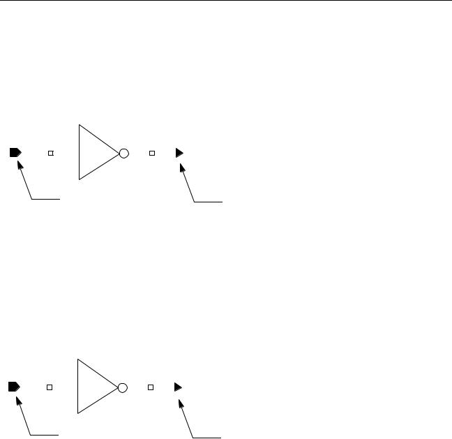
Pin Connections and Pin Naming Conventions
A pin name consists of a string of printable characters. You must observe the rules for reserved characters.
October 2002 |
107 |
Product Version 5.0 |

Virtuoso Schematic Composer User Guide
Understanding Connectivity and Naming Conventions
You can name pins in a design
■To declare which nets in the schematic are connected to a higher level of the design hierarchy
■To declare which nets span across sheets in a multisheet schematic
This section describes the following pin connections and naming conventions:
■Hierarchical Pin Names on page 109
■Offsheet Pin Names on page 109
■Bus Pin Names on page 109
■Pin-to-Pin Connections on page 110
■Tapping Pins on page 110
October 2002 |
108 |
Product Version 5.0 |
Virtuoso Schematic Composer User Guide
Understanding Connectivity and Naming Conventions
Hierarchical Pin Names
If you are designing a multisheet schematic, your sheets contain hierarchical pins and offsheet pins.
Hierarchical pins are pins that also appear on the symbol of the design. The hierarchical pins from each sheet become the hierarchical pins of the multisheet.
A<0:7> |
IO<0:7> |
OUT2<0:7> |
|
|
|
|
|
|
|
|
|
|
Hierarchical pin |
|
|
Offsheet pin |
||
Offsheet Pin Names
Offsheet pins connect signals across the sheets of a multisheet schematic only. Use the same name for the offsheet pins on each sheet.
If you want a signal to appear on a multiple sheet that is also exported by a hierarchical pin, place a hierarchial pin for the first usage and offsheet pins on other sheets. Do not place more than one hierarchical pin with the same name in a multisheet design.
A<0:7> |
IO<0:7> |
OUT2<0:7> |
|
|
|
|
|
|
|
|
|
|
Hierarchical pin |
|
|
Offsheet pin |
||
Bus Pin Names
Use a base name with a vector expression. For example, IN<16:10:2> expands to these four pins: IN<16>, IN<14>, IN<12>, and IN<10>.
October 2002 |
109 |
Product Version 5.0 |
Virtuoso Schematic Composer User Guide
Understanding Connectivity and Naming Conventions
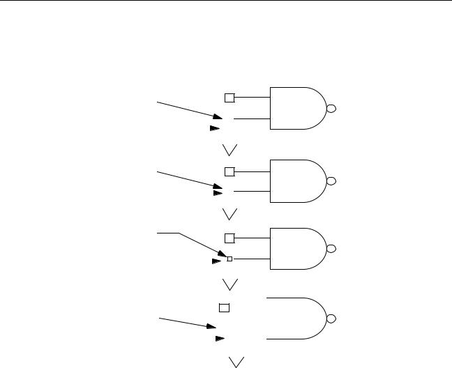
Pin-to-Pin Connections
A direct connection between two instance pins without an intermediate wire is called a pin-to- pin connection. There are four ways to make pin-to-pin connections:
Pin 1
Pins overlap partially.
|
Pin 2 |
|
|
|
|
|
|
|
|
|
|
|
|
|
|
|
|
|
|
|
|
|
|
|
|
|
|
|
|
|
|
|
|
||
|
|
|
|
|
|
|
|
|
|
|
|||||||
|
|
|
|
|
|
|
|
|
|
|
|
|
|
|
|
|
|
|
|
|
|
|
|
|
|
|
|
|
|
|
|
|
|
|
|
Pins overlap entirely. |
Pin 1 |
|
|
|
|
|
|||||||||||
|
|
|
|
|
|||||||||||||
Pin 2 |
|
|
|
|
|
|
|
|
|
|
|
|
|
|
|
|
|
|
|
|
|
|
|
|
|
|
|
|
|
|
|
|
|||
|
|
|
|
|
|
|
|||||||||||
|
|
|
|
|
|
|
|
|
|||||||||
|
|
|
|
|
|
|
|
|
|
|
|
|
|
|
|
|
|
Pin is contained within |
Pin 1 |
|
|
|
|
|
|||||||||||
|
|
|
|
|
|||||||||||||
|
|
|
|
|
|
|
|
|
|
|
|
|
|
|
|
|
|
a pin. |
|
|
|
|
|
|
|
|
|
|
|
|
|
|
|
|
|
|
Pin 2 |
|
|
|
|
|
|
|
|
|
|
|
|
|
|
|
|
|
|
|
|
|
|
|
|
|
|
|
|
|
|
|
|
||
Pins touch each other. |
Pin 1 |
|
|
|
|
|
|
|
|
||||||||
|
|
|
|
|
|
|
|||||||||||
|
|
|
|
|
|
|
|
|
|||||||||
|
|
|
|
|
|
|
|
|
|||||||||
|
|
|
|
|
|
|
|||||||||||
|
|
|
|
|
|
|
|||||||||||
|
|
|
|
|
|
|
|
|
|
|
|
|
|
|
|
|
|
|
Pin 2 |
|
|
|
|
|
|
|
|
|
|
|
|
|
|
|
|
|
|
|
|
|
|
|
|
|
|
|
|||||||
|
|
|
|
|
|
|
|
|
|
|
|||||||
|
|
|
|
|
|
|
|
|
|
|
|
|
|
|
|
||
|
|
|
|
|
|
|
|
|
|
|
|
|
|
|
|
|
|
|
|
|
|
|
|
|
|
|
|
|
|
|
|
|
|
|
|
Tapping Pins
You cannot draw a tap directly from an instance pin.
To tap a multibit connection to an instance pin, you must attach a wire named with a bus name to the instance pin. You can then draw taps from the named bus.
If a schematic pin has a bus name, you can draw a tap directly from the pin using a vector expression to name a wire that intersects with the pin.
October 2002 |
110 |
Product Version 5.0 |
Virtuoso Schematic Composer User Guide
Understanding Connectivity and Naming Conventions
The following figure shows how to tap pins in a design.
Symbol pins
|
I1<0:3> |
|
|
<7:4> A |
Y |
I4<0:3> |
|
INPUT |
inv |
OUTPUT |
|
<7:0> |
A |
<0:3> |
|
|
Y |
||
|
|
B |
|
<3:0> |
|
nand2 |
|
|
|
|
Hierarchical pin |
Wire named |
Hierarchical pin |
|
OUTPUT<0:3> |
|
In the example above, the wire named <7:4> is a tap of the schematic pin named INPUT<7:0> and connects a four-bit bus called INPUT<7:4> to the input of the inverter (an iterated instance).
The wire named <3:0> is also a tap of the INPUT<7:0> pin and connects a four-bit bus called INPUT<3:0> to the input of the NAND2 gate (also an iterated instance).
If you do not apply a name to a net that is attached to a pin, the editor gives the net the same name as the pin. For example, the wire that connects the output of the NAND2 gate to the
OUTPUT<0:3> pin is called OUTPUT<0:3>.
Patchcord Connections and Patchcord Naming
Conventions
The schPatchExpr connection expression (value) for patchcords has the following form:
srcVectorExpression = dstVectorExpression
0=0
A |
B |
October 2002 |
111 |
Product Version 5.0 |