

Chapter 9 SCXI—Signal Conditioning
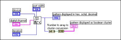
Digital Input Application Example
To input digital signals through an SCXI chassis, you can use the
SCXI-1162 and SCXI-1162HV modules and the Easy Digital VI,
Read from Digital Port, as shown in Figure 9-13.
Figure 9-13. Inputting Digital Signals through an SCXI Chassis Using Easy Digital VIs
If you configure channels using the DAQ Channel Wizard, digital channel can consist of a digital channel name. The channel name can refer to either a port or a line in a port. You do not need to specify device, line, or port width, as these inputs are not used by LabVIEW if a channel name is specified in digital channel.
As an alternative, digital channel can be expressed in the scx!mdy!0 format, where you are trying to input from the digital input module on slot y of chassis x. The last identifier is always port 0, because the whole module is considered one port. In this example, you also must specify device and port width. The port width should be the number of lines in a port on your SCXI module if you are operating in multiplexed mode. For the SCXI-1162 and SCXI-1162HV, the port width is 32 lines. If you are operating in parallel mode, the port width should be the number of lines on your DAQ device. The DIO-32F/DIO-32HS/6533 device can access all 32 lines of the SCXI modules at once by using the SCXI-1348 cable assembly. The DIO-24 and the DIO-96 devices can access only the first 24 lines of these modules when configured in parallel mode. For the fastest performance in parallel mode, you can use the appropriate onboard port numbers instead of the SCXI channel string syntax.
Use the iteration input to optimize your digital operation. When iteration is 0 (default), LabVIEW calls the DIO Port Config VI (an Advanced VI) to configure the port. If iteration is greater than zero, LabVIEW bypasses reconfiguration and remembers the last configuration, which improves performance. You can wire this input to an iteration terminal of a loop. With the DIO-24 and DIO-96 devices, every time you call the DIO Port Config VI, the digital line values are reset to default values. If you want
© National Instruments Corporation |
9-31 |
LabVIEW Measurements Manual |
Chapter 9 SCXI—Signal Conditioning
to maintain the integrity of the digital values from one loop iteration to another, do not set iteration to 0 except for the first iteration of the loop.
Refer to the SCXI-1162HV Digital Input VI in the examples\daq\ scxi\scxi1162.llb for an example of SCXI digital input. Even though this VI uses Advanced VIs, it is functionally equivalent to the Easy I/O Digital VI, Read from Digital Port.
Note The DIO Port Config VI resets output lines on adjacent ports on the same 8255 chip for DIO-24, DIO-96, and Lab and 1200 Series devices.
Note If you also are using SCXI analog input modules, make sure your cabling DAQ device is cabled to one of them.
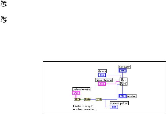
Digital Output Application Example
To output digital signals through an SCXI chassis, you can use the SCXI-1160, SCXI-1161, SCXI-1163, and SCXI-1163R modules and the digital Easy Digital VI, Write to Digital Port, as shown in Figure 9-14.
Figure 9-14. Outputting Digital Signals through an SCXI Chassis Using Easy Digital VIs
If you configure channels using the DAQ Channel Wizard, digital channel can consist of a digital channel name. The channel name can refer to either a port or a line in a port. You do not need to specify device, line, or port width, as these inputs are not used by LabVIEW if a channel name is specified in digital channel.
As an alternative, digital channel can be expressed in the scx!mdy!0 format, where you are trying to output from the digital output module on slot y of chassis x. The last identifier is always port 0, because the whole module is considered one port. In this case, you also must specify device
LabVIEW Measurements Manual |
9-32 |
www.ni.com |
Chapter 9 SCXI—Signal Conditioning
and port width. The port width should be the number of lines on your SCXI module if you are operating in multiplexed mode. The SCXI-1160 has 16 relays, the SCXI-1161 has eight relays, and the SCXI-1163/1163R have 32 relays. You can not use the SCXI-1160 or SCXI-1161 in parallel mode. For the SCXI-1163/1163R the port width in parallel mode should be the number of lines on your DAQ device or SCXI-1200 module. The 6533 device can access all 32 lines of the SCXI-1163/1163R modules at once by using the SCXI-1348 cable assembly. The DIO-24 and the DIO-96 devices can access only the first 24 lines of the SCXI-1163/1163R when configured in parallel mode. For the fastest performance in parallel mode, you can use the appropriate onboard port numbers instead of the SCXI channel string syntax.
Use the iteration input to optimize your digital operation. When iteration is 0 (default), LabVIEW calls the DIO Port Config VI (an Advanced VI) to configure the port. If iteration is greater than zero, LabVIEW bypasses reconfiguration and remembers the last configuration, which improves performance. You can wire this input to an iteration terminal of a loop. Every time you call the DIO Port Config VI the digital line values are reset to default values. If you want to maintain the integrity of the digital values from one loop iteration to another, do not set iteration to 0 except for the first iteration of the loop.
Refer to the SCXI-116x Digital Output VI in the examples\daq\scxi\ scxi_dig.llb for an example of SCXI digital output. Even though this VI uses Advanced VIs, it is functionally equivalent to the Easy Digital VI, Write to Digital Port.
Note If you also are using SCXI analog input modules, make sure your cabling DAQ device is cabled to one of them.
Multi-Chassis Applications
You can daisy-chain multiple SCXI-1000, SCXI-1000DC, or SCXI-1001 chassis using the SCXI-1350 or SCXI-1346 multichassis cable adapters and an MIO Series DAQ device other than the DAQPad-MIO-16XE-50. Every module in each of the chassis must be in multiplexed mode. Only one of the chassis will be connected directly to the DAQ device. Also, if you are using Remote SCXI with RS-485, you can daisy-chain up to 31 chassis on a single RS-485 port. Because you can configure only up to 16 devices on the NI-DAQ Configuration Utility, you can have only up to
16 SCXI-1200s in your system.
© National Instruments Corporation |
9-33 |
LabVIEW Measurements Manual |

Chapter 9 SCXI—Signal Conditioning
Note Lab Series devices, LPM devices, DAQCard-500, 516 devices, DAQCard-700, 1200 Series (other than SCXI-1200), and DIO-24 devices do not support multichassis applications.
If you use the DAQ Channel Wizard to configure your analog input channels, you simply address channels in multiple chassis by their channel names. You can combine channel names, separated by commas, to measure data from multiple modules in a daisy-chain configuration at the same time. For example, if you have a named channel called temperature on one module in the daisy chain and pressure on another module in the same daisy chain, your channels array could be temperature, pressure. You must enter the chassis in a sequential order in the NI-DAQ Configuration Utility, assigning the first chassis in the chain an ID number of 1, the second chassis an ID number of 2, and so forth.
If you are not using the DAQ Channel Wizard, there are special considerations for addressing the channels. When you daisy-chain multiple chassis to a single DAQ device (non-Remote SCXI), each chassis multiplexes all of its analog input channels into a separate onboard analog input channel. The first chassis in the chain uses onboard channel 0, the second chassis in the chain uses onboard channel 1, and so on. To access channels in the second chassis, you must select the correct onboard channel as well as the correct chassis ID. The string ob1!sc2!md1!0 means channel 0 on the module in slot 1 of SCXI chassis 2, multiplexed into onboard channel 1. Remember to use the correct chassis ID number from the configuration utility and to put the jumpers from the power supply module in the correct position for each chassis.
When an MIO/AI Series device is cabled by a ribbon cable or shielded cable to multiple chassis, the number of reserved analog input channels depends on the number of chassis. On MIO Series devices, lines 0, 1, and 2 are unavailable. On MIO E Series devices, lines 0, 1, 2, and 4 are unavailable.
When you access digital SCXI modules, you do not use onboard channels.
Therefore, if you have multiple chassis, you only have to choose the correct
SCXI chassis ID and module slot.
When you use Remote SCXI to address analog input channels, specify the device number of the SCXI-1200 that is located in the same chassis containing the analog input module from which you take samples.
LabVIEW Measurements Manual |
9-34 |
www.ni.com |

Chapter 9 SCXI—Signal Conditioning
You can perform DAQ operations on channels in multiple SCXI chassis at the same time. For example, the first element of your channels array could be ob0!sc1!md1!0:31, and the second element of the channels array could be ob1!sc2!md1!0:31. Then, LabVIEW would scan 32 channels on module 1 of SCXI chassis 1, using onboard channel 0, then the
32 channels on module 1 in SCXI chassis 2, using onboard channel 1. Remember that the scan rate you specify is how many scans per second LabVIEW performs. For each scan, LabVIEW reads every channel in the channels array.
You can practice reading channels from different chassis by using the channel strings explained above in the Easy VIs.
SCXI Calibration—Increasing Signal
Measurement Precision
Your SCXI module ships to you factory-calibrated for the specified accuracy. You need to recalibrate the module only if the precision of your signal measurement is not acceptable because of shifts in environmental conditions.
Note This chapter does not apply to the SCXI-1200. For calibration on the SCXI-1200, you should use the 1200 Calibrate VI, available on the Functions»Data Acquisition»Calibration and Configuration palette. If you are using an SCXI-1200 in a remote SCXI configuration, National Instruments recommends that you connect directly to your parallel port to perform calibration, because it works much faster.
EEPROM Calibration Constants
When you calibrate your SCXI module in LabVIEW, the calibration constants can be stored in electronically erasable programmable read-only memory (EEPROM). The EEPROM stores calibration constant information in the memory of your module. There are three parts to the EEPROM: the factory area, the default load area, and the user area.
Note Only the SCXI-1102, SCXI-1102B, SCXI-1102C, SCXI-1104, SCXI-1104C, SCXI-1112, SCXI-1122, SCXI-1124, SCXI-1125, SCXI-1141, SCXI-1142, SCXI-1143, and SCXI-1520 have EEPROMs. All other SCXI modules do not store calibration constants.
© National Instruments Corporation |
9-35 |
LabVIEW Measurements Manual |