

usb_2.0_english
.pdfUniversal Serial Bus Specification Revision 2.0
Template 1
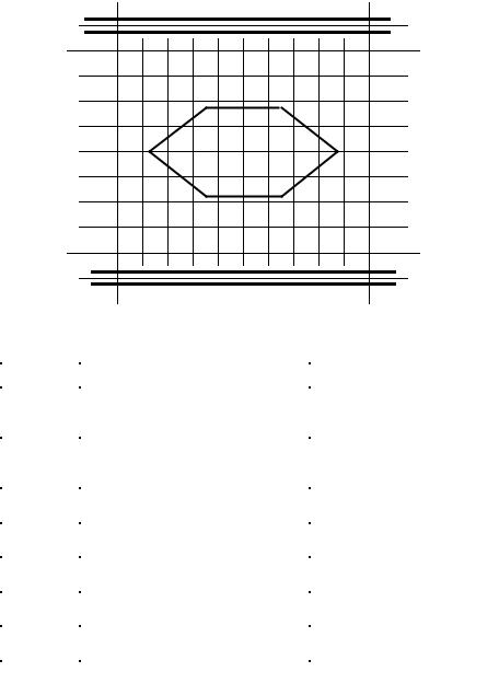
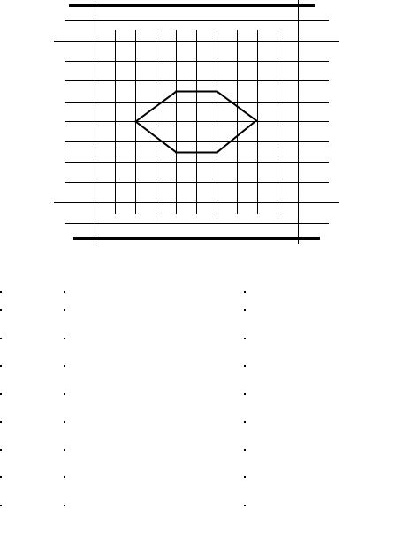
Figure 7-13 shows the transmit waveform requirements for a hub measured at TP2, and for a device (without a captive cable) measured at TP3.
Level 1 |
|
|
|
|
|
+ 400mV |
|
Point 3 |
Point 4 |
Differential |
|
|
|||
Point 1 |
Point 2 |
0 Volts |
|
Differential |
|||
|
|
||
Point 5 |
Point 6 |
- 400mV |
|
|
|
||
|
|
Differential |
|
Level 2 |
|
|
|
0% |
Unit Interval |
100% |
|
|
|
Voltage Level (D+ - D-) |
Time (% of Unit Interval) |
|
|
|
Level 1 |
525 mV in UI following a transition, |
N/A |
|
475 mV in all others |
|
|
|
|
Level 2 |
-525 mV in UI following a transition, |
N/A |
|
-475 in all others |
|
|
|
|
Point 1 |
0 V |
7.5% UI |
|
|
|
Point 2 |
0 V |
92.5% UI |
|
|
|
Point 3 |
300 mV |
37.5% UI |
|
|
|
Point 4 |
300 mV |
62.5% UI |
|
|
|
Point 5 |
-300 mV |
37.5% UI |
|
|
|
Point 6 |
-300 mV |
62.5% UI |
|
|
|
Figure 7-13. Template 1
133
Universal Serial Bus Specification Revision 2.0
Template 2
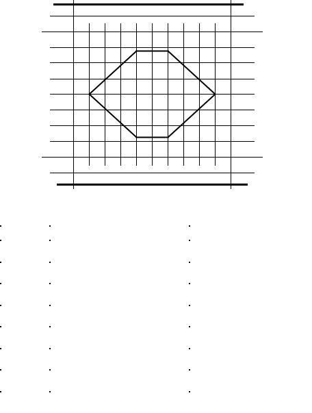
Figure 7-14 shows transmit waveform requirements for a device (with a captive cable) measured at TP2.
Level 1 |
|
|
+ 400mV |
|
Differential |
Point 3 |
Point 4 |
Point 1 |
0 Volts |
Point 2 |
|
|
Differential |
Point 5 |
Point 6 |
|
- 400mV |
|
Differential |
Level 2 |
|
Unit Interval |
|
0% |
100% |
|
Voltage Level (D+ - D-) |
Time (% of Unit Interval) |
|
|
|
Level 1 |
525 mV in UI following a transition, |
N/A |
|
475 mV in all others |
|
|
|
|
Level 2 |
-525 mV in UI following a transition, |
N/A |
|
-475 in all others |
|
|
|
|
Point 1 |
0 V |
12.5% UI |
|
|
|
Point 2 |
0 V |
87.5% UI |
|
|
|
Point 3 |
175 mV |
35% UI |
|
|
|
Point 4 |
175 mV |
65% UI |
|
|
|
Point 5 |
-175 mV |
35% UI |
|
|
|
Point 6 |
-175 mV |
65% UI |
|
|
|
Figure 7-14. Template 2
134
Universal Serial Bus Specification Revision 2.0
Template 3
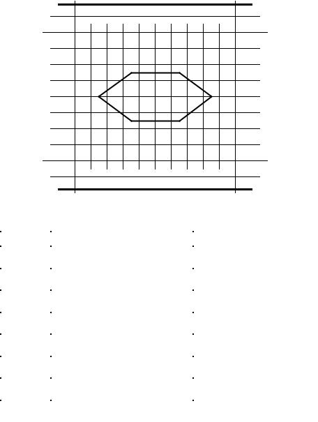
Figure 7-15 shows receiver sensitivity requirements for a device (with a captive cable) when a signal is applied at TP2.
Level 1 |
|
|
|
|
|
+ 400mV |
|
|
|
Differential |
|
Point 3 |
Point 4 |
|
|
Point 1 |
Point 2 |
0 Volts |
|
Differential |
|||
|
|
||
Poiint 5 |
Point 6 |
|
|
|
|
- 400mV |
|
|
|
Differential |
|
Level 2 |
|
|
|
0% |
Unit Interval |
100% |
|
|
|
Voltage Level (D+ - D-) |
Time (% of Unit Interval) |
|
|
|
Level 1 |
575 mV |
N/A |
|
|
|
Level 2 |
-575 mV |
N/A |
|
|
|
Point 1 |
0 V |
10% UI |
|
|
|
Point 2 |
0 V |
90% UI |
|
|
|
Point 3 |
275 mV |
40% UI |
|
|
|
Point 4 |
275 mV |
60% UI |
|
|
|
Point 5 |
-275 mV |
40% UI |
|
|
|
Point 6 |
-275 mV |
60% UI |
|
|
|
Figure 7-15. Template 3
Note: This eye is intended to specify differential data receiver sensitivity requirements. Levels 1 and 2 are outside the Disconnect Threshold values, but disconnection is detected at the source (after a minimum of 32 bit times without any transitions), not at the target receiver.
135
Universal Serial Bus Specification Revision 2.0
Template 4
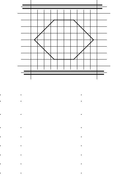
Figure 7-16 shows receiver sensitivity requirements for a device (without a captive cable) when signal is applied at TP3, and for a hub when a signal is applied at TP2.
Level 1 |
|
|
|
|
|
|
+ 400mV |
|
|
|
Differential |
|
Point 3 |
Point 4 |
|
|
Point 1 |
Point 2 |
0 Volts |
|
Differential |
||
|
|
|
|
|
Point 5 |
Point 6 |
|
|
|
|
- 400mV |
|
|
|
Differential |
Level 2 |
|
|
|
0% |
Unit Interval |
100% |
|
|
Voltage Level (D+ - D-) |
Time (% of Unit Interval) |
|
|
|
Level 1 |
575 mV |
N/A |
|
|
|
Level 2 |
-575 mV |
N/A |
|
|
|
Point 1 |
0 V |
15% UI |
|
|
|
Point 2 |
0 V |
85% UI |
|
|
|
Point 3 |
150 mV |
35% UI |
|
|
|
Point 4 |
150 mV |
65% UI |
|
|
|
Point 5 |
-150 mV |
35% UI |
|
|
|
Point 6 |
-150 mV |
65% UI |
|
|
|
Figure 7-16. Template 4
Note: This eye is intended to specify differential data receiver sensitivity requirements. Levels 1 and 2 are outside the Disconnect Threshold values, but disconnection is detected at the source (after a minimum of 32 bit times without any transitions), not at the target receiver.
136
Universal Serial Bus Specification Revision 2.0
Template 5
Figure 7-17 shows transmit waveform requirements for a hub transceiver measured at TP1 and for a device transceiver measured at TP4.
Level 1 |
|
+ 400mV |
|
|
|
||
Point 3 |
Point 4 |
Differential |
|
|
|||
Point 1 |
Point 2 |
0 Volts |
|
Differential |
|||
|
|
||
Point 5 |
Point 6 |
- 400mV |
|
|
|
||
Level 2 |
|
Differential |
|
|
|
||
0% |
Unit Interval |
100% |
|
|
|
Voltage Level (D+ - D-) |
Time (% of Unit Interval) |
|
|
|
Level 1 |
525 mV in UI following a transition, |
N/A |
|
475 mV in all others |
|
|
|
|
Level 2 |
-525 mV in UI following a transition, |
N/A |
|
-475 in all others |
|
|
|
|
Point 1 |
0 V |
5% UI |
|
|
|
Point 2 |
0 V |
95% UI |
|
|
|
Point 3 |
300 mV |
35% UI |
|
|
|
Point 4 |
300 mV |
65% UI |
|
|
|
Point 5 |
-300 mV |
35% UI |
|
|
|
Point 6 |
-300 mV |
65% UI |
|
|
|
Figure 7-17. Template 5
137
Universal Serial Bus Specification Revision 2.0
Template 6
Figure 7-18 shows receiver sensitivity requirements for a device transceiver when a signal is applied at TP4 and for a hub transceiver when a signal is applied at TP1.
Level 1 |
|
|
+ 400mV |
|
|
|
|
|
|
|
Differential |
|
Point 3 |
Point 4 |
|
|
Point 1 |
Point 2 |
0 Volts |
|
Differential |
||
|
|
|
|
|
Point 5 |
Point 6 |
|
|
|
|
- 400mV |
Level 2 |
|
|
Differential |
|
|
|
|
0% |
Unit Interval |
100% |
|
|
Voltage Level (D+ - D-) |
Time (% of Unit Interval) |
|
|
|
Level 1 |
575 mV |
N/A |
|
|
|
Level 2 |
-575 mV |
N/A |
|
|
|
Point 1 |
0 V |
20% UI |
|
|
|
Point 2 |
0 V |
80% UI |
|
|
|
Point 3 |
150 mV |
40% UI |
|
|
|
Point 4 |
150 mV |
60% UI |
|
|
|
Point 5 |
-150 mV |
40% UI |
|
|
|
Point 6 |
-150 mV |
60% UI |
|
|
|
Figure 7-18. Template 6
Note: This eye is intended to specify differential data receiver sensitivity requirements. Levels 1 and 2 are outside the Disconnect Threshold values, but disconnection is detected at the source (after a minimum of 32 bit times without any transitions), not at the target receiver.
138
Universal Serial Bus Specification Revision 2.0
High-speed Signaling Rise and Fall Times
The transition time of a high-speed driver must not be less than the specified minimum allowable differential rise and fall time (THSR and THSF). Transition times are measured when driving a reference load of 45 Ω to ground on D+ and D-. Figure 7-12 shows a recommended “Transmitter Test Fixture” for performing these measurements.
For a hub, or for a device with detachable cable, the 10% to 90% high-speed differential rise and fall times must be 500 ps or longer when measured at the A or B receptacles (respectively).
For a device with a captive cable assembly, it is a recommended design guideline that the 10% to 90% highspeed differential rise and fall times must be 500 ps or longer when measured at the point where the cable is attached to the device circuit board.
It is required that high-speed data transitions be monotonic over the minimum vertical openings specified in the preceding eye pattern templates.
7.1.2.3 Driver Usage
The upstream facing ports of functions must use one and only one of the following three driver configurations:
1.Low-speed – Low-speed drivers only
2.Full-speed – Full-speed drivers only
3.Full-/high-speed – Combination full-speed and high-speed drivers
Upstream facing USB 2.0 hub ports must use full-/high-speed drivers. Such ports must be capable of transmitting data at low-speed and full-speed rates with full-speed signaling, and at the high-speed rate using high-speed signaling. Downstream facing ports (including the host) must support low-speed, full-speed, and high-speed signaling, and must be able to transmit data at each of the three associated data rates.
In this section, there is reference to a situation in which high-speed operation is “disallowed.” This topic is discussed in depth in Chapter 11 of this specification. In brief, a high-speed capable hub's downstream facing ports are “high-speed disallowed” if the hub is unable to establish a high-speed connection on its upstream facing port. For example, this would be the case for the downstream facing ports of a high-speed capable hub when the hub is connected to a USB 1.1 host controller.
When a full-/high-speed device is attached to a pre-USB 2.0 hub, or to a hub port which is high-speed disallowed, it is required to behave as a full-speed only device. When a full-/high-speed device is attached to a USB 2.0 hub which is not high-speed disallowed, it must operate with high-speed signaling and data rate.
7.1.3 Cable Skew
The maximum skew introduced by the cable between the differential signaling pair (i.e., D+ and D- (TSKEW)) must be less than 100 ps and is measured as described in Section 6.7.
7.1.4 Receiver Characteristics
This section discusses the receiver characteristics for low-speed, full-speed, and full-/high-speed transceivers.
7.1.4.1 Low-speed and Full-speed Receiver Characteristics
A differential input receiver must be used to accept the USB data signal. The receiver must feature an input sensitivity (VDI) of at least 200 mV when both differential data inputs are in the differential common mode range (VCM) of 0.8 V to 2.5 V, as shown in Figure 7-19.
139
Universal Serial Bus Specification Revision 2.0
In addition to the differential receiver, there must be a single-ended receiver for each of the two data lines. The receivers must have a switching threshold between 0.8 V (VIL) and 2.0 V (VIH). It is recommended that the single-ended receivers incorporate hysteresis to reduce their sensitivity to noise.
Both D+ and D- may temporarily be less than VIH (min) during differential signal transitions. This period can be up to 14 ns (TFST) for full-speed transitions and up to 210 ns (TLST) for low-speed transitions. Logic in the receiver must ensure that that this is not interpreted as an SE0.
Differential Input Voltage Range
Differential Output
Crossover
Voltage Range
-1.0 |
0.0 |
0.2 |
0.4 |
0.6 |
0.8 |
1.0 |
1.2 |
1.4 |
1.6 |
1.8 |
2.0 |
2.2 |
2.4 |
2.6 |
2.8 |
3.0 |
3.2 |
4.6 |
Input Voltage Range (volts)
Figure 7-19. Differential Input Sensitivity Range for Low-/full-speed
7.1.4.2 High-speed Receiver Characteristics
A high-speed capable transceiver receiver must conform to the receiver characteristics specifications called out in Section 7.1.4.1 when receiving in low-speed or full-speed modes.
As shown in Figure 7-1, a high-speed capable transceiver which is operating in high-speed mode “listens” for an incoming serial data stream with the high-speed differential data receiver and the transmission envelope detector. Additionally, a downstream facing high-speed capable transceiver monitors the amplitude of the differential voltage on the lines with the disconnection envelope detector.
When receiving in high-speed mode, the differential receiver must be able to reliably receive signals that conform to the Receiver Eye Pattern templates shown in Section 7.1.2. Additionally, it is a strongly recommended guideline that a high-speed receiver should be able to reliably receive such signals in the presence of a common mode voltage component (VHSCM) over the range of –50 mV to 500 mV (the nominal common mode component of high-speed signaling is 200 mV). Low frequency chirp J and K signaling, which occurs during the Reset handshake, should be reliably received with a common mode voltage range of –50 mV to
600 mV.
Reception of data is qualified by the output of the transmission envelope detector. The receiver must disable data recovery when the signal falls below the high-speed squelch level (VHSSQ) defined in Table 7-3. (Detector must indicate squelch when the magnitude of the differential voltage envelope is ≤ 100 mV, and must not indicate squelch if the amplitude of differential voltage envelope is ≥ 150 mV.) Squelch detection must be done with a differential envelope detector, such as the one shown in Figure 7-1. The envelope detector used to detect the squelch state must incorporate a filtering mechanism that prevents indication of squelch during differential data crossovers.
The definition of a high-speed packet’s SYNC pattern, together with the requirements for high-speed hub repeaters, guarantee that a receiver will see at least 12 bits of SYNC (KJKJKJKJKJKK) followed by the data portion of the packet. This means that the combination of squelch response time, DLL lock time, and end of SYNC detection must occur within 12 bit times. This is required to assure that the first bit of the packet payload will be received correctly.
In the case of a downstream facing port, a high-speed capable transceiver must include a differential envelope detector that indicates when the signal on the data exceeds the high-speed Disconnect level (VHSDSC) as defined in Table 7-3. (The detector must not indicate that the disconnection threshold has been exceeded if the differential signal amplitude is ≤ 525 mV, and must indicate that the threshold has been exceeded if the differential signal amplitude is ≥ 625 mV.)
140
Universal Serial Bus Specification Revision 2.0
When sampled at the appropriate time, this detector provides indication that the device has been disconnected. The details of how the disconnection envelope detector is used are described in Section 7.1.7.3.
7.1.5 Device Speed Identification
The following sections specify the speed identification mechanisms for low-speed, full-speed, and high-speed.
7.1.5.1 Low-/Full-speed Device Speed Identification
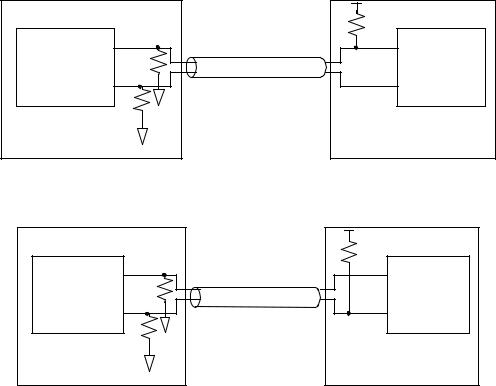
The USB is terminated at the hub and function ends as shown in Figure 7-20 and Figure 7-21. Full-speed and low-speed devices are differentiated by the position of the pull-up resistor on the downstream end of the cable:
•Full-speed devices are terminated as shown in Figure 7-20 with the pull-up resistor on the D+ line.
•Low-speed devices are terminated as shown in Figure 7-21 with the pull-up resistor on the D- line.
• |
The pull-down terminators on downstream facing ports are resistors of 15 kΩ ± 5% connected to ground. |
The design of the pull-up resistor must ensure that the signal levels satisfy the requirements specified in
Table 7-2. In order to facilitate bus state evaluation that may be performed at the end of a reset, the design must be able to pull-up D+ or D- from 0 V to VIH (min) within the minimum reset relaxation time of 2.5 µ s. A device that has a detachable cable must use a 1.5 kΩ ± 5% resistor tied to a voltage source between 3.0 V and 3.6 V (VTERM) to satisfy these requirements. Devices with captive cables may use alternative termination means. However, the Thevenin resistance of any termination must be no less than 900 Ω .
Note: Thevenin resistance of termination does not include the 15 kΩ ± 5% resistor on host/hub.
The voltage source on the pull-up resistor must be derived from or controlled by the power supplied on the USB cable such that when VBUS is removed, the pull-up resistor does not supply current on the data line to which it is attached.
|
D+ |
Full-speed or |
Rpd |
Low-speed USB |
|
Transceiver |
D- |
|
Rpd |
Host or |
|
Hub Port |
|
Z 0=90Ω ± 15%
Rpd=15KΩ ± 5%
Rpu=1.5KΩ ± 5%
Rpu |
D+ |
Full-speed USB |
Transceiver |
D- |
Hub Upstream Port |
or |
Full-speed Function |
Figure 7-20. Full-speed Device Cable and Resistor Connections
Full-speed or |
D+ |
|
|
Low-speed USB |
Rpd |
Transceiver |
D- |
|
|
|
Rpd |
Host or |
|
Hub Port |
|
Rpd=15KΩ ± 5%
Rpu=1.5KΩ ± 5%
Rpu |
|
D+ Low-speed USB |
|
|
Transceiver |
D- |
Slow Slew Rate |
|
Buffers |
Low-speed Function |
|
Figure 7-21. Low-speed Device Cable and Resistor Connections
141
Universal Serial Bus Specification Revision 2.0
7.1.5.2 High-speed Device Speed Identification
The high-speed Reset and Detection mechanisms follow the behavioral model for low-/full-speed. When reset is complete, the link must be operating in its appropriate signaling mode (low-speed, full-speed, or high-speed as governed by the preceding usage rules), and the speed indication bits in the port status register will correctly report this mode. Software need only initiate the assertion of reset and read the port status register upon notification of reset completion.
High-speed capable devices initially attach as full-speed devices. This means that for high-speed capable upstream facing ports, RPU (1.5 kΩ ± 5%) must be connected from D+ to the 3.3 V supply (as shown in Figure 7-1) through a switch which can be opened under SW control.
After the initial attachment, high-speed capable transceivers engage in a low level protocol during reset to establish a high-speed link and to indicate high-speed operation in the appropriate port status register. This protocol is described in Section 7.1.7.5.
7.1.6 Input Characteristics
The following sections describe the input characteristics for transceivers operating in low-speed, full-speed, and high-speed modes.
7.1.6.1 Low-speed and Full-speed Input Characteristics
The input impedance of D+ or D- without termination should be > 300 kΩ (ZINP). The input capacitance of a port is measured at the connector pins. Upstream facing and downstream facing ports are allowed different values of capacitance. The maximum capacitance (differential or single-ended) (CIND) allowed on a downstream facing port of a hub or host is 150 pF on D+ or D- when operating in low-speed or full-speed. This is comprised of up to 75 pF of lumped capacitance to ground on each line at the transceiver and in the connector, and an additional 75 pF capacitance on each conductor in the transmission line between the receptacle and the transceiver. The transmission line between the receptacle and RS must be 90 Ω ± 15%.
The maximum capacitance on an upstream facing port of a full-speed device with a detachable cable (CINUB) is 100 pF on D+ or D-. This is comprised of up to 75 pF of lumped capacitance to ground on each line at the transceiver and in the connector and an additional 25 pF capacitance on each conductor in the transmission line between the receptacle and the transceiver. The difference in capacitance between D+ and D- must be less than 10%.
For full-speed devices with captive cables, the device itself may have up to 75 pF of lumped capacitance to ground on D+ and D-. The cable accounts for the remainder of the input capacitance.
A low-speed device is required to have a captive cable. The input capacitance of the low-speed device will include the cable. The maximum single-ended or differential input capacitance of a low-speed device is 450 pF
(CLINUA).
For devices with captive cables, the single-ended input capacitance must be consistent with the termination scheme used. The termination must be able to charge the D+ or D- line from 0 V to VIH (min) within 2.5 µ s. The capacitance on D+/D- includes the single-ended input-capacitance of the device (measured from the pins on the connector on the cable) and the 150 pF of input capacitance of the host/hub.
An implementation may use small capacitors at the transceiver for purposes of edge rate control. The sum of the capacitance of the added capacitor (CEDGE), the transceiver, and the trace connecting capacitor and transceiver to RS must not exceed 75 pF (either single-ended or differential) and the capacitance must be balanced to within 10%. The added capacitor, if present, must be placed between the transceiver pins and RS (see Figure 7-22).
Use of ferrite beads on the D+ or D- lines of full-speed devices is discouraged.
142