

usb_2.0_english
.pdfUniversal Serial Bus Specification Revision 2.0
additional delay difference over a normal J-to-K transition is ± 5.0 ns. This limits the maximum distortion of the first bit in the packet.
Note: Because of this distortion of the SOP transition relative to the next K-to-J state transition, the first SYNC field bit should not be used to synchronize the receiver to the data stream.
The EOP must be propagated through a hub in the same way as the differential signaling. The propagation delay for sensing an SE0 must be no less than the greater of the J-to-K or K-to-J differential data delay (to avoid truncating the last data bit in a packet), but not more than 15 ns greater than the larger of these differential delays at full-speed and 200 ns at low-speed (to prevent creating a bit stuff error at the end of the packet). EOP delays are shown in Figure 7-53.
Because the sense levels for the SE0 state are not at the midpoint of the signal swing, the width of SE0 state will be changed as it passes through each hub. A hub may not change the width of the SE0 state in a full-speed EOP by more than ± 15 ns (TFHESK), as measured by the difference of the leading edge and trailing edge delays of the SE0 state (see Figure 7-53). An SE0 from a low-speed device has long rise and fall times and is subject to greater skew, but these conditions exist only on the cable from the low-speed device to the port to which it is connected. Thereafter, the signaling uses full-speed buffers and their faster rise and fall times. The SE0 from the low-speed device cannot be changed by more than ± 300 ns (TLHESK) as it passes through the hub to which the device is connected. This time allows for some signal conditioning in the low-speed transceiver to reduce its sensitivity to noise.
7.1.14.2 High-speed Hub Signaling Timings
When a hub acts as a repeater for high-speed data, the delay of the hub (THSHDD) must not exceed 36 high-speed bit times plus 4 ns (the trace delays allowed for the hub circuit board). This delay is measured from the last bit of the SYNC field at the input connector to the last bit of the SYNC field at the output connector.
A high-speed hub repeater must digitally resynchronize the buffered data, so there is no allowance for cumulative jitter (within a single packet) as a high-speed packet passes through multiple repeater stages. Within a single packet, the jitter must not exceed the eye pattern templates defined in Section 7.1.2 over a sliding window of 480 high-speed bit times.
Due to the data synchronization process, the propagation delay of a hub repeater is allowed to vary at most
5 high-speed bit times (THSHDV). The delay including this allowed variation must not exceed 36 high-speed bit times plus 4 ns. (This allows for some uncertainty as to when an incoming packet arrives at the hub with respect to the phase of the synchronization clock.)
163
Universal Serial Bus Specification Revision 2.0
7.1.15 Receiver Data Jitter
This section describes low-speed, full-speed, and high-speed receiver data jitter.
7.1.15.1 Low-/full-speed Receiver Data Jitter
The data receivers for all types of devices must be able to properly decode the differential data in the presence of jitter. The more of the bit cell that any data edge can occupy and still be decoded, the more reliable the data transfer will be. Data receivers are required to decode differential data transitions that occur in a window plus and minus a nominal quarter bit cell from the nominal (centered) data edge position. (A simple 4X oversampling state machine DPLL can be built that satisfies these requirements.) This requirement is derived in Table 7-4 and Table 7-5. The tables assume a worst-case topology of five hubs between the host and device and the worst-case number of seven bits between transitions. The derived numbers are rounded up for ease of specification.
Jitter will be caused by the delay mismatches discussed above and by mismatches in the source and destination data rates (frequencies). The receive data jitter budgets for fulland low-speed are given in Table 7-4 and Table 7-5. These tables give the value and totals for each source of jitter for both consecutive (next) and paired transitions. Note that the jitter component related to the source or destination frequency tolerance has been allocated to the appropriate device (i.e., the source jitter includes bit shifts due to source frequency inaccuracy over the worst-case data transition interval). The output driver jitter can be traded off against the device clock accuracy in a particular implementation as long as the jitter specification is met.
The low-speed jitter budget table has an additional line in it because the jitter introduced by the hub to which the low-speed device is attached is different from all the other devices in the data path. The remaining devices operate with full-speed signaling conventions (though at low-speed data rate).
Table 7-4. Full-speed Jitter Budget
Jitter Source |
|
|
|
Full-speed |
|
|
||
|
|
Next Transition |
|
Paired Transition |
||||
|
|
Each (ns) |
|
Total (ns) |
|
Each (ns) |
|
Total (ns) |
Source Driver Jitter |
2.0 |
2.0 |
1.0 |
1.0 |
||||
Source Frequency Tolerance (worst-case) |
|
0.21/bit |
|
|
0.21/bit |
|
||
|
1.5 |
|
3.0 |
|||||
Source Jitter Total |
|
|
3.5 |
|
|
4.0 |
||
Hub Jitter |
|
|
|
|
||||
3.0 |
15.0 |
1.0 |
5.0 |
|||||
Jitter Specification |
|
|
18.5 |
|
|
9.0 |
||
Destination Frequency Tolerance |
|
0.21/bit |
|
|
0.21/bit |
|
||
|
1.5 |
|
3.0 |
|||||
Receiver Jitter Budget |
|
|
|
20.0 |
|
|
|
12.0 |
164
Universal Serial Bus Specification Revision 2.0
Table 7-5. Low-speed Jitter Budget
Jitter Source |
|
Low-speed Upstream |
||
|
Next Transition |
Paired Transition |
||
|
Each (ns) |
Total (ns) |
Each (ns) |
Total (ns) |
Function Driver Jitter
Function Frequency Tolerance (worst-case)
Source (Function) Jitter Total
Hub with Low-speed Device Jitter Remaining (full-speed) Hubs’ Jitter
Jitter Specification
Host Frequency Tolerance
Host Receiver Jitter Budget
25.0 |
25.0 |
10.0 |
10.0 |
|||
|
10.0/bit |
|
|
10.0/bit |
|
|
|
|
70.0 |
|
140.0 |
||
|
|
95.0 |
|
150.0 |
||
45.0 |
|
|
|
|
|
|
45.0 |
45.0 |
45.0 |
||||
3.0 |
|
|
|
|
|
|
|
12.0 |
1.0 |
|
4.0 |
||
|
|
152.0 |
|
199.0 |
||
|
1.7/bit |
|
|
1.7/bit |
|
|
|
|
12.0 |
|
24.0 |
||
|
|
164.0 |
|
223.0 |
||
|
|
|
|
|
|
|
Low-speed Downstream
Next Transition |
Paired Transition |
||
Each (ns) |
Total (ns) |
Each (ns) |
Total (ns) |
Host Driver Jitter |
2.0 |
2.0 |
1.0 |
1.0 |
Host Frequency Tolerance (worst-case) |
1.7/bit |
|
1.7/bit |
|
12.0 |
24.0 |
|||
Source (Host) Jitter Total |
|
14.0 |
|
25.0 |
Hub with Low-speed Device Jitter |
|
|
|
|
45.0 |
45.0 |
15.0 |
15.0 |
|
Remaining (full-speed) Hubs’ Jitter |
|
|
|
|
3.0 |
12.0 |
1.0 |
4.0 |
|
Jitter Spec |
|
71.0 |
|
44.0 |
Function Frequency Tolerance |
10.0/bit |
|
10.0/bit |
|
70.0 |
140.0 |
|||
Function Receiver Jitter Budget |
|
141.0 |
|
184.0 |
Note: This table describes the host transmitting at low-speed data rate using full-speed signaling to a low-speed device through the maximum number of hubs. When the host is directly connected to the low-speed device, it uses low-speed data rate and low-speed signaling, and the host has to meet the source jitter listed in the “Jitter Specification” row.
7.1.15.2 High-speed Receiver Data Jitter
A high-speed capable receiver must reliably recover high-speed data when the waveforms at its inputs conform to the receiver sensitivity eye pattern templates. The templates, which are called out in Section 7.1.2.2, specify the horizontal and vertical eye pattern opening over a 480 bit time sliding window over the duration of a packet. Thus, for example, a high-speed receiver within a function must reliably recover data with a peak to peak jitter of 30%, measured at its B receptacle (as described by Template 4).
Such conformance is tested using Test Mode Test_Packet, as defined in Section 7.1.20.
It is a recommended design guideline that a receiver’s BER should be <= 10-12 when the receiver sensitivity requirement is met.
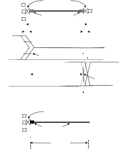
7.1.16 Cable Delay
The maximum total one-way signal propagation delay allowed is 30 ns. The allocation for cable delay is 26 ns. A maximum delay of 3 ns is allowed from a Host or Hub Controller downstream facing transceiver to its exterior downstream facing connector, while a maximum delay of 1 ns is allowed from the upstream facing connector to the upstream facing transceiver of any device. For a standard USB detachable cable, the cable
165
Universal Serial Bus Specification Revision 2.0
delay is measured from the Series A connector pins to the Series B connector pins and is no more than 26 ns. For other cables, the delay is measured from the series A connector to the point where the cable is connected to the device. The cable delay must also be less than 5.2 ns per meter.
The maximum one-way data delay on a full-speed cable is measured as shown in Figure 7-39.
One-way cable delay for low-speed cables must be less than 18 ns. It is measured as shown in Figure 7-40.
|
|
|
|
|
|
|
|
|
|
|
|
|
|
|
|
|
Traces on Board |
|
|
|
|
|
|
|
|
|
|
|
|
|
||||
|
|
|
Host/Hub |
|
|
|
|
|
|
|
|
|
|
|
|
|
|
|
|
|
|
|
|
|
|
|
|
Hub/Device |
|
|
||||
|
Downstream |
|
|
|
|
|
|
|
|
|
|
|
|
|
|
|
|
|
|
|
|
|
|
|
|
Upstream |
|
|||||||
|
|
|
|
|
|
|
|
|
|
|
|
|
|
|
|
|
|
|
|
|
|
|
|
|
|
|||||||||
|
|
|
Port |
|
|
|
|
A-Connector |
B-Connector |
|
|
|
|
|
|
|
Port |
|
||||||||||||||||
|
|
|
|
|
|
|
|
|
|
|||||||||||||||||||||||||
|
|
|
|
|
|
|
|
|
|
|
|
|
|
|
|
|
|
|||||||||||||||||
|
|
|
|
|
|
|
|
|
|
|
|
|
|
|
|
Total One-Way |
|
|
|
|
|
|
|
|
|
|
|
|
|
|
||||
|
|
|
|
|
|
|
|
|
|
|
|
|
|
|
|
|
|
|
|
|
|
|
|
|
|
|
|
|||||||
|
|
|
|
|
|
|
|
|
|
|
|
|
|
|
Propagation Delay |
|
|
|
|
|
|
|
|
|
|
|
|
|
|
|||||
|
3ns (max) |
|
|
|
|
|
|
|
|
|
|
|
|
|
30ns (max) |
|
|
|
|
|
|
|
|
|
|
1ns (max) |
||||||||
Driver End |
|
|
|
|
|
|
|
|
|
|
|
|
|
|
|
|
|
|
|
|
|
|
|
|
|
|
||||||||
of Cable |
|
|
|
|
|
|
50% Point of Initial Swing |
|
|
|
|
|
|
|
|
|
|
|
||||||||||||||||
|
|
VSS |
|
|
|
|
|
|
|
|
|
|
|
|
|
|
|
|
|
|||||||||||||||
|
|
|
|
|
|
|
|
|
|
|
|
|
|
|
|
|
|
|
|
|
|
|
|
|
|
|
|
|||||||
Receiver |
|
|
|
|
|
|
|
|
One Way Cable |
|
|
|
|
|
|
|
|
|
|
|
Data Line |
|||||||||||||
End of |
|
|
|
|
|
|
|
|
Delay 26ns |
|
|
|
|
|
|
|
|
|
|
|
Crossover |
|||||||||||||
Cable |
|
|
|
|
|
|
|
|
|
(max) |
|
|
|
|
|
|
|
|
|
|
|
Point at input of |
||||||||||||
|
|
|
|
|
|
|
|
|
|
|
|
|
|
|
||||||||||||||||||||
|
|
|
|
|
|
|
|
|
|
|
|
|
|
|
|
|
|
|
|
|
|
|
|
|
|
|
|
|
|
|
B-connector |
|||
|
|
VSS |
|
|
|
|
|
|
|
|
|
|
|
|
|
|
|
|
|
|
|
|
|
|
|
|
|
|
||||||
|
|
|
|
|
|
|
|
|
|
|
|
|
|
|
|
|
|
|
|
|
|
|
|
|
|
|
||||||||
|
|
|
|
|
|
|
|
|
|
|
|
|
|
|
|
|
|
|
|
|
|
|
|
|
|
|
|
|
|
|
|
|
|
|
|
|
|
|
|
|
|
|
|
|
|
Figure 7-39. Full-speed Cable Delay |
|||||||||||||||||||||||
|
|
|
|
|
|
|
|
|
|
|
|
|
|
|
|
|
Traces on Board |
|
|
|
|
|
|
|
|
|
|
|||||||
|
|
|
Host/Hub |
|
|
|
|
|
|
|
|
|
|
|
|
|
|
|
|
|
|
|
|
|
|
|
|
Low-speed |
|
|
||||
|
|
|
|
|
|
|
|
|
|
|
|
|
|
|
|
|
|
|
|
|
|
|
|
|
|
|||||||||
|
|
|
|
|
|
|
|
|
|
|
|
|
|
|
|
|
|
|
|
|
|
|
|
|
|
Device |
|
|
|
|||||
|
|
Downstream |
|
|
|
|
|
|
|
|
|
|
|
|
|
|
|
|
|
|
|
|
|
|
|
|
||||||||
|
|
|
|
|
|
|
|
|
|
|
|
|
|
|
|
|
|
|
|
|
|
|
||||||||||||
|
|
|
|
|
|
|
|
|
|
|
|
|
|
|
|
|
|
|
|
|
|
|
|
|
|
|
|
|
||||||
|
|
|
|
|
|
|
|
|
|
|
|
|
|
|
|
|
|
|
|
|
|
|
|
|
|
|
|
|
||||||
|
|
|
|
|
|
|
|
|
|
|
|
|
|
|
|
|
|
|
|
|
|
|
|
|
|
|
|
|
||||||
|
|
|
|
|
|
|
|
|
|
|
|
|
|
|
|
|
|
|
|
|
|
|
|
|
|
|
|
|
||||||
|
|
|
Port |
|
|
|
|
A-Connector + cable |
|
|
|
|
|
|
|
|
|
|
||||||||||||||||
|
|
|
|
|
|
|
|
|
|
|
|
|
|
|||||||||||||||||||||
|
|
|
|
|
|
|
|
|
|
|
|
|
|
|
|
|
||||||||||||||||||
|
|
|
|
|
|
|
|
|
|
|
|
|
|
|
|
|
|
|
|
|
|
|
|
|
|
|
|
|
|
|
|
|
|
|
|
|
|
|
|
|
|
|
|
|
|
|
|
|
|
|
|
|
|
|
|
|
|
|
|
|
|
|
|
|
|
|
|
|
|
|
|
|
|
|
|
|
|
|
|
|
|
|
|
|
|
|
|
|
|
|
|
|
|
|
|
|
|
|
|
|
|
|
|
|
|
|
|
|
|
|
|
|
|
|
|
|
|
|
|
|
|
|
|
|
|
|
|
|
|
|
|
|
|
|
|
|
|
|
|
|
|
|
|
|
|
|
|
|
|
|
|
|
|
|
|
|
|
|
|
|
|
|
|
|
|
|
|
|
|
|
|
|
|
|
|
|
|
|
|
|
|
|
|
|
|
|
|
|
|
|
|
|
|
|
|
|
|
|
|
|
|
|
|
|
|
|
|
|
|
|
|
|
|
|
|
|
|
|
|
|
|
|
|
|
|
|
|
|
|
|
|
|
|
|
|
|
|
|
|
|
|
|
|
|
18nS (max)
One-way Propagation Delay
Figure 7-40. Low-speed Cable Delay
166
Universal Serial Bus Specification Revision 2.0
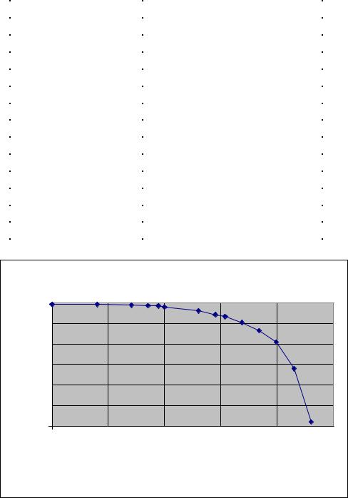
7.1.17 Cable Attenuation
USB cables must not exceed the loss figures shown in Table 7-6. Between the frequencies called out in the table, the cable loss should be no more than is shown in the accompanying graph.
Table 7-6. Maximum Allowable Cable Loss
Frequency (MHz) |
Attenuation (maximum) dB/cable |
|
|
0.064 |
0.08 |
|
|
0.256 |
0.11 |
|
|
0.512 |
0.13 |
|
|
0.772 |
0.15 |
|
|
1.000 |
0.20 |
|
|
4.000 |
0.39 |
|
|
8.000 |
0.57 |
|
|
12.000 |
0.67 |
|
|
24.000 |
0.95 |
|
|
48.000 |
1.35 |
|
|
96.000 |
1.9 |
|
|
200.00 |
3.2 |
|
|
400.00 |
5.8 |
|
|
|
Maximum Allowable Cable Loss |
|
(dB) |
0 |
|
Attenuation |
||
-1 |
||
-2 |
||
|
||
Allowable |
-3 |
|
-4 |
||
|
||
Maximum |
-5 |
|
-6 |
||
|
||
|
Frequency (log scale) from 10KHz to 1GHz, 1 decade per division |
167
Universal Serial Bus Specification Revision 2.0
7.1.18 Bus Turn-around Time and Inter-packet Delay
This section describes low-speed, full-speed, and high-speed bus turn-around time and inter-packet delay.
7.1.18.1 Low-/Full-Speed Bus Turn-around Time and Inter-packet Delay
Inter-packet delays are measured from the SE0-to-J transition at the end of the EOP to the J-to-K transition that starts the next packet.
A device must provide at least two bit times of inter-packet delay. The delay is measured at the responding device with a bit time defined in terms of the response. This provides adequate time for the device sending the EOP to drive J for one bit time and then turn off its output buffers.
The host must provide at least two bit times of J after the SE0 of an EOP and the start of a new packet (TIPD). If a function is expected to provide a response to a host transmission, the maximum inter-packet delay for a function or hub with a detachable (TRSPIPD1) cable is 6.5 bit times measured at the Series B receptacle. If the device has a captive cable, the inter-packet delay (TRSPIPD2) must be less than 7.5 bit times as measured at the Series A plug. These timings apply to both full-speed and low-speed devices and the bit times are referenced to the data rate of the packet.
The maximum inter-packet delay for a host response is 7.5 bit times measured at the host’s port pins. There is no maximum inter-packet delay between packets in unrelated transactions.
7.1.18.2 High-Speed Bus Turn-around Time and Inter-packet Delay
High-speed inter-packet delays are measured from time when the line returns to a high-speed Idle State at the end of one packet to when the line leaves the high-speed Idle State at the start of the next packet.
When transmitting after receiving a packet, hosts and devices must provide an inter-packet delay of at least 8 bit times (THSIPDOD) measured at their A or B connectors (receptacles or plugs).
Additionally, if a host is transmitting two packets in a row, the inter-packet delay must be a minimum of 88 bit times (THSIPDSD), measured at the host’s A receptacle. This will guarantee an inter-packet delay of at least 32 bit times at all devices (when receiving back to back packets). The maximum inter-packet delay provided by a host is 192 bit times within a transaction (THSRSPIPD1) measured at the A receptacle. When a host responds to a packet from a device, it will provide an inter-packet delay of at most 192 bit times measured at the A receptacle. There is no maximum inter-packet delay between packets in unrelated transactions.
When a device with a detachable cable responds to a packet from a host, it will provide an inter-packet delay of at most 192 bit times measured at the B receptacle. If the device has a captive cable, it will provide an interpacket delay of at most 192 bit times plus 52 ns (2 times the max cable length) measured at the cable's A plug
(THSRSPIPD2).
7.1.19 Maximum End-to-end Signal Delay
This section describes low-speed, full-speed, and high-speed end-to-end delay.
7.1.19.1 Low-/full-speed End-to-end Signal Delay
A device expecting a response to a transmission will invalidate the transaction if it does not see the start-of- packet (SOP) transition within the timeout period after the end of the transmission (after the SE0-to-J state transition in the EOP). This can occur between an IN token and the following data packet or between a data packet and the handshake packet (refer to Chapter 8). The device expecting the response will not time out before 16 bit times but will timeout before 18 bit times (measured at the data pins of the device from the SE0-to- J transition at the end of the EOP). The host will wait at least 18 bit times for a response to start before it will start a new transaction.
168
Universal Serial Bus Specification Revision 2.0
Figure 7-41 depicts the configuration of six signal hops (cables) that results in allowable worst-case signal delay. The maximum propagation delay from the upstream end of a hub’s cable to any downstream facing connector on that hub is 70 ns.
Host |
|
|
|
|
|
|
|
|
|
|
|
|
|
|
|
|
Hub 1 |
Hub 2 |
|
Hub 3 |
Hub 4 |
Hub 5 |
Function |
||||||||||
Controller |
|
|||||||||||||||
|
|
|
|
|
|
|
|
|
|
|
|
|
|
|
|
|
|
|
|
|
|
|
|
|
|
|
|
|
|
|
|
|
|
|
|
|
|
|
|
|
|
|
|
|
|
|
|
|
|
|
|
|
|
|
|
|
|
|
|
|
|
|
|
|
|
|
|
|
Cable Delay + Hub Delay ≤ |
70ns (each) |
|
Propagation Delay ≤ 30ns |
||||||||||||
Figure 7-41. Worst-case End-to-end Signal Delay Model for Low-/full-speed
7.1.19.2 High-Speed End-to-end Delay
A high-speed host or device expecting a response to a transmission must not timeout the transaction if the interpacket delay is less than 736 bit times, and it must timeout the transaction if no signaling is seen within 816 bit times.
These timeout limits allow a response to be seen even for the worst-case round trip signal delay. In high-speed mode, the worst-case round trip signal delay model is the sum of the following components:
12 max length cable delays (6 cables) |
= 312 ns |
|
10 max delay hubs (5 hubs) |
= |
40 ns + 360 bit times |
1 max device response time |
= |
192 bit times |
_________________________________________________________ |
||
Worst-case round trip delay |
= 352 ns +552 bit times = 721 bit times |
|
7.1.20 Test Mode Support
To facilitate compliance testing, host controllers, hubs, and high-speed capable functions must support the following test modes:
•Test mode Test_SE0_NAK: Upon command, a port’s transceiver must enter the high-speed receive mode and remain in that mode until the exit action is taken. This enables the testing of output impedance, low level output voltage, and loading characteristics. In addition, while in this mode, upstream facing ports (and only upstream facing ports) must respond to any IN token packet with a NAK handshake (only if the packet CRC is determined to be correct) within the normal allowed device response time. This enables testing of the device squelch level circuitry and, additionally, provides a general purpose stimulus/response test for basic functional testing.
•Test mode Test_J: Upon command, a port’s transceiver must enter the high-speed J state and remain in that state until the exit action is taken. This enables the testing of the high output drive level on the D+ line.
•Test mode Test_K: Upon command, a port’s transceiver must enter the high-speed K state and remain in that state until the exit action is taken. This enables the testing of the high output drive level on the D- line.
•Test mode Test_Packet: Upon command, a port must repetitively transmit the following test packet until the exit action is taken. This enables the testing of rise and fall times, eye patterns, jitter, and any other dynamic waveform specifications.
The test packet is made up by concatenating the following strings. (Note: For J/K NRZI data, and for NRZ data, the bit on the left is the first one transmitted. “S” indicates that a bit stuff occurs, which inserts an “extra” NRZI data bit. “* N” is used to indicate N occurrences of a string of bits or symbols.)
169

Universal Serial Bus Specification Revision 2.0
NRZI Symbols |
NRZ Bit Strings |
Number of NRZ Bits |
(Fields) |
|
|
|
|
|
{KJ * 15}, KK |
{00000000 * 3}, 00000001 |
32 |
(SYNC) |
|
|
|
|
|
KKJKJKKK |
11000011 |
8 |
(DATA0 PID) |
|
|
|
|
|
JKJKJKJK * 9 |
00000000 * 9 |
72 |
|
|
|
JJKKJJKK * 8 |
01010101 * 8 |
64 |
|
|
|
JJJJKKKK * 8 |
01110111 * 8 |
64 |
|
|
|
JJJJJJJKKKKKKK * 8 |
0, {111111S *15}, 111111 |
97 |
|
|
|
JJJJJJJK * 8 |
S, 111111S, {0111111S * 7} |
55 |
|
|
|
{JKKKKKKK * 10}, JK |
00111111, {S0111111 * 9}, S0 |
72 |
|
|
|
JJJKKKJJKKKKJKKK |
0110110101110011 |
16 |
(CRC16) |
|
|
|
|
|
JJJJJJJJ |
01111111 |
8 |
(EOP) |
|
|
|
|
|
A port in Test_Packet mode must send this packet repetitively. The inter-packet timing must be no less than the minimum allowable inter-packet gap as defined in Section 7.1.18 and no greater than 125 µs.
•Test mode Test_Force_Enable: Upon command, downstream facing hub ports (and only downstream facing hub ports) must be enabled in high-speed mode, even if there is no device attached. Packets arriving at the hub’s upstream facing port must be repeated on the port which is in this test mode. This enables testing of the hub’s disconnect detection; the disconnect detect bit can be polled while varying the loading on the port, allowing the disconnect detection threshold voltage to be measured.
Test Mode Entry and Exit
Test mode of a port is entered by using a device specific standard request (for an upstream facing port) or a port specific hub class request (for a downstream facing port). The device standard request SetFeature(TEST_MODE) is defined in Section 9.4.9. The hub class request SetPortFeature(PORT_TEST) is defined in Section 11.24.2.13. All high-speed capable devices/hubs must support these requests. These requests are not supported for non-high-speed devices.
The transition to test mode must be complete no later than 3 ms after the completion of the status stage of the request.
For an upstream facing port, the exit action is to power cycle the device. For a downstream facing port, the exit action is to reset the hub, as defined in Section 11.24.2.13.
170
Universal Serial Bus Specification Revision 2.0
7.2 Power Distribution
This section describes the USB power distribution specification.
7.2.1 Classes of Devices
The power source and sink requirements of different device classes can be simplified with the introduction of the concept of a unit load. A unit load is defined to be 100 mA. The number of unit loads a device can draw is an absolute maximum, not an average over time. A device may be either low-power at one unit load or highpower, consuming up to five unit loads. All devices default to low-power. The transition to high-power is under software control. It is the responsibility of software to ensure adequate power is available before allowing devices to consume high-power.
The USB supports a range of power sourcing and power consuming agents; these include the following:
•Root port hubs: Are directly attached to the USB Host Controller. Hub power is derived from the same source as the Host Controller. Systems that obtain operating power externally, either AC or DC, must supply at least five unit loads to each port. Such ports are called high-power ports. Battery-powered systems may supply either one or five unit loads. Ports that can supply only one unit load are termed lowpower ports.
•Bus-powered hubs: Draw all of their power for any internal functions and downstream facing ports from VBUS on the hub’s upstream facing port. Bus-powered hubs may only draw up to one unit load upon power-up and five unit loads after configuration. The configuration power is split between allocations to the hub, any non-removable functions and the external ports. External ports in a bus-powered hub can supply only one unit load per port regardless of the current draw on the other ports of that hub. The hub must be able to supply this port current when the hub is in the Active or Suspend state.
•Self-powered hubs: Power for the internal functions and downstream facing ports does not come from VBUS. However, the USB interface of the hub may draw up to one unit load from VBUS on its upstream facing port to allow the interface to function when the remainder of the hub is powered down. Hubs that obtain operating power externally (from the USB) must supply five unit loads to each port. Batterypowered hubs may supply either one or five unit loads per port.
•Low-power bus-powered functions: All power to these devices comes from VBUS. They may draw no more than one unit load at any time.
•High-power bus-powered functions: All power to these devices comes from VBUS. They must draw no more than one unit load upon power-up and may draw up to five unit loads after being configured.
•Self-powered functions: May draw up to one unit load from VBUS to allow the USB interface to function when the remainder of the function is powered down. All other power comes from an external (to the USB) source.
No device shall supply (source) current on VBUS at its upstream facing port at any time. From VBUS on its upstream facing port, a device may only draw (sink) current. They may not provide power to the pull-up resistor on D+/D- unless VBUS is present (see Section 7.1.5). When VBUS is removed, the device must remove power from the D+/D- pull-up resistor within 10 seconds. On power-up, a device needs to ensure that its upstream facing port is not driving the bus, so that the device is able to receive the reset signaling. Devices must also ensure that the maximum operating current drawn by a device is one unit load, until configured. Any device that draws power from the bus must be able to detect lack of activity on the bus, enter the Suspend state, and reduce its current consumption from VBUS (refer to Section 7.2.3 and Section 9.2.5.1).
171
Universal Serial Bus Specification Revision 2.0
7.2.1.1 Bus-powered Hubs
Bus-powered hub power requirements can be met with a power control circuit such as the one shown in
Figure 7-42. Bus-powered hubs often contain at least one non-removable function. Power is always available to the hub’s controller, which permits host access to power management and other configuration registers during the enumeration process. A non-removable function(s) may require that its power be switched, so that upon power-up, the entire device (hub and non-removable functions) draws no more than one unit load. Power switching on any non-removable function may be implemented either by removing its power or by shutting off the clock. Switching on the non-removable function is not required if the aggregate power drawn by it and the Hub Controller is less than one unit load. However, as long as the hub port associated with the function is in the Power-off state, the function must be logically reset and the device must appear to be not connected. The total current drawn by a bus-powered device is the sum of the current to the Hub Controller, any non-removable function(s), and the downstream facing ports.
Figure 7-42 shows the partitioning of power based upon the maximum current draw (from upstream) of five unit loads: one unit load for the Hub Controller and the non-removable function and one unit load for each of the external downstream facing ports. If more than four external ports are required, then the hub will need to be self-powered. If the non-removable function(s) and Hub Controller draw more than one unit load, then the number of external ports must be appropriately reduced. Power control to a bus-powered hub may require a regulator. If present, the regulator is always enabled to supply the Hub Controller. The regulator can also power the non-removable functions(s). Inrush current limiting must also be incorporated into the regulator subsystem.
Downstream
Upstream Hub Controller 
 Data Ports
Data Port
|
|
|
Iportctrl |
|
|
|
|
|
|
|
|
|
||
|
|
|
|
|
|
|
|
|
|
|
|
|
|
|
pstream VBUS |
|
|
Regulator |
|
On/Off |
|
|
Non-removable |
|
|
||||
|
|
|
|
|
|
|
|
|
||||||
5 unit loads |
|
|
|
|
|
|
|
Function |
|
|
||||
|
|
|
|
|
|
|
|
|
|
|
|
|||
|
|
|
|
|
|
|
|
|
|
|
|
|
||
|
|
|
|
|
|
1 unit load - Iportctrl |
|
|
|
|
|
|
||
|
|
On/Off |
|
|
|
|
|
|
|
|
|
|||
|
|
|
|
|
|
|
|
|
|
|
||||
|
|
|
Switch |
|
|
|
|
1 unit load/port |
|
|
Downstream VBUS |
|||
|
|
|
|
|
|
|
|
|
||||||
|
|
|
|
|
|
|
|
|
||||||
|
|
|
|
|
|
|
|
|
|
|
|
|
|
|
|
|
|
|
|
|
|
|
|
|
|
|
|
|
|
|
|
|
|
|
|
|
|
|
|
|
|
|
|
|
|
|
|
|
|
|
|
|
|
|
|
|
|
|
|
Figure 7-42. Compound Bus-powered Hub
Power to external downstream facing ports of a bus-powered hub must be switched. The Hub Controller supplies a software controlled on/off signal from the host, which is in the “off” state when the device is powered up or after reset signaling. When switched to the “on” state, the switch implements a soft turn-on function that prevents excessive transient current from being drawn from upstream. The voltage drop across the upstream cable, connectors, and switch in a bus-powered hub must not exceed 350 mV at maximum rated current.
7.2.1.2 Self-powered Hubs
Self-powered hubs have a local power supply that furnishes power to any non-removable functions and to all downstream facing ports, as shown in Figure 7-43. Power for the Hub Controller, however, may be supplied from the upstream VBUS (a “hybrid” powered hub) or the local power supply. The advantage of supplying the Hub Controller from the upstream supply is that communication from the host is possible even if the device’s power supply remains off. This makes it possible to differentiate between a disconnected and an unpowered device. If the hub draws power for its upstream facing port from VBUS, it may not draw more than one unit load.
172