

usb_2.0_english
.pdfUniversal Serial Bus Specification Revision 2.0
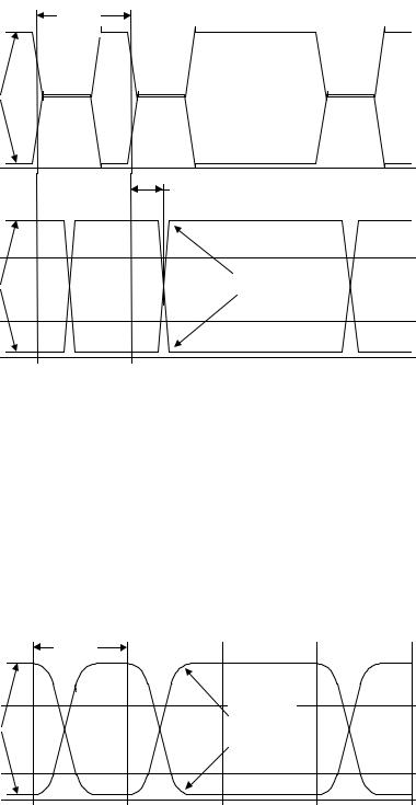
Table 7-1. Description of Functional Elements in the Example Shown in Figure 7-1 (Continued)
Transmission Envelope
Detector
Disconnection Envelope
Detector
Pull-up Resistor (RPU)
Pull-down Resistors (RPD)
This envelope detector is used to indicate that data is invalid when the amplitude of the differential signal at a receiver’s inputs falls below the squelch threshold (VHSSQ). It must indicate Squelch when the signal drops below
100 mV differential amplitude, and it must indicate that the line is not in the Squelch state when the signal exceeds 150 mV differential amplitude. The response time of the detector must be fast enough to allow a receiver to detect data transmission, to achieve DLL lock, and to detect the end of the SYNC field within 12 bit times, the minimum number of SYNC bits that a receiver is guaranteed to see. This envelope detector must incorporate a filtering mechanism that prevents indication of squelch during the longest differential data transitions allowed by the receiver eye pattern specifications.
This envelope detector is required in downstream facing ports to detect the highspeed Disconnect state on the line (VHSDSC). Disconnection must be indicated when the amplitude of the differential signal at the downstream facing driver’s connector ≥ 625 mV, and it must not be indicated when the signal amplitude is
≤ 525 mV. The output of this detector is sampled at a specific time during the transmission of the high-speed SOF EOP, as described in Section 7.1.7.3.
This resistor is required only in upstream facing transceivers and is used to indicate signaling speed capability. A high-speed capable device is required to initially attach as a full-speed device and must transition to high-speed as described in this specification. Once operating in high-speed, the 1.5 kΩ resistor must be electrically removed from the circuit. In Figure 7-1, a control line called RPU_Enable is indicated for this purpose. The preferred embodiment
is to attach matched switching devices to both the D+ and D- lines so as to keep the lines' parasitic loading balanced, even though a pull-up resistor must never be used on the D- line of an upstream facing high-speed capable transceiver.
When connected, this pull-up must meet all the specifications called out for fullspeed operation.
These resistors are required only in downstream facing transceivers and must conform to the same specifications called out for low-speed and full-speed operation.
7.1.1 USB Driver Characteristics
The USB uses a differential output driver to drive the USB data signal onto the USB cable.
For low-speed and full-speed operation, the static output swing of the driver in its low state must be below VOL (max) of 0.3 V with a 1.5 kΩ load to 3.6 V, and in its high state must be above the VOH (min) of 2.8 V with a 15 kΩ load to ground as listed in Table 7-7. Full-speed drivers have more stringent requirements, as described in Section 7.1.1.1. The output swings between the differential high and low state must be well-balanced to minimize signal skew. Slew rate control on the driver is required to minimize the radiated noise and cross talk. The driver’s outputs must support three-state operation to achieve bi-directional half-duplex operation.
Low-speed and full-speed USB drivers must never “intentionally” generate an SE1 on the bus. SE1 is a state in which both the D+ and D- lines are at a voltage above VOSE1 (min), which is 0.8 V.
High-speed drivers use substantially different signaling levels, as described in Section 7.1.1.3.
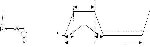
USB ports must be capable of withstanding continuous exposure to the waveforms shown in Figure 7-2 while in any drive state. These waveforms are applied directly into each USB data pin from a voltage source with an
123
Universal Serial Bus Specification Revision 2.0
output impedance of 39 Ω . The open-circuit voltage of the source shown in Figure 7-2 is based on the expected worst-case overshoot and undershoot.
AC Stress Evaluation Setup
|
|
D+ or D- pin |
|
60nS |
|
|
|
|
|
|
|||||||
on USB connector |
|
(min) |
|
|
|
|
|
|
|
||||||||
|
|
||||||||||||||||
|
nearest device |
|
|
|
|
|
|
|
|
|
|||||||
|
|
|
|
|
|
|
4.6V |
|
|||||||||
|
|
|
|
|
|
|
|
||||||||||
|
|
|
|
|
|
|
|
|
|
|
|
|
|
|
|
||
|
|
|
|
|
|
|
|
|
|
|
|
|
|
||||
|
|
|
|
RSRC |
|
4-20ns |
|||||||||||
USB |
|
|
|
|
|||||||||||||
|
|
|
|
|
|
|
|
|
|
|
|
||||||
|
|
|
|
|
|
|
|
|
|
|
|
|
|
|
|
|
|
Device |
|
|
V |
|
|
|
|
|
|
|
|
|
|
|
|||
|
|
|
|
|
|
|
|
|
|
|
|
|
|
|
|||
|
|
|
|
|
|
|
|
|
|
|
|
|
-1.0V |
||||
|
|
|
|
|
|
|
|
|
|
|
|
||||||
|
|
|
|
|
|
|
|
|
|
|
|||||||
|
|
|
|
|
|
|
|
|
|
|
|
|
|
|
|
||
|
|
|
|
|
|
|
|
|
|
|
|
|
|
166.7ns |
|||
RSRC = 39Ω ± 2% |
|
(6MHz) |
|
||
|
|
|
The signal produced by the voltage generator may be |
|
|
distorted when observed at the data pin due to input |
|
|
protection devices possibly incorporated in the USB |
|
|
device. |
|
|
Figure 7-2. Maximum Input Waveforms for USB Signaling
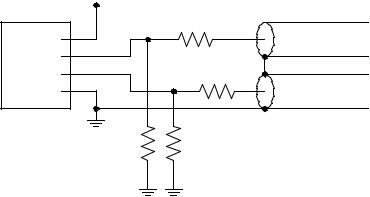
Short Circuit Withstand
A USB transceiver is required to withstand a continuous short circuit of D+ and/or D- to VBUS, GND, other data line, or the cable shield at the connector, for a minimum of 24 hours without degradation. It is recommended that transceivers be designed so as to withstand such short circuits indefinitely. The device must not be damaged under this short circuit condition when transmitting 50% of the time and receiving 50% of the time (in all supported speeds). The transmit phase consists of a symmetrical signal that toggles between drive high and drive low. This requirement must be met for max value of VBUS (5.25 V).
It is recommended that these AC and short circuit stresses be used as qualification criteria against which the long-term reliability of each device is evaluated.
7.1.1.1 Full-speed (12 Mb/s) Driver Characteristics
A full-speed USB connection is made through a shielded, twisted pair cable with a differential characteristic impedance (Z0) of 90 Ω ± 15%, a common mode impedance (ZCM) of 30 Ω ± 30%, and a maximum one-way delay (TFSCBL) of 26 ns. When the full-speed driver is not part of a high-speed capable transceiver, the impedance of each of the drivers (ZDRV) must be between 28 Ω and 44 Ω , i.e., within the gray area in Figure 7-4. When the full-speed driver is part of a high-speed capable transceiver, the impedance of each of the drivers (ZHSDRV) must be between 40.5 Ω and 49.5 Ω , i.e., within the gray area in Figure 7-5.
For a CMOS implementation, the driver impedance will typically be realized by a CMOS driver with an impedance significantly less than this resistance with a discrete series resistor making up the balance as shown in Figure 7-3. The series resistor RS is included in the buffer impedance requirement shown in Figure 7-4 and Figure 7-5. In the rest of the chapter, references to the buffer assume a buffer with the series impedance unless stated otherwise.
124
Universal Serial Bus Specification Revision 2.0
|
Buffer Output Imped. (ZBUF) |
|
TxD+ |
RS |
|
D+ (28Ω to 44Ω Equiv. Imped.) |
||
|
||
OE |
Identical |
|
CMOS |
||
|
Buffers |
TxD- |
D- (28Ω to 44Ω Equiv. Imped.) |
|
|
|
RS |
Figure 7-3. Example Full-speed CMOS Driver Circuit (non High-speed capable)
Full-speed Buffers in Transceivers Which are Not High-speed Capable
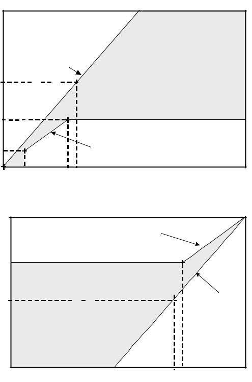
The buffer impedance must be measured for driving high as well as driving low. Figure 7-4 shows the composite V/I characteristics for the full-speed drivers with included series damping resistor (RS). The characteristics are normalized to the steady-state, unloaded output swing of the driver. The normalized driver characteristics are found by dividing the measured voltages and currents by the actual swing of the driver under test. The normalized V/I curve for the driver must fall entirely inside the shaded region. The V/I region is bounded by the minimum driver impedance above and the maximum driver impedance below. The minimum drive region is intersected by a constant current region of |6.1VOH| mA when driving low and -|6.1VOH| mA when driving high. In the special case of a full-speed driver which is driving low, and which is part of a highspeed capable transceiver, the low drive region is intersected by a constant current region of 22.0 mA. This is the minimum current drive level necessary to ensure that the waveform at the receiver crosses the opposite single-ended switching level on the first reflection.
When testing, the current into or out of the device need not exceed ± 10.71*VOH mA and the voltage applied to D+/D- need not exceed 0.3*VOH for the drive low case and need not drop below 0.7*VOH for the drive high case.
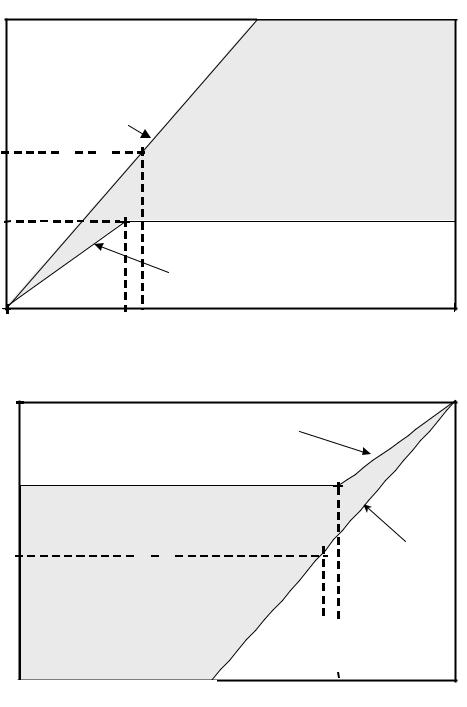
Full-speed Buffers in High-speed Capable Transceivers
Figure 7-5 shows the V/I characteristics for a Full-speed buffer which is part of a high-speed capable transceiver. The output impedance, ZHSDRV (including the contribution of RS), is required to be between 40.5  and 49.5
  . Additionally, the output voltage must be within 10mV of ground when no current is flowing in or out of the pin (VHSTERM).
125
Universal Serial Bus Specification Revision 2.0
|
|
drive low |
|
|
|
|
IOUT |
|
|
|
|
|
|
(mA) |
Slope = 1/28Ω |
|
|
|
|
|
|
|
|
|
|
||
10.71 * |VOH| |
Test Limit |
|
|
|
|
|
6.1 * |VOH| |
|
|
|
|
|
|
2.32 |
|
|
Slope = 1/44Ω |
|
||
0 |
|
|
|
|
|
|
0 |
0.3V |
0.27*VOH |
0.3*VOH |
VOUT |
(Volts) |
VOH |
|
|
|
|
|
||
0 |
|
|
|
|
|
drive high |
|
|
|
|
Slope = 1/44Ω |
|
|
|
-6.1*|VOH| |
|
|
|
|
-10.71 * |VOH| |
Test Limit |
|
Slope = 1/28Ω |
|
|
|
|
||
|
|
|
|
|
IOUT |
|
|
|
|
(mA) |
|
|
|
|
0 |
VOUT (Volts) |
0.7*VOH |
0.73*VOH |
VOH |
Figure 7-4. Full-speed Buffer V/I Characteristics
126
Universal Serial Bus Specification Revision 2.0
|
drive low |
|
|
IOUT |
|
|
|
(mA) |
Slope = 1/40.5Ω |
|
|
|
|
|
|
10.71 * |VOH| |
Test Limit |
|
|
22.0 |
|
|
|
|
Slope = 1/49.5Ω |
|
|
0 |
|
|
|
0 |
1.09V 0.434*VOH |
VOUT (Volts) |
VOH |
0 |
|
|
|
drive high
Slope = 1/49.5Ω
-6.1*|VOH|
-10.71 * |VOH| |
Test Limit |
|
Slope = 1/40.5Ω |
||
|
IOUT
(mA)
0 |
VOUT (Volts) |
|
|
|
|
VOH |
|
|
|
|
|||
|
|
|
|
|||
|
|
|
|
|||
|
|
|
|
|||
|
|
|
|
|||
|
|
|
|
|||
|
|
|
|
|||
|
|
|
|
|||
|
|
|
|
|||
|
|
|
|
|||
0.566*VOH |
0.698*VOH |
|||||
Figure 7-5. Full-speed Buffer V/I Characteristics for High-speed Capable Transceiver
127
Universal Serial Bus Specification Revision 2.0
Figure 7-6 shows the full-speed driver signal waveforms.
One Bit
Time
(12Mb/s)
Driver
Signal Pins
VSS
VIH (min)
Receiver
Signal Pins
One-Way
Trip Cable |
Delay |
Signal pins pass |
input spec levels |
after one cable |
delay |
VIL (max)
VSS
Figure 7-6. Full-speed Signal Waveforms
7.1.1.2 Low-speed (1.5 Mb/s) Driver Characteristics
A low-speed device must have a captive cable with the Series A connector on the plug end. The combination of the cable and the device must have a single-ended capacitance of no less than 200 pF and no more than 450 pF on the D+ or D- lines.
The propagation delay (TLSCBL) of a low-speed cable must be less than 18 ns. This is to ensure that the reflection occurs during the first half of the signal rise/fall, which allows the cable to be approximated by a lumped capacitance.
Figure 7-7 shows the low-speed driver signal waveforms.
VIH (min)
Driver
Signal Pins
VIL (max)
VSS
One Bit |
Time |
(1.5Mb/s) |
Signal pins |
pass output |
spec levels |
with minimal |
reflections and |
ringing |
Figure 7-7. Low-speed Driver Signal Waveforms
128
Universal Serial Bus Specification Revision 2.0
7.1.1.3 High-speed (480 Mb/s) Driver Characteristics
A high-speed USB connection is made through a shielded, twisted pair cable with a differential characteristic impedance (Z0) of 90 Ω ± 15%, a common mode impedance (ZCM) of 30 Ω ± 30%, and a maximum one-way delay of 26 ns (TFSCBL). The D+ and D- circuit board traces which run between a transceiver and its associated connector should also have a nominal differential impedance of 90 Ω , and together they may add an additional 4 ns of delay between the transceivers. (See Section 7.1.6 for details on impedance specifications of boards and transceivers.) The differential output impedance of a high-speed capable driver is required to be 90 Ω ± 10%.
When either the D+ or D- lines are driven high, VHSOH (the high-speed mode high-level output voltage driven on a data line with a precision 45 Ω load to GND) must be 400 mV ± 10%. On a line which is not driven, either because the transceiver is not transmitting or because the opposite line is being driven high, VHSOL (the highspeed mode low-level output voltage driven on a data line with a 45 Ω load to GND) must be 0 V ± 10 mV.
Note: Unless indicated otherwise, all voltage measurements are to be made with respect to the local circuit ground.
Note: This specification requires that a high-speed capable transceiver operating in full-speed or low-speed mode must have a driver impedance (ZHSDRV) of 45 Ω ± 10%. It is recommended that the driver impedances be matched to within 5 Ω within a transceiver. For upstream facing transceivers which do not support high-speed mode, the driver output impedance (ZDRV) must fall within the range of 28 Ω to 44 Ω .
On downstream facing ports, RPD resistors (15 kΩ ± 5%) must be connected from D+ and D- to ground.
When a high-speed capable transceiver transitions to high-speed mode, the high-speed idle state is achieved by driving SE0 with the low-/full-speed drivers at each end of the link (so as to provide the required terminations), and by disconnecting the D+ pull-up resistor in the upstream facing transceiver.
In the preferred embodiment, a transceiver activates its high-speed current driver only when transmitting highspeed signals. This is a potential design challenge, however, since the signal amplitude and timing specifications must be met even on the first symbol within a packet. As a less efficient alternative, a transceiver may cause its high-speed current source to be continually active while in high-speed mode. When the transceiver is not transmitting, the current may be directed into the device ground rather than through the current steering switch which is used for data signaling. In the example circuit, steering the current to ground is accomplished by setting HS_Drive_Enable low.
In CMOS implementations, the driver impedance will typically be realized by the combination of the driver’s intrinsic output impedance and RS. To optimally control ZHSDRV and to minimize parasitics, it is preferred the driver impedance be minimized (under 5 Ω ) and the balance of the 45 Ω should be contributed by the RS component.
When a transceiver operating in high-speed mode transmits, the transmit current is directed into either the D+ or D- data line. A J is asserted by directing the current to the D+ line, a K by directing it to the D- line.
When each of the data lines is terminated with a 45 Ω resistor to the device ground, the effective load resistance on each side is 22.5 Ω . Therefore, the line into which the drive current is being directed rises to 17.78 ma * 22.5 Ω or 400 mV (nominal). The other line remains at the device ground voltage. When the current is directed to the opposite line, these voltages are reversed.
7.1.2 Data Signal Rise and Fall, Eye Patterns
The following sections specify the data signal rise and fall times for full-speed and low-speed signaling, and the rise time and eye patterns for high-speed signaling.
129
Universal Serial Bus Specification Revision 2.0
7.1.2.1 Low-speed and Full-speed Data Signal Rise and Fall
For low-speed and full-speed, the output rise time and fall times are measured between 10% and 90% of the signal (Figure 7-8). Rise and fall time requirements apply to differential transitions as well as to transitions between differential and single-ended signaling.
The rise and fall times for full-speed buffers are measured with the load shown in Figure 7-9. The rise and fall times must be between 4 ns and 20 ns and matched to within ± 10% to minimize RFI emissions and signal skew. The transitions must be monotonic.
The rise and fall times for low-speed buffers are measured with the load shown in Figure 7-10. The capacitive load shown in Figure 7-10 is representative of the worst-case load allowed by the specification. A downstream facing transceiver is allowed 150 pF of input/output capacitance (CIND). A low-speed device (including cable) may have a capacitance of as little as 200 pF and as much as 450 pF. This gives a range of 200 pF to 600 pF as the capacitive load that a downstream facing low-speed buffer might encounter. Upstream facing buffers on low-speed devices must be designed to drive the capacitance of the attached cable plus an additional 150 pF. If a low-speed buffer is designed for an application where the load capacitance is known to fall in a different range, the test load can be adjusted to match the actual application. Low-speed buffers on hosts and hubs that are attached to USB receptacles must be designed for the 200 pF to 600 pF range. The rise and fall time must be between 75 ns and 300 ns for any balanced, capacitive test load. In all cases, the edges must be matched to within ± 20% to minimize RFI emissions and signal skew. The transitions must be monotonic.
For both full-speed and low-speed signaling, the crossover voltage (VCRS) must be between 1.3 V and 2.0 V.
For low-speed and full-speed, this specification does not require matching signal swing matching to any greater degree than described above. However, when signaling, it is preferred that the average voltage on the D+ and D- lines should be constant. This means that the amplitude of the signal swing on both D+ and D- should be the same; the low and high going transition should begin at the same time and change at the same rate; and the crossover voltage should be the same when switching to a J or K. Deviations from signal matching will result in common-mode noise that will radiate and affect the ability of devices and systems to pass tests that are mandated by government agencies.
|
Rise Time |
|
|
Fall Time |
|||||||||||||
VCRS |
90% |
90% |
|
|
|
|
|
|
|
|
|
|
|||||
|
|
|
|
|
|
|
|
|
|
||||||||
|
|
|
|
|
|
|
|
|
|
|
|
|
|
|
|
|
|
|
10% |
|
|
|
|
|
|
|
|
|
|
|
|
10% |
|||
Differential |
|
|
tR |
|
|
|
|
|
|
tF |
|
|
|
||||
|
|
|
|
|
|
|
|
|
|
|
|
|
|||||
Data Lines |
|
|
|
|
|
|
|
|
|
|
|
|
|
||||
|
|
||||||||||||||||
|
|
|
|
|
|||||||||||||
|
|
|
|
|
|
|
|
|
|
|
|
|
|||||
Figure 7-8. Data Signal Rise and Fall Time
Full-speed
Buffer
RS
TxD+

 CL
CL
RS
TxD-

 CL
CL
CL = 50pF
Figure 7-9. Full-speed Load
130
Universal Serial Bus Specification Revision 2.0
Low-speed |
|
Low-speed |
|
Buffer |
|
Buffer |
|
RS |
|
RS |
|
TxD+ |
|
TxD+ |
|
CL |
3.6V |
CL |
15KΩ |
RS |
1.5KΩ |
RS |
|
TxD- |
|
TxD- |
|
CL |
|
CL |
15KΩ |
|
|
||
CL = 200pF to 600pF |
|
CL = 50pF to 150pF |
|
Low-speed downstream port load |
Low-speed upstream port load |
|
|
Figure 7-10. Low-speed Port Loads
Note: The CL for low-speed port load only represents the range of loading that might be added when the lowspeed device is attached to a hub. The low-speed buffer must be designed to drive the load of its attached cable plus CL. A low-speed buffer design that can drive the downstream test load would be capable of driving any legitimate upstream load.
7.1.2.2 High-speed Signaling Eye Patterns and Rise and Fall Time
The following specifications apply to high-speed mode signaling. All bits, including the first and last bit of a packet, must meet the following eye pattern requirements for timing and amplitude.
T P 1 |
T P 2 |
T P 3 |
T P 4 |
Tra ces |
U SB C able |
Traces |
|
T ransceiver |
A |
B |
T ransceiver |
C onnector |
Conn ector |
|
|
H ub Circuit Boa rd |
Device C ircuit Board |
||
Figure 7-11. Measurement Planes
Figure 7-11 defines four test planes which will be referenced in this section. TP1 and TP4 are the points where the transceiver IC pins are soldered to the hub and device circuit boards, respectively. TP2 is at the mated pins of the A connector, and TP3 is at the mated pins of the B connector (or, in the case of a captive cable, where the cable is attached to the circuit board). The following differential eye pattern templates specify transmit waveform and receive sensitivity requirements at various points and under various conditions.
When testing high-speed transmitters and receivers, measurements are made with the Transmitter/Receiver Test Fixture shown in Figure 7-12. In either case, the fixture is attached to the USB connector closest to the transceiver being tested.
131
Universal Serial Bus Specification Revision 2.0
Transmitter Test Attenuation: Voltage at Scope Inputs = 0.760 * Voltage at Transmitter Outputs Receiver Test Attenuation: Voltage at Receiver Inputs = 0.684 * Voltage at Data Generator Outputs
|
Test Supply Voltage |
|
|
|
|
15.8 Ohms |
|
USB |
Vbus |
50 Ohm |
|
Coax |
|||
Connector |
|||
D+ |
|
||
Nearest |
|
||
D- |
15.8 Ohms |
||
Device |
|||
Gnd |
50 Ohm |
||
Under Test |
|||
|
Coax |
||
|
|
||
|
143 |
143 |
|
|
Ohms |
Ohms |
+
To 50 Ohm Inputs of a High Speed Differential Oscilloscope, or 50 Ohm Outputs of a High Speed Differential Data Generator
-
Figure 7-12. Transmitter/Receiver Test Fixture
Note: When testing the upstream facing port of a device, VBUS must be provided from the time the device is placed in the appropriate test mode until the test is completed. This requirement will likely necessitate additional switching functionality in the test fixture (for example, to switch the D+ and D- lines between the host controller and the test instrument). Such additions must have minimal impact on the high frequency measurement results.
Transmit eye patterns specify the minimum and maximum limits, as well as limits on timing jitter, within which a driver must drive signals at each of the specified test planes. Receive eye patterns specify the minimum and maximum limits, as well as limits on timing jitter, within which a receiver must recover data.
Conformance to Templates 1, 2, 3, and 4 is required for USB 2.0 hubs and devices:
Template 1: Transmit waveform requirements for hub measured at TP2, and for device (without a captive cable) measured at TP3
Template 2: Transmit waveform requirements for device (with a captive cable) measured at TP2
Template 3: Receiver sensitivity requirements for device (with a captive cable) when signal is applied at TP2
Template 4: Receiver sensitivity requirements for device (without a captive cable) when signal is applied at TP3, and for hub when signal is applied at TP2
Templates 5 and 6 are recommended guidelines for designers:
Template 5: Transmit waveform requirements for hub transceiver measured at TP1, and for device transceiver measured at TP4
Template 6: Receiver sensitivity requirements for device transceiver when signal is applied at TP4, and for hub transceiver at when signal is applied at TP1
132