

usb_2.0_english
.pdfUniversal Serial Bus Specification Revision 2.0
|
|
|
|
|
|
|
Upstream VBUS |
|
|
. |
|||
Regulator |
|
. |
||||
1 unit load (max) |
Hub Controller |
|||||
|
|
. |
||||
Upstream |
|
|
||||
|
|
|
|
|
|
|
Data Port |
|
|
|
|
|
|
|
|
|
|
|
|
|
|
|
|
|
|
|
|
Downstream
Data Ports
Local Power |
|
|
|
|
Regulator |
|
Non-removable |
|
|||
|
|
|
|
|
Function |
|
|||||
Supply |
|
|
|
|
|
|
|
|
|||
|
|
On/Off |
|
|
|
|
|
||||
|
|
|
|
|
|
|
|
|
|||
|
|
|
|
|
|
|
|
||||
|
|
|
|
|
|
|
|
||||
|
|
|
|
|
|
|
|
|
|
. |
|
|
|
|
|
|
|
|
|
|
|||
|
|
|
|
|
|
|
Current Limit |
|
. |
||
|
|
|
|
|
|
|
|
|
|
|
|
5 unit loads/port |
Downstream VBUS |
|
Current Limit |
. |
. |
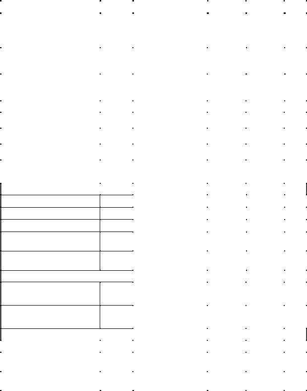
Figure 7-43. Compound Self-powered Hub
The number of ports that can be supported is limited only by the address capability of the hub and the local supply.
Self-powered hubs may experience loss of power. This may be the result of disconnecting the power cord or exhausting the battery. Under these conditions, the hub may force a re-enumeration of itself as a bus-powered hub. This requires the hub to implement port power switching on all external ports. When power is lost, the hub must ensure that upstream current does not exceed low-power. All the rules of a bus-powered hub then apply.
7.2.1.2.1 Over-current Protection
The host and all self-powered hubs must implement over-current protection for safety reasons, and the hub must have a way to detect the over-current condition and report it to the USB software. Should the aggregate current drawn by a gang of downstream facing ports exceed a preset value, the over-current protection circuit removes or reduces power from all affected downstream facing ports. The over-current condition is reported through the hub to Host Controller, as described in Section 11.12.5. The preset value cannot exceed 5.0 A and must be sufficiently above the maximum allowable port current such that transient currents (e.g., during power up or dynamic attach or reconfiguration) do not trip the over-current protector. If an over-current condition occurs on any port, subsequent operation of the USB is not guaranteed, and once the condition is removed, it may be necessary to reinitialize the bus as would be done upon power-up. The over-current limiting mechanism must be resettable without user mechanical intervention. Polymeric PTCs and solid-state switches are examples of methods, which can be used for over-current limiting.
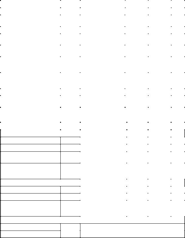
7.2.1.3 Low-power Bus-powered Functions
A low-power function is one that draws up to one unit load from the USB cable when operational. Figure 7-44 shows a typical bus-powered, low-power function, such as a mouse. Low-power regulation can be integrated into the function silicon. Low-power functions must be capable of operating with input VBUS voltages as low as 4.40 V, measured at the plug end of the cable.
173
Universal Serial Bus Specification Revision 2.0
Upstream |
|
|
Function |
|
Data Port |
||||
|
||||
|
|
|
|
|
Upstream V BUS 
 Regulator
1 unit load (max)
Figure 7-44. Low-power Bus-powered Function
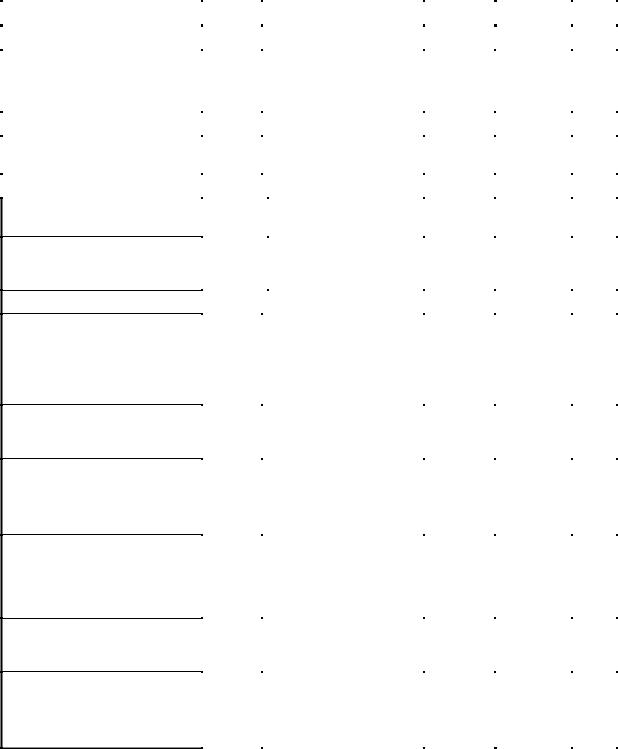
7.2.1.4 High-power Bus-powered Functions
A function is defined as being high-power if, when fully powered, it draws over one but no more than five unit loads from the USB cable. A high-power function requires staged switching of power. It must first come up in a reduced power state of less than one unit load. At bus enumeration time, its total power requirements are obtained and compared against the available power budget. If sufficient power exists, the remainder of the function may be powered on. A typical high-power function is shown in Figure 7-45. The function’s electronics have been partitioned into two sections. The function controller contains the minimum amount of circuitry necessary to permit enumeration and power budgeting. The remainder of the function resides in the function block. High-power functions must be capable of operating in their low-power (one unit load) mode with an input voltage as low as 4.40 V, so that it may be detected and enumerated even when plugged into a buspowered hub. They must also be capable of operating at full power (up to five unit loads) with a VBUS voltage of 4.75 V, measured at the upstream plug end of the cable.
Upstream |
|
|
Function Controller |
|
|
|
Function |
|||
|
|
|
||||||||
Data Port |
|
|
|
|||||||
|
|
|
|
|
|
|
||||
|
|
|
|
|
|
|
|
On/Off |
|
|
|
|
|
|
1 unit load |
|
|
||||
|
|
|
|
|
|
|
|
|
||
|
|
|
|
(max) |
|
|
|
|
|
|
Upstream VBUS |
|
|
|
|
|
|
|
|
||
|
Regulator |
|
|
|
|
|||||
5 unit loads (max) |
|
|
|
|
|
|||||
Figure 7-45. High-power Bus-powered Function
7.2.1.5 Self-powered Functions
Figure 7-46 shows a typical self-powered function. The function controller is powered either from the upstream bus via a low-power regulator or from the local power supply. The advantage of the former scheme is that it permits detection and enumeration of a self-powered function whose local power supply is turned off. The maximum upstream power that the function controller can draw is one unit load, and the regulator block must implement inrush current limiting. The amount of power that the function block may draw is limited only by the local power supply. Because the local power supply is not required to power any downstream bus ports, it does not need to implement current limiting, soft start, or power switching.
174
Universal Serial Bus Specification Revision 2.0
Upstream |
Function Controller |
|
|
|
Function |
||
|
|
|
|
|
|
||
Data Port |
|
|
|
||||
|
|
|
|
|
|||
|
|
|
|
|
|
|
|
Upstream VBUS |
Regulator |
1 unit load (max) |
Local Power |
|
Regulator |
Supply |
|
|
|
|
|
|
|
|
Figure 7-46. Self-powered Function
7.2.2 Voltage Drop Budget
The voltage drop budget is determined from the following:
•The voltage supplied by high-powered hub ports is 4.75 V to 5.25 V.
•The voltage supplied by low-powered hub ports is 4.4 V to 5.25 V.
•Bus-powered hubs can have a maximum drop of 350 mV from their cable plug (where they attach to a source of power) to their output port connectors (where they supply power).
•The maximum voltage drop (for detachable cables) between the A-series plug and B-series plug on VBUS is 125 mV (VBUSD).
•The maximum voltage drop for all cables between upstream and downstream on GND is 125 mV (VGNDD).
•All hubs and functions must be able to provide configuration information with as little as 4.40 V at the connector end of their upstream cables. Only low-power functions need to be operational with this minimum voltage.
•Functions drawing more than one unit load must operate with a 4.75 V minimum input voltage at the connector end of their upstream cables.
Figure 7-47 shows the minimum allowable voltages in a worst-case topology consisting of a bus-powered hub driving a bus-powered function.
Host or |
|
|
|
|
|
Bus-powered |
|
|
|
|
Low-power |
||||||||
Powered Hub |
|
|
|
|
|
|
Hub |
|
|
|
|
|
|
|
Function |
||||
|
|
|
|
4.735V |
4.640V |
|
|
|
|
|
|
|
4.397V |
4.378V |
|
|
|
|
|
|
4.750V |
|
|
|
4.625V |
|
|
*4.400V |
|
|
|
|
4.375V |
|
|||||
|
|
|
|
|
|
|
|
4.500V |
|
|
|
|
|
|
|
|
|
||
|
|
|
|
|
|
|
|
|
|
|
|
|
|
|
4.350V |
||||
|
|
|
|
|
|
|
|
|
|
|
|
|
|
|
|||||
|
|
|
|
|
|
|
|
|
|
|
|
|
|
|
|||||
|
|
|
|
|
|
|
|
|
|
|
|
|
|
|
|
|
|
|
|
0.000V |
0.015V |
0.110V |
0.125V |
0.000V |
0.003V |
0.022V |
0.025V |
|
|
|
|
Referenced |
Referenced |
to Source |
to Hub |
*Under transient conditions, supply at hub can drop from 4.400V to 4.070V
Figure 7-47. Worst-case Voltage Drop Topology (Steady State)
175
Universal Serial Bus Specification Revision 2.0
7.2.3 Power Control During Suspend/Resume
Suspend current is a function of unit load allocation. All USB devices initially default to low-power. Lowpower devices or high-power devices operating at low-power are limited to 500 A of suspend current. If the device is configured for high-power and enabled as a remote wakeup source, it may draw up to 2.5 mA during suspend. When computing suspend current, the current from VBUS through the bus pull-up and pull-down resistors must be included. Configured bus-powered hubs may also consume a maximum of 2.5 mA, with
500 A allocated to each available external port and the remainder available to the hub and its internal functions. If a hub is not configured, it is operating as a low-power device and must limit its suspend current to 500 A.
While in the Suspend state, a device may briefly draw more than the average current. The amplitude of the current spike cannot exceed the device power allocation 100 mA (or 500 mA). A maximum of 1.0 second is allowed for an averaging interval. The average current cannot exceed the average suspend current limit (ICCSH or ICCSL, see Table 7-7) during any 1.0-second interval (TSUSAVG1). The profile of the current spike is restricted so the transient response of the power supply (which may be an efficient, low-capacity, trickle power supply) is not overwhelmed. The rising edge of the current spike must be no more than 100 mA/ s. Downstream facing ports must be able to absorb the 500 mA peak current spike and meet the voltage droop requirements defined for inrush current during dynamic attach (see Section 7.2.4.1). Figure 7-48 illustrates a typical example profile for an averaging interval. If the supply to the pull-up resistor on D+/D- is derived from VBUS, then the suspend current will never go to zero because the pull-up and pull-down resistors will always draw power.
ICONFIGURED(max)
Edge rate must |
Current Spike |
|
|
||
not exceed |
|
|
100mA/ s |
|
|
|
|
ICCS(H|L) |
I |
|
|
|
0 mA |
|
|
|
|
|
|
|
Averaging Interval
time
Figure 7-48. Typical Suspend Current Averaging Profile
Devices are responsible for handling the bus voltage reduction due to the inductive and resistive effects of the cable. When a hub is in the Suspend state, it must still be able to provide the maximum current per port (one unit load of current per port for bus-powered hubs and five unit loads per port for self-powered hubs). This is necessary to support remote wakeup-capable devices that will power-up while the remainder of the system is still suspended. Such devices, when enabled to do remote wakeup, must drive resume signaling upstream within 10 ms of starting to draw the higher, non-suspend current. Devices not capable of remote wakeup must draw the higher current only when not suspended.
When devices wakeup, either by themselves (remote wakeup) or by seeing resume signaling, they must limit the inrush current on VBUS. The target maximum droop in the hub VBUS is 330 mV. The device must have sufficient on-board bypass capacitance or a controlled power-on sequence such that the current drawn from the hub does not exceed the maximum current capability of the port at any time while the device is waking up.
176
Universal Serial Bus Specification Revision 2.0
7.2.4 Dynamic Attach and Detach
The act of plugging or unplugging a hub or function must not affect the functionality of another device on other segments of the network. Unplugging a function will stop the transaction between that function and the host. However, the hub to which this function was attached will recover from this condition and will alert the host that the port has been disconnected.
7.2.4.1 Inrush Current Limiting
When a function or hub is plugged into the network, it has a certain amount of on-board capacitance between VBUS and ground. In addition, the regulator on the device may supply current to its output bypass capacitance and to the function as soon as power is applied. Consequently, if no measures are taken to prevent it, there could be a surge of current into the device which might pull the VBUS on the hub below its minimum operating level. Inrush currents can also occur when a high-power function is switched into its high-power mode. This problem must be solved by limiting the inrush current and by providing sufficient capacitance in each hub to prevent the power supplied to the other ports from going out of tolerance. An additional motivation for limiting inrush current is to minimize contact arcing, thereby prolonging connector contact life.
The maximum droop in the hub VBUS is 330 mV, or about 10% of the nominal signal swing from the function. In order to meet this requirement, the following conditions must be met:
•The maximum load (CRPB) that can be placed at the downstream end of a cable is 10 µ F in parallel with 44 Ω . The 10 µ F capacitance represents any bypass capacitor directly connected across the VBUS lines in
the function plus any capacitive effects visible through the regulator in the device. The 44 Ω resistance represents one unit load of current drawn by the device during connect.
•If more bypass capacitance is required in the device, then the device must incorporate some form of VBUS surge current limiting, such that it matches the characteristics of the above load.
•The hub downstream facing port VBUS power lines must be bypassed (CHPB) with no less than 120 µ F of low-ESR capacitance per hub. Standard bypass methods should be used to minimize inductance and resistance between the bypass capacitors and the connectors to reduce droop. The bypass capacitors themselves should have a low dissipation factor to allow decoupling at higher frequencies.
The upstream facing port of a hub is also required to meet the above requirements. Furthermore, a bus-powered hub must provide additional surge limiting in the form of a soft-start circuit when it enables power to its downstream facing ports.
A high-power bus-powered device that is switching from a lower power configuration to a higher power configuration must not cause droop > 330 mV on the VBUS at its upstream hub. The device can meet this by ensuring that changes in the capacitive load it presents do not exceed 10 µ F.
Signal pins are protected from excessive currents during dynamic attach by being recessed in the connector such that the power pins make contact first. This guarantees that the power rails to the downstream device are referenced before the signal pins make contact. In addition, the signal lines are in a high-impedance state during connect, so that no current flows for standard signal levels.
7.2.4.2 Dynamic Detach
When a device is detached from the network with power flowing in the cable, the inductance of the cable will cause a large flyback voltage to occur on the open end of the device cable. This flyback voltage is not destructive. Proper bypass measures on the hub ports will suppress any coupled noise. The frequency range of this noise is inversely dependent on the length of the cable, to a maximum of 60 MHz for a one-meter cable. This will require some low capacitance, very low inductance bypass capacitors on each hub port connector. The flyback voltage and the noise it creates is also moderated by the bypass capacitance on the device end of the cable. Also, there must be some minimum capacitance on the device end of the cable to ensure that the
177
Universal Serial Bus Specification Revision 2.0
inductive flyback on the open end of the cable does not cause the voltage on the device end to reverse polarity. A minimum of 1.0 F is recommended for bypass across VBUS.
7.3 Physical Layer
The physical layer specifications are described in the following subsections.
7.3.1 Regulatory Requirements
All USB devices should be designed to meet the applicable regulatory requirements.
7.3.2 Bus Timing/Electrical Characteristics
Table 7-7. DC Electrical Characteristics
Parameter |
Symbol |
Conditions |
Min. |
Max. |
Units |
Supply Voltage: |
|
|
|
|
|
High-power Port |
VBUS |
Note 2, Section 7.2.1 |
4.75 |
5.25 |
V |
Low-power Port |
VBUS |
Note 2, Section 7.2.1 |
4.40 |
5.25 |
V |
Supply Current: |
|
|
|
|
|
High-power Hub Port (out) |
ICCPRT |
Section 7.2.1 |
500 |
|
mA |
Low-power Hub Port (out) |
ICCUPT |
Section 7.2.1 |
100 |
|
mA |
High-power Function (in) |
ICCHPF |
Section 7.2.1 |
|
500 |
mA |
Low-power Function (in) |
ICCLPF |
Section 7.2.1 |
|
100 |
mA |
Unconfigured Function/Hub (in) |
ICCINIT |
Section 7.2.1.4 |
|
100 |
mA |
Suspended High-power Device |
ICCSH |
Section 7.2.3; Note 15 |
|
2.5 |
mA |
Suspended Low-power Device |
ICCSL |
Section 7.2.3 |
|
500 |
A |
Input Levels for Low-/full-speed: |
|
|
|
|
|
High (driven) |
VIH |
Note 4, Section 7.1.4 |
2.0 |
|
V |
High (floating) |
VIHZ |
Note 4, Section 7.1.4 |
2.7 |
3.6 |
V |
Low |
VIL |
Note 4, Section 7.1.4 |
|
0.8 |
V |
Differential Input Sensitivity |
VDI |
|(D+)-(D-)|; |
0.2 |
|
V |
|
|
Figure 7-19; Note 4 |
|
|
|
Differential Common Mode |
VCM |
Includes VDI range; |
0.8 |
2.5 |
V |
Range |
|
Figure 7-19; Note 4 |
|
|
|
Input Levels for High-speed: |
|
|
|
|
|
High-speed squelch detection |
VHSSQ |
Section 7.1.7.2 |
100 |
150 |
mV |
|
(specification refers to |
|
|
|
|
threshold (differential signal |
|
|
|
|
|
|
differential signal |
|
|
|
|
amplitude) |
|
|
|
|
|
|
amplitude) |
|
|
|
|
|
|
|
|
|
178
Universal Serial Bus Specification Revision 2.0
Table 7-7. DC Electrical Characteristics (Continued)
Parameter |
Symbol |
Conditions |
Min. |
Max. |
|
Units |
High speed disconnect |
VHSDSC |
|
|
detection threshold (differential |
|
signal amplitude) |
|
|
|
High-speed differential input |
|
signaling levels |
|
|
|
High-speed data signaling |
|
VHSCM |
common mode voltage range |
|
|
(guideline for receiver) |
|
|
Output Levels for Low-/full-speed: |
|
|
Low |
|
VOL |
|
|
|
High (Driven) |
|
VOH |
|
|
|
SE1 |
|
VOSE1 |
|
|
|
Output Signal Crossover |
|
VCRS |
Voltage |
|
|
|
|
|
Section 7.1.7.2 |
525 |
625 |
mV |
(specification refers to |
|
|
|
differential signal |
|
|
|
amplitude) |
|
|
|
Section 7.1.7.2 |
|
|
|
Specified by eye pattern |
|
|
|
templates |
|
|
|
Section 7.1.4.2 |
-50 |
500 |
mV |
|
|
|
|
|
|
|
|
Note 4, 5, Section 7.1.1 |
0.0 |
0.3 |
V |
|
|
|
|
|
|
|
|
Note 4, 6, Section 7.1.1 |
2.8 |
3.6 |
V |
|
|
|
|
|
|
|
|
Section 7.1.1 |
0.8 |
|
V |
|
|
|
|
|
|
|
|
Measured as in |
1.3 |
2.0 |
V |
|
|
|
|
Figure 7-8; Note 10 |
|
|
|
|
|
|
|
Output Levels for High-speed:
High-speed idle level
High-speed data signaling high
High-speed data signaling low
Chirp J level (differential voltage)
Chirp K level (differential voltage)
Decoupling Capacitance:
Downstream Facing Port Bypass Capacitance (per hub)
Upstream Facing Port Bypass
Capacitance
VHSOI
VHSOH
VHSOL
VCHIRPJ
VCHIRPK
CHPB
CRPB
Section 7.1.7.2 |
-10.0 |
10.0 |
mV |
|
|
|
|
Section 7.1.7.2 |
360 |
440 |
mV |
|
|
|
|
Section 7.1.7.2 |
-10.0 |
10.0 |
mV |
|
|
|
|
Section 7.1.7.2 |
700 |
1100 |
mV |
|
|
|
|
Section 7.1.7.2 |
-900 |
-500 |
mV |
|
|
|
|
|
|
|
|
VBUS to GND, |
120 |
|
F |
|
|
|
|
Section 7.2.4.1 |
|
|
|
|
|
|
|
VBUS to GND; Note 9, |
1.0 |
10.0 |
F |
|
|
|
|
Section 7.2.4.1 |
|
|
|
|
|
|
|
Input Capacitance for Low-/full-speed:
Downstream Facing Port |
CIND |
Note 2; Section 7.1.6.1 |
|
150 |
pF |
Upstream Facing Port (w/o |
CINUB |
Note 3; Section 7.1.6.1 |
|
100 |
pF |
cable) |
|
|
|
|
|
Transceiver edge rate control |
CEDGE |
Section 7.1.6.1 |
|
75 |
pF |
capacitance |
|
|
|
|
|
179
Universal Serial Bus Specification Revision 2.0
Table 7-7. DC Electrical Characteristics (Continued)
Parameter |
Symbol |
Conditions |
Min. |
Max. |
Units |
Input Impedance for High-speed: |
|
|
|
|
|
TDR spec for high-speed |
|
Section 7.1.6.2 |
|
|
|
termination |
|
|
|
|
|
Terminations: |
|
|
|
|
|
Bus Pull-up Resistor on |
RPU |
1.5 kΩ ± 5% |
1.425 |
1.575 |
kΩ |
Upstream Facing Port |
|
Section 7.1.5 |
|
|
|
Bus Pull-down Resistor on |
RPD |
15 kΩ ± 5% |
14.25 |
15.75 |
kΩ |
Downstream Facing Port |
|
Section 7.1.5 |
|
|
|
Input impedance exclusive of |
ZINP |
Section 7.1.6 |
300 |
|
kΩ |
pullup/pulldown (for low-/full- |
|
|
|
|
|
speed) |
|
|
|
|
|
Termination voltage for |
VTERM |
Section 7.1.5 |
3.0 |
3.6 |
V |
upstream facing port pullup |
|
|
|
||
|
|
|
|
|
|
(RPU) |
|
|
|
|
|
Terminations in High-speed: |
|
|
|
|
|
Termination voltage in high- |
VHSTERM |
Section 7.1.6.2 |
-10 |
10 |
mV |
speed |
|
|
|
|
|
Table 7-8. High-speed Source Electrical Characteristics
Parameter |
Symbol |
Conditions |
Min. |
Max. |
Units |
Driver Characteristics:
Rise Time (10% - 90%)
Fall Time (10% - 90%)
Driver waveform requirements
Driver Output Resistance (which also serves as highspeed termination)
Clock Timings:
High-speed Data Rate
Microframe Interval
Consecutive Microframe
Interval Difference
High-speed Data Timings:
Data source jitter
Receiver jitter tolerance
THSR
THSF
ZHSDRV
THSDRAT
THSFRAM
THSRFI
Section 7.1.2 |
500 |
|
ps |
Section 7.1.2 |
500 |
|
ps |
|
|
|
|
Specified by eye pattern |
|
|
|
templates in Section 7.1.2 |
|
|
|
Section 7.1.1.1 |
40.5 |
49.5 |
Ω |
|
|
|
|
Section 7.1.11 |
479.760 |
480.240 |
Mb/s |
Section 7.1.12 |
124.9375 |
125.0625 |
µ s |
Section 7.1.12 |
|
4 high- |
|
|
|
speed bit |
|
|
|
times |
|
Source and receiver jitter specified by the eye pattern templates in Section 7.1.2.2
180

Universal Serial Bus Specification Revision 2.0
Table 7-9. Full-speed Source Electrical Characteristics
Parameter |
Symbol |
|
Conditions |
Min. |
Max. |
Units |
Driver Characteristics: |
|
|
|
|
|
|
Rise Time |
TFR |
|
Figure 7-8; Figure 7-9 |
4 |
20 |
ns |
Fall Time |
TFF |
|
Figure 7-8; Figure 7-9 |
4 |
20 |
ns |
Differential Rise and Fall Time |
TFRFM |
|
(TFR/TFF) Note 10, |
90 |
111.11 |
% |
Matching |
|
|
Section 7.1.2 |
|
|
|
Driver Output Resistance for |
ZDRV |
|
Section 7.1.1.1 |
28 |
44 |
Ω |
driver which is not high-speed |
|
|
|
|
|
|
capable |
|
|
|
|
|
|
Clock Timings: |
|
|
|
|
|
|
Full-speed Data Rate for hubs |
TFDRATHS |
|
Average bit rate, |
11.9940 |
12.0060 |
Mb/s |
and devices which are high- |
|
|
Section 7.1.11 |
|
|
|
speed capable |
|
|
|
|
|
|
Full-speed Data Rate for |
TFDRATE |
|
Average bit rate, |
11.9700 |
12.0300 |
Mb/s |
devices which are not high- |
|
|
Section 7.1.11 |
|
|
|
speed capable |
|
|
|
|
|
|
Frame Interval |
TFRAME |
|
Section 7.1.12 |
0.9995 |
1.0005 |
ms |
Consecutive Frame Interval |
TRFI |
|
No clock adjustment |
|
42 |
ns |
Jitter |
|
|
Section 7.1.12 |
|
|
|
Full-speed Data Timings: |
|
|
|
|
|
|
Source Jitter Total (including |
|
|
Note 7, 8, 12, 10; |
|
|
|
frequency tolerance): |
|
|
Measured as in |
|
|
|
To Next Transition |
TDJ1 |
|
Figure 7-49; |
-3.5 |
3.5 |
ns |
|
|
|||||
For Paired Transitions |
TDJ2 |
|
|
-4 |
4 |
ns |
Source Jitter for Differential |
TFDEOP |
|
Note 8; Figure 7-50; |
-2 |
5 |
ns |
Transition to SE0 Transition |
|
|
Note 11 |
|
|
|
Receiver Jitter: |
|
|
Note 8; Figure 7-51 |
|
|
|
To Next Transition |
TJR1 |
|
|
-18.5 |
18.5 |
ns |
For Paired Transitions |
TJR2 |
|
|
-9 |
9 |
ns |
Source SE0 interval of EOP |
TFEOPT |
|
Figure 7-50 |
160 |
175 |
ns |
Receiver SE0 interval of EOP |
TFEOPR |
|
Note 13; Section 7.1.13.2; |
82 |
|
ns |
|
|
|
Figure 7-50 |
|
|
|
Width of SE0 interval during |
TFST |
|
Section 7.1.4 |
|
14 |
ns |
differential transition |
|
|
|
|
|
|
181
Universal Serial Bus Specification Revision 2.0
Table 7-10. Low-speed Source Electrical Characteristics
Parameter |
Symbol |
|
Conditions |
Min. |
Max. |
Units |
Driver Characteristics: |
|
|
|
|
|
|
Transition Time: |
|
|
|
|
|
|
Rise Time |
TLR |
|
Measured as in Figure 7-8 |
75 |
300 |
ns |
Fall Time |
TLF |
|
|
75 |
300 |
ns |
Rise and Fall Time Matching |
TLRFM |
|
(TLR/TLF) Note 10 |
80 |
125 |
% |
Upstream Facing Port |
CLINUA |
|
Note 1; Section 7.1.6 |
200 |
450 |
pF |
(w/cable, low-speed only) |
|
|
|
|
|
|
Clock Timings: |
|
|
|
|
|
|
Low-speed Data Rate for hubs which are high-speed capable
Low-speed Data Rate for devices which are not highspeed capable
Low-speed Data Timings:
Upstream facing port source Jitter Total (including frequency tolerance):
To Next Transition
For Paired Transitions
Upstream facing port source Jitter for Differential Transition to SE0 Transition
Upstream facing port differential Receiver Jitter:
To Next Transition
For Paired Transitions
Downstream facing port source Jitter Total (including frequency tolerance):
To Next Transition
For Paired Transitions
TLDRATHS |
Section 7.1.11 |
1.49925 |
1.50075 |
Mb/s |
|
|
|
|
|
TLDRATE |
Section 7.1.11 |
1.4775 |
1.5225 |
Mb/s |
|
|
|
|
|
|
|
|
|
|
|
Note 7, 8; Figure 7-49 |
|
|
|
TUDJ1 |
|
-95 |
95 |
ns |
TUDJ2 |
|
-150 |
150 |
ns |
TLDEOP |
Note 8; Figure 7-50; |
-40 |
100 |
ns |
|
Note 11 |
|
|
|
|
|
|
|
|
|
Note 8; Figure 7-51 |
|
|
|
TDJR1 |
|
-75 |
75 |
ns |
TDJR2 |
|
-45 |
45 |
ns |
|
Note 7, 8; Figure 7-49 |
|
|
|
TDDJ1 |
|
-25 |
25 |
ns |
TDDJ2 |
|
-14 |
14 |
ns |
|
|
|
|
|
Downstream facing port source Jitter for Differential Transition to SE0 Transition
Downstream facing port Differential Receiver Jitter:
To Next Transition
For Paired Transitions
|
Note 8; Figure 7-50; |
|
|
ns |
|
Note 11 |
|
|
|
|
|
|
|
|
|
Note 8; Figure 7-50 |
|
|
|
TUJR1 |
|
-152 |
152 |
ns |
TUJR2 |
|
-200 |
200 |
ns |
182