

usb_2.0_english
.pdfUniversal Serial Bus Specification Revision 2.0
RS
TxD+
 CEDGE
CEDGE
RS
TxD-
 CEDGE
CEDGE
Figure 7-22. Placement of Optional Edge Rate Control Capacitors for Low-/full-speed
7.1.6.2 High-speed Input Characteristics
Figure 7-23 shows the simple equivalent loading circuit of a USB device operating in high-speed receive mode.
Transceiver |
|
|
Chip Boundary |
|
|
Chip |
|
|
If Terminations |
|
|
|
|
Integrated On-die |
|
Vbus |
|
|
|
|
|
||
Legacy Driver |
|
|
|
|
|
(Output Impedance = ZDRV) |
RS |
Vbus |
|
Data+ |
|
|
|
|
|||
|
|
|
|
USB Cable |
|
Receivers, |
|
RS |
|
Data- |
|
|
|
|
|||
|
|
|
|
||
RPU pull-up, |
|
|
|
|
|
and HS |
|
|
USB |
|
|
Driver |
|
|
|
|
|
|
|
Connector |
|
|
|
CHSLOAD |
CHSLOAD |
|
|
|
|
|
(if cable is |
|
|
||
|
|
|
|
|
|
|
|
|
detachable) |
|
|
|
Device Circuit Board |
|
|
|
|
Figure 7-23. Diagram for High-speed Loading Equivalent Circuit
When operating in high-speed signaling mode, a transceiver must meet the following loading specifications:
1.DC output voltage and resistance specifications
2.TDR loading specification
Additionally, it is strongly recommended that a transceiver component operating in high-speed signaling mode should meet the following lumped capacitance guideline.
The use of ferrites on high-speed data lines is strongly discouraged.
DC output voltage and resistance specifications – A transceiver that is in high-speed mode must present a DC load on each of the data lines nominally equivalent to 45 Ω to ground. The actual resistance, ZHSDRV, must be 40.5 Ω ≤ ZHSDRV ≤ 49.5 Ω . The output voltage in the high-speed idle state (VHSTERM) is specified in Table 7-3
TDR loading specification – The AC loading specifications of a transceiver in the high-speed idle state are specified in terms of differential TDR (Time Domain Reflectometer) measurements.
These measurements govern the maximum allowable transmission line discontinuities for the port connector, the interconnect leading from the connector to the transceiver, the transceiver package, and the transceiver IC itself. In the special case of a high-speed capable device with a captive cable, the transmission line discontinuities of the cable assembly are also governed.
143
Universal Serial Bus Specification Revision 2.0
The following specifications must be met with the incident rise time of the differential TDR set to 400 ps. It is important to note that all times are “as displayed” on the TDR and are hence “round trip times.”
Termination Impedance (ZHSTERM) is measured on the TDR trace at a specific measurement time following the connector reference time. The connector reference time is determined by disconnecting the TDR connection from the port connector and noting the time of the open circuit step. For an A connector, the measurement time is 8 ns after the connector reference location. For a B connector, the measurement time is 4 ns after the connector reference location. The differential termination impedance must be:
80 Ω ≤ ZHSTERM ≤ 100 Ω
Through Impedance (ZHSTHRU) is the impedance measured from 500 ps before the connector reference location until the time governed by the Termination impedance specification.
70 Ω ≤ ZHSTHRU ≤ 110 Ω
In the Exception Window (a sliding 1.4 ns window inside the Through Impedance time window), the differential impedance may exceed the Through limits. No single excursion, however, may exceed the Through limits for more than twice the TDR rise time (400 ps).
In the special case of a high-speed capable device with a captive cable, the same specifications must be met, but the TDR measurements must be made through the captive cable assembly. Determination of the connector reference time can be more difficult in this case, since the cable may not be readily removable from the port being tested. It is left to the tester of a specific device to determine the connector reference location by whatever means are available.
Lumped capacitance guideline for the transceiver component
When characterizing a transceiver chip as an isolated component, the measurement can be performed effectively at the chip boundary shown in Figure 7-23 without USB connectors or cables. Parasitic capacitance of the test fixture can be corrected by measuring the capacitance of the fixture itself and subtracting this reading from the reading taken with the transceiver inserted. If the terminations are off-chip, discrete RS resistors should be in place during the measurements, and measurements should be taken on the “connector side” of the resistors. The transceiver should be in Test_SE0_NAK mode during testing.
Capacitance measurements are taken from each of the data lines to ground while the other line is left open. The instrument used to perform this measurement must be able to determine the effective capacitance to ground in the presence of the parallel effective resistance to ground.
Capacitance to Ground on each line: CHSLOAD ≤ 10 pF
Matching of Capacitances to Ground: ≤ 1.0 pF
The guideline is to allow no more than 5.0 pF for the transceiver die itself and no more than an additional 5 pF for the package. The differential capacitance across the transceiver inputs should be no more than 5.0 pF
7.1.7 Signaling Levels
The following sections specify signaling levels for low-speed, full-speed, and high-speed operation.
7.1.7.1 Low-/Full-speed Signaling Levels
Table 7-2 summarizes the USB signaling levels. The source is required to drive the levels specified in the second column, and the target is required to identify the correct bus state when it sees the levels in the third column. (Target receivers can be more sensitive as long as they are within limits specified in the fourth column.)
144
Universal Serial Bus Specification Revision 2.0
Bus State
Differential “1”
Differential “0”
Single-ended 0 (SE0)
Single-ended 1 (SE1)
Data J state:
Low-speed
Full-speed
Data K state:
Low-speed
Full-speed
Idle state:
Low-speed
Full-speed
Resume state
Start-of-Packet (SOP)
End-of-Packet (EOP)4
Disconnect
(at downstream port)
Connect
(at downstream port)
Reset
Table 7-2. Low-/full-speed Signaling Levels
Signaling Levels |
|
||
|
|
|
|
At originating source |
At final target connector |
||
connector (at end of bit time) |
|
|
|
Required |
Acceptable |
||
|
|||
|
|
|
|
D+ > VOH (min) and D- < VOL (max)
D- > VOH (min) and D+ < VOL (max)
D+ and D- < VOL (max)
D+ and D- > VOSE1(min)
Differential “0”
Differential “1”
Differential “1”
Differential “0”
NA
Data K state
(D+) - (D-) > 200 mV and D+ > VIH (min)
(D-) - (D+) > 200 mV and D- > VIH (min)
D+ and D- < VIL (max)
D+ and D- > VIL (max)
(D+) - (D-) > 200 mV
(D-) - (D+) > 200 mV
D+ and D- < VIH (min)
Differential “0” Differential “1”
Differential “1”
Differential “0”
D- > VIHZ (min) and
D+ < VIL (max)
D+ > VIHZ (min) and
D- < VIL (max)
Data K state
D- > VIHZ (min) and
D+ < VIH (min)
D+ > VIHZ (min) and
D- < VIH (min)
Data lines switch from Idle to K state |
|
|
|
|
|
SE0 for approximately 2 bit times1 |
SE0 for ≥ 1 bit time2 |
SE0 for ≥ 1 bit time2 |
followed by a J for 1 bit time3 |
followed by a J state |
followed by a J state |
|
for 1 bit time |
|
|
|
|
NA |
SE0 for ≥ 2.5 s |
|
|
|
|
NA |
Idle for ≥ 2 ms |
Idle for ≥ 2.5 s |
|
|
|
D+ and D- < VOL (max) for ≥ 10ms |
D+ and D- < VIL (max) |
D+ and D- < VIL (max) |
|
for ≥ 10 ms |
for ≥ 2.5 s |
|
|
|
Note 1: The width of EOP is defined in bit times relative to the speed of transmission. (Specification EOP widths are given in Table 7-7 and Table 7-8.)
Note 2: The width of EOP is defined in bit times relative to the device type receiving the EOP. The bit time is approximate.
Note 3: The width of the J state following the EOP is defined in bit times relative to the buffer edge rate. The J state from a low-speed buffer must be a low-speed bit time wide and, from a full-speed buffer, a full-speed bit time wide.
Note 4: The keep-alive is a low-speed EOP.
145
Universal Serial Bus Specification Revision 2.0
The J and K data states are the two logical levels used to communicate differential data in the system. Differential signaling is measured from the point where the data line signals cross over. Differential data signaling is not concerned with the level at which the signals cross, as long as the crossover voltage meets the requirements in Section 7.1.2. Note that, at the receiver, the Idle and Resume states are logically equivalent to the J and K states respectively.
As shown in Table 7-2, the J and K states for full-speed signaling are inverted from those for low-speed signaling. The sense of data, idle, and resume signaling is set by the type of device that is being attached to a port. If a full-speed device is attached to a port, that segment of the USB uses full-speed signaling conventions (and fast rise and fall times), even if the data being sent across the data lines is at the low-speed data rate. The low-speed signaling conventions shown in Table 7-2 (plus slow rise and fall times) are used only between a lowspeed device and the port to which it is attached.
3.0V≤ V≤ 3.6V
1.5KΩ ± 5%
or equivalent
+
 RxD
RxD
-
Differential Receiver
 RxD+
RxD+
Single-ended Receivers
 RxD-
RxD-
 TxD+
TxD+
Output Buffers 
 OE
OE
 TxD-
TxD-
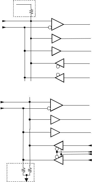
Figure 7-24. Upstream Facing Full-speed Port Transceiver
D+
 RxD
RxD
D-
Differential Receiver
 RxD+
RxD+
Single-ended Receivers
 RxD-
RxD-
|
TxD+ |
Output Buffers |
OE |
|
Speed |
|
TxD- |
Note: Additional logic is required |
|
15KΩ ±5% |
to invert signal polarity on |
|
data in/out when low-speed |
|
devices are attached. |
Figure 7-25. Downstream Facing Low-/full-speed Port Transceiver
146
Universal Serial Bus Specification Revision 2.0
7.1.7.2 Full-/High-speed Signaling Levels
The high-speed signaling voltage specifications in Table 7-3 must be met when measuring at the connector closest to the transceiver, using precision 45 Ω load resistors to the device ground as reference loads. All voltage measurements are taken with respect to the local device ground.
Table 7-3. High-speed Signaling Levels
Bus State
High-speed Differential “1”
High-speed Differential “0”
Required Signaling Level at |
Required Signaling Level at |
Source Connector |
Target Connector |
|
|
DC Levels:
VHSOH (min) ≤ D+ ≤ VHSOH (max)
VHSOL (min) ≤ D- ≤ VHSOL (max)
See Note 1.
AC Differential Levels:
A transmitter must conform to the eye pattern templates called out in Section 7.1.2.
See Note 2.
DC Levels:
VHSOH (min) ≤ D- ≤ VHSOH (max)
VHSOL (min) ≤ D+ ≤ VHSOL (max)
See Note 1.
AC Differential Levels:
A transmitter must conform to the eye pattern templates called out in Section 7.1.2.
AC Differential Levels
The signal at the target connector must be recoverable, as defined by the eye pattern templates called out in Section 7.1.2.
See Note 2.
AC Differential Levels:
The signal at the target connector must be recoverable, as defined by the eye pattern templates called out in Section 7.1.2.
|
See Note 2. |
See Note 2. |
|
|
|
High-speed J State |
High-speed Differential “1” |
High-speed Differential “1” |
|
|
|
High-speed K State |
High-speed Differential “0” |
High-speed Differential “0” |
|
|
|
147

Universal Serial Bus Specification Revision 2.0
Table 7-3. High-speed Signaling Levels (Continued)
Chirp J State
(differential voltage; applies only during reset when both hub and device are high-speed capable)
Chirp K State
(differential voltage; applies only during reset when both hub and device are high-speed capable)
High-speed Squelch State
High-speed Idle State
Start of High-speed Packet (HSSOP)
End of High-speed Packet (HSEOP)
High-speed Disconnect State (at downstream facing port)
DC Levels:
VCHIRPJ (min) ≤ (D+ - D-) ≤
VCHIRPJ (max)
DC Levels:
VCHIRPK (min) ≤ (D+ - D-) ≤
VCHIRPK (max)
NA
NA
AC Differential Levels
The differential signal at the target connector must be ≥ 300 mV
AC Differential Levels
The differential signal at the target connector must be ≤ -300 mV
VHSSQ - Receiver must indicate squelch when magnitude of differential voltage is ≤ 100 mV; receiver must not indicate squelch if magnitude of differential voltage is ≥ 150 mV.
See Note 3.
DC Levels:
VHSOI min ≤ (D+, D-) ≤ VHSOI max
See Note 1.
AC Differential Levels:
Magnitude of differential voltage is ≤ 100 mV
See Note 3.
Data lines switch from high-speed Idle to high-speed J or high-speed K state.
Data lines switch from high-speed J or K to high-speed Idle state.
NA |
VHSDSC - Downstream facing port |
|
must not indicate device |
|
disconnection if differential voltage |
|
is ≤ 525 mV, and must indicate |
|
device disconnection when |
|
magnitude of differential voltage is |
|
≥ 625 mV, at the sample time |
|
discussed in Section 7.1.7.3. |
|
|
Note 1: Measured with a 45 Ω resistor to ground at each data line, using test modes Test_J and Test_K
Note 2: Measured using test mode Test_Packet with fixture shown in Figure 7-12
Note 3: Measured with fixture shown in Figure 7-12, using test mode SE0_NACK
Note 4: A high-speed driver must never “intentionally” generate a signal in which both D+ and D- are driven to a level above 200 mV. The current-steering design of a high-speed driver should naturally preclude this possibility.
148
Universal Serial Bus Specification Revision 2.0
7.1.7.3 Connect and Disconnect Signaling
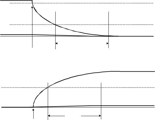
When no function is attached to the downstream facing port of a host or hub in low-/full-speed, the pull-down resistors present there will cause both D+ and D- to be pulled below the single-ended low threshold of the host or hub transceiver when that port is not being driven by the hub. This creates an SE0 state on the downstream facing port. A disconnect condition is indicated if the host or hub is not driving the data lines and an SE0 persists on a downstream facing port for more than TDDIS (see Figure 7-26). The specifications for TDDIS and TDCNN are defined in Table 7-13.
A connect condition will be detected when the hub detects that one of the data lines is pulled above its VIH threshold for more than TDCNN (see Figure 7-27 and Figure 7-28).
Hubs must determine the speed of the attached device by sampling the state of the bus immediately before driving SE0 to indicate a reset condition to the device.
All signaling levels given in Table 7-2 are set for this bus segment (and this segment alone) once the speed of the attached device is determined. The mechanics of speed detection are described in Section 11.8.2.
D+/D-
VIHZ (min)


VIL


D-/D+
VSS
|
|
|
TDDIS |
|
|
Device |
|
|
Disconnect |
||
|
|
|
|||
|
|
|
|||
Disconnected |
|
|
|
Detected |
|
Figure 7-26. |
Low-/full-speed Disconnect Detection |
||||
|
D+ |
VIH |
|
VSS |
D- |
|
|
|
TDCNN |
Device |
Connect |
Connected |
Detected |
Figure 7-27. Full-/high-speed Device Connect Detection
149
Universal Serial Bus Specification Revision 2.0
|
D- |
VIH |
|
VSS |
D+ |
|
|
|
TDCNN |
Device |
Connect |
Connected |
Detected |
Figure 7-28. Low-speed Device Connect Detection
Because USB components may be hot plugged, and hubs may implement power switching, it is necessary to comprehend the delays between power switching and/or device attach and when the device’s internal power has stabilized. Figure 7-29 shows all the events associated with both turning on port power with a device connected and hot-plugging a device. There are six delays and a sequence of events that are defined by this specification.
Hub port |
|
|
|
|
Attach Detected |
|
|
|
|
|
|
|
|
|
|
|
|
|
|
|
|
|
|
|
|
|
|
|
|
Reset Recovery |
|||||||||||
power OK |
|
|
|
|
|
|
|
|
|
|
|
|
|
|
|
|
|
|
|
|
|
|
|
|
|
|
|
|
|
|
|
|
|
|
|
|
|
Time |
|||
Hub port |
|
|
|
|
|
|
|
|
|
|
|
|
|
|
|
|
|
|
|
|
|
|
|
|
|
|
|
|
|
|
|
|
|
|
|
|
|
|
|
||
|
|
|
|
|
|
|
|
|
|
|
|
|
|
|
|
|
|
|
|
|
|
|
|
|
|
|
|
|
|
|
|
|
|
|
|
|
|
|
|||
power-on |
|
|
|
|
≥ 4.01V |
|
|
|
|
|
|
|
|
|
|
|
|
|
|
|
∆ t5 |
|
|
|
|
|
|||||||||||||||
|
|
|
|
|
|
|
|
|
|
|
|
|
|
|
|
|
∆ t4 |
|
|
|
|
|
USB System Software |
||||||||||||||||||
VBUS |
|
|
|
|
|
|
|
|
|
|
|
|
|
|
|
|
|
|
|
|
|
|
|
|
|
|
|
|
|
|
|
|
|
|
|
|
|
|
reads device speed |
||
VIH(min) |
|
|
|
|
|
|
|
|
|
|
|
|
|
|
|
|
|
|
|
|
|
|
|
|
|
|
|
|
|
|
|
|
|
|
|
|
|
|
|
||
|
|
|
|
|
|
|
|
|
|
|
|
|
|
|
|
|
|
|
|
|
|
|
|
|
|
|
|
|
|
|
|
|
|
|
|
|
|
|
|||
|
|
|
|
|
|
|
|
|
|
|
|
|
|
|
|
|
|
|
|
|
|
|
|
|
|
|
|
|
|
|
|
|
|
|
|
|
|
|
|||
VIH |
|
|
|
|
|
|
|
|
|
|
|
|
|
|
|
|
|
|
|
|
|
|
|
|
|
|
|
|
|
|
|
|
|
|
|
|
|
|
|
||
D+ |
|
|
|
|
|
|
|
|
|
|
|
|
|
|
|
|
|
|
|
|
|
|
|
|
|
|
|
|
|
|
|
|
|
|
|
|
|
|
|
|
|
or |
|
|
|
|
|
|
|
|
|
|
|
|
|
|
|
|
|
|
|
|
|
|
|
|
|
|
|
|
|
|
|
|
|
|
|
|
|
|
|
||
D- |
|
|
|
|
|
|
|
|
|
|
|
|
|
|
|
|
|
|
|
|
|
|
|
|
|
|
|
|
|
|
|
|
|
|
|
|
10ms |
|
|||
|
|
|
|
|
100ms |
|
|
|
|
|
|
|
|
|
|
|
|
|
|
|
|
|
|
|
|
|
|
|
|
|
|||||||||||
|
|
|
|
|
|
|
|
|
|
|
|
|
|
|
|
|
|
|
|
|
|
|
|
|
|
|
|
|
|
|
|
|
|
|
|
||||||
|
|
|
|
|
|
|
|
∆ t2 |
|
|
|
|
|
|
|
|
|
|
|
|
|
|
|
|
|
|
|
|
|
|
|
|
|
|
|
|
|||||
|
|
|
|
∆ t1 |
|
|
|
|
|
|
|
|
|
100ms |
|
|
|
|
|
|
|
|
|
|
|
∆ t6 |
|||||||||||||||
|
|
|
|
|
|
|
|
|
|
|
|
|
|
|
|
|
|
|
∆ t3 |
|
|
|
|
|
|
|
|
|
|
|
|||||||||||
|
|
|
|
|
|
|
|
|
|
|
|
|
|
|
|
|
|
|
|
|
|
|
|
|
|
|
|
|
|
||||||||||||
|
|
|
|
|
|
|
|
|
|
|
|
|
|
|
|
|
|
|
|
|
|
|
|
|
|
|
|
|
|
|
|
|
|||||||||
Figure 7-29. Power-on and Connection Events Timing
∆ t1 This is the amount of time required for the hub port power switch to operate. This delay is a function of the type of hub port switch. Hubs report this time in the hub descriptor (see Section 11.15.2.1), which can be read via a request to the Hub Controller (see Section 11.16.2.4). If a device were plugged into a nonswitched or already-switched on port, ∆ t1 is equal to zero.
∆ |
t2 |
(TSIGATT) This is the maximum time from when VBUS is up to valid level (4.01 V) to when a device has |
|
|
to signal attach. ∆ t2 represents the time required for the device’s internal power rail to stabilize and for |
|
|
D+ or D- to reach VIH (min) at the hub. ∆ t2 must be less than 100 ms for all hub and device |
|
|
implementations. (This requirement only applies if the device is drawing power from the bus.) |
∆ |
t3 |
(TATTDB) This is a debounce interval with a minimum duration of 100 ms that is provided by the USB |
|
|
System Software. It ensures that the electrical and mechanical connection is stable before software |
|
|
attempts to reset the attached device. The interval starts when the USB System Software is notified of a |
|
|
connection detection. The interval restarts if there is a disconnect. The debounce interval ensures that |
|
|
power is stable at the device for at least 100 ms before any requests will be sent to the device. |
∆ |
t4 |
(T2SUSP) Anytime a device observes no bus activity, it must obey the rules of going into suspend (see |
|
|
Section 7.1.7.6). |
150
Universal Serial Bus Specification Revision 2.0
∆ t5 (TDRST) This is the period of time hubs drive reset to a device. Refer to Section 7.1.7.5 and Section 11.5.1.5 for details.
∆ t6 (TRSTRCY) The USB System Software guarantees a minimum of 10 ms for reset recovery. Device response to any bus transactions addressed to the default device address during the reset recovery time is undefined.
High-speed capable devices must initially attach as full-speed devices and must comply with all full-speed connection requirements. A high-speed capable downstream facing port must correctly detect the attachment of low-speed and full-speed devices and must also comply with all low-speed and full-speed connection behaviors.
Transition to high-speed signaling is accomplished by means of a low level electrical protocol which occurs during Reset. This protocol is specified in Section 7.1.7.5.
A downstream facing transceiver operating in high-speed mode detects disconnection of a high-speed device by sensing the doubling in differential signal amplitude across the D+ and D- lines that can occur when the device terminations are removed. The Disconnection Envelope Detector output goes high when the downstream facing transceiver transmits and positive reflections from the open line return with a phase which is additive with the transceiver driver signal. Signals with differential amplitudes ≥ 625 mV must reliably activate the Disconnection Envelope Detector. Signals with differential amplitudes ≤ 525 mV must never activate the Disconnection Envelope Detector.
To assure that this additive effect occurs and is of sufficient duration to be detected, the EOP at the end of a high-speed SOF is lengthened to a continuous string of 40 bits without any transitions, as discussed in Section 7.1.13.2. This length is sufficient to guarantee that the voltage at the downstream facing port’s connector will double, since the maximum allowable round trip signal delay is 30 bit times.
When a downstream facing port is transmitting in high-speed mode and detects that it has sent 32 bits without a transition, the disconnection envelope detector’s output must be sampled once during transmission of the next
8 bits at the transceiver output. (In the absence of bus errors, the next 8 bits will not include a transition.) If the sample indicates that the disconnection detection threshold has been exceeded, the downstream facing port must indicate that the high-speed device has been disconnected. See Section 11.12.4.
7.1.7.4 Data Signaling
Data transmission within a packet is done with differential signals.
7.1.7.4.1 Low-/Full-Speed Signaling
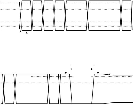
The start of a packet (SOP) is signaled by the originating port by driving the D+ and D- lines from the Idle state to the opposite logic level (K state). This switch in levels represents the first bit of the SYNC field. Hubs must limit the change in the width of the first bit of SOP when it is retransmitted to less than ± 5 ns. Distortion can be minimized by matching the nominal data delay through the hub with the output enable delay of the hub.
The SE0 state is used to signal an end-of-packet (EOP). EOP will be signaled by driving D+ and D- to the SE0 state for two bit times followed by driving the lines to the J state for one bit time. The transition from the SE0 to the J state defines the end of the packet at the receiver. The J state is asserted for one bit time and then both the D+ and D- output drivers are placed in their high-impedance state. The bus termination resistors hold the bus in the Idle state. Figure 7-30 shows the signaling for start and end of a packet.
151
Universal Serial Bus Specification Revision 2.0
VOH(min) |
|
|
||
VIH(min) |
|
|
||
VIL(max) |
|
|
||
VOL(max) |
|
|
||
VSS |
|
|
|
|
Bus Idle |
|
|
First Bit |
|
|
|
|||
|
|
|
|
|
|
SOP |
|||
|
|
|||
|
of Packet |
|||
|
|
|
||
Last Bit |
|
Bus Driven to |
|
|||||
of Packet |
|
J State at end |
|
|||||
|
|
|
|
|
of EOP |
|
||
|
|
|
|
|
|
|||
|
|
|
SE0 |
|
|
Bus |
|
|
|
|
|
|
|
|
|||
|
|
|
|
|
Floats |
|
||
|
|
|
portion |
|
Bus Idle |
|||
|
|
|
|
|
|
|||
|
|
|
|
|
|
|||
|
|
|
of EOP |
|
|
|
||
|
|
|
|
|
|
|
||
|
|
|
|
|
|
|
||
VOH(min) 


VIH(min)
VIL(max)


VOL(max)


VSS
Figure 7-30. Low-/full-speed Packet Voltage Levels
7.1.7.4.2 High-speed Signaling
The high-speed Idle state is when both lines are nominally at GND.
The source of the packet signals the Start of Packet (SOP) in high-speed mode by driving the D+ and D- lines from the high-speed Idle state to the K state. This K is the first symbol of the SYNC pattern (NRZI sequence KJKJKJKJ KJKJKJKJ KJKJKJKJ KJKJKJKK) as described in Section 7.1.10.
The high-speed End of Packet (EOP) begins with a transition from the last symbol before the EOP to the opposite symbol. This opposite symbol is the first symbol in the EOP pattern (NRZ 01111111 with bit stuffing disabled) as described in Section 7.1.13.2. Upon completion of the EOP pattern, the driver ceases to inject current into the D+ or D- lines, and the lines return to the high-speed Idle state. The high-speed SOF EOP is a special case. This SOF EOP is 40 symbols without a transition (rather than 8 for a non-SOF packet).
The fact that the first symbol in the EOP pattern forces a transition simplifies the process of determining precisely which is the last bit in the packet prior to the EOP delimiter.
152