

Interfacing with C plus plus-programing communication with microcontrolers (K. Bentley, 2006)
.pdf2 PARALLEL PORT BASICS AND INTERFACING 31
Table 2-2 Number System Conversions.
Decimal |
|
Binary |
|
Hexadecimal |
|
0 = 0x100 |
0 |
= 0x20 |
|
0 = 0x160 |
|
1 = 1x100 |
1 |
= 1x20 |
|
1 = 1x160 |
|
2 = 2x100 |
10 |
= 1x21 + 0x20 |
|
2 = 2x160 |
|
3 = 3x100 |
11 |
= 1x21 + 1x20 |
|
3 = 3x160 |
|
4 = 4x100 |
100 |
= 1x22 + 0x21 |
+ 0x20 |
4 |
= 4x160 |
5 = 5x100 |
101 |
= 1x22 + 0x21 |
+ 1x20 |
5 |
= 5x160 |
6 = 6x100 |
110 |
= 1x22 + 1x21 |
+ 0x20 |
6 |
= 6x160 |
7 = 7x100 |
111 |
= 1x22 + 1x21 |
+ 1x20 |
7 |
= 7x160 |
8 = 8x100 |
1000 |
= 1x23 + 0x22 |
+ 0x21 + 0x20 |
8 |
= 8x160 |
9 = 9x100 |
1001 |
= 1x23 + 0x22 |
+ 0x21 + 1x20 |
9 |
= 9x160 |
10 = 1x101 + 0x100 |
1010 |
= 1x23 + 0x22 |
+ 1x21 + 0x20 |
A = 10x160 |
|
11 = 1x101 + 1x100 |
1011 |
= 1x23 + 0x22 |
+ 1x21 + 1x20 |
B = 11x160 |
|
12 = 1x101 + 2x100 |
1100 |
= 1x23 + 1x22 |
+ 0x21 + 0x20 |
C = 12x160 |
|
13 = 1x101 + 3x100 |
1101 |
= 1x23 + 1x22 |
+ 0x21 + 1x20 |
D = 13x160 |
|
14 = 1x101 + 4x100 |
1110 |
= 1x23 + 1x22 |
+ 1x21 + 0x20 |
E = 14x160 |
|
15 = 1x101 + 5x100 |
1111 |
= 1x23 + 1x22 |
+ 1x21 + 1x20 |
F = 15x160 |
|
16 = 1x101 + 6x100 |
10000= 1x24 + 0x23 |
+ 0x22 + 0x21 + 0x20 |
10 = 1x161 + 0x160 |
||
17 = 1x101 + 7x100 |
10001= 1x24 + 0x23 |
+ 0x22 + 0x21 + 1x20 |
11 = 1x161 + 1x160 |
||
When developing programs, it is sometimes necessary to output digital signals through a port as one or more bytes of data. The signals to be output form binary bit patterns, which are more conveniently represented within program code as hexadecimal numbers. At other times you will need to represent incoming binary data sent from external devices as hexadecimal numbers. The following examples demonstrate the conversion of a binary number into hexadecimal.
We can obtain the hexadecimal representation for a binary number if we divide the binary number into groups of four digits starting from the least significant digit or bit (LSB, right-most digit of the number). Note that when we break a byte into two groups of four bits, we have what is termed two nibbles of data.
10001 |
= |
1 |
0001 |
|
|
(hexadecimal numbers are often |
|
|
|
|
|
|
|
|
= |
1 |
1 |
hex |
|
written using a 0x prefix , i.e. 0x11) |
1010001101 |
= |
10 |
1000 |
1101 |
|
|
|
= |
2 |
8 |
D |
hex |
(0x28D) |
Alternately, hexadecimal is denoted by using the $ or H symbols, i.e. $11 or 11H.

32 2 PARALLEL PORT BASICS AND INTERFACING
From the preceding example, if we want our program to store data at the binary address 1010001101, we would manually convert this number into hexadecimal format as 0x28D and use this hexadecimal number as the storage address in our program. Had we converted the binary number into decimal format as 653, we would need to carry out a more involved conversion.
Now we are familiar with hexadecimal representation, we can use this notation for our parallel port address. The BASE address of the parallel port is 0x378 for most PC’s, however, in some instances the parallel port uses a BASE address of 0x278, 0x3BC, or 0x300. Working with the more common BASE address of 0x378, we have the BASE+1 address of 0x379 and BASE+2 address as 0x37A.
2.4Program Demonstrating Hexadecimal to Decimal
The program shown in Listing 2-1 can be used to convert numbers from decimal to hexadecimal and vice-versa. It is often more convenient to use hexadecimal notation in program code when outputting bit patterns through the port than decimal notation. Conversely, it is at times most convenient to display on-screen, the decimal number representation for the bit patterns read in through the port. Use this program to improve your familiarity between decimal and hexadecimal number systems.
Listing 2-1 Program to display numbers in decimal and hexadecimal format.
/***************************************************** This program prints a number you would enter in decimal format in hexadecimal format.
*****************************************************/
#include <iostream.h>
void main()
{
int Number;
cout << "Enter an integer number -> "; cin >> Number;
cout << "The number is:" << endl;
cout << dec << Number << " in decimal" << endl; cout << hex << Number << " in hexadecimal" << endl;
}
In Listing 2-1, the include file iostream.h facilitates the use of cout and the number conversion argument hex. The variable, Number ,will receive the integer

2 PARALLEL PORT BASICS AND INTERFACING 33
you will pass to the program in response to the prompt “Enter an integer number -> ”. The same number is then printed on two successive lines, first in decimal format, which is the default number representation, and then in hexadecimal format. The hexadecimal format is activated by the format specifier hex.
2.5 Summary
This chapter explained the configuration of the parallel port and the digital logic concepts involved when using the port with external circuitry. These concepts include binary notation, digital logic levels, noise margins and different types of logic families such as CMOS and TTL.
The PC parallel port uses three I/O addresses to transfer data through the port’s interface. Each address controls one byte of data, however, for two I/O addresses, several data bits are unused and a few other bits are inverted internally by the port circuitry. The first I/O address is used to output data only, the second address is used to input data through the port and the last address can be used to both input and output data. Furthermore, representation of data using decimal, hexadecimal and binary number systems has been explained. This knowledge will be used when developing programs in the chapters ahead.
2.6 Bibliography
Bergsman, P. , Controlling The World With Your PC, HighText Publications, San Diego, 1994.
IBM, Technical Reference – Personal Computer AT, IBM Corporation, 1985. NS CMOS, CMOS Logic Databook, National Semiconductor Corporation, 1988.
Wakerly, J. F., Digital Design Principles and Practices, Second Edition, Prentice Hall, 1994.

3
Testing the
Parallel Port
Inside this Chapter
ξ
ξ
ξ
Simple testing of the port.
Power supply, port interface, logic buffers and driving LEDs.
C-style programming to use the entire parallel port.

3.1 Introduction
The aim of this chapter is to develop software that will enable us to see the basic input/output operations when using the parallel port of your PC. Program operation is verified using a simple test circuit with LEDs as indicators. Operation of the onboard power supply, parallel port interface and LED Driver circuits is explained before directing the reader to build these circuits. Once these circuits are built (in the order presented), programs can be written and tested.
We will start our program development by writing simple non-object-oriented programs to input and output data through the parallel port. Later on, in Chapter 5, you will be introduced to object-oriented programming (OOP). When you reach the end of this chapter, you will have seen operation of the parallel port for data transfer and you will have gained an understanding of how a simple C++ program is written.
3.2 Interface Board Power Supply
All circuitry on the interface board requires electrical power at a steady voltage in order to function properly. A power supply as part of the interface board generates the individual voltages needed by its different circuits. This section of the board should be assembled and tested first before assembling any other circuitry. You should proceed to assemble the next segment of circuitry only when the power supply is generating correct voltages.
|
|
|
|
|
|
|
|
|
Power Supply |
|
|
|
|
|
|
Mains |
|
|
|
|
+5V at < 1A |
|
Vcc |
||||||||
|
|
|
Transformer |
|
|
|
|
|
|||||||
|
|
|
|
|
|||||||||||
Supply |
|
|
|
+9V |
|||||||||||
(power point) |
|
(Power -Pack) |
|
|
|||||||||||
|
+9V at < 1A |
|
|
|
|
|
|||||||||
|
|
|
|
|
|
|
|
|
|
|
|
|
|
|
|
9V |
|
|
|
|
|
|
|
|
|
GND |
|
|
|
|
|
|
|
|
|
|
|
|
|
|
|
|
|
|
|
||
|
|
|
|
|
|
|
|
|
|
|
|
|
|
||
|
|
|
|
|
|
|
|
|
|
|
|
|
|
|
|
|
|
|
|
|
|
|
|
|
|
|
|
|
|
||
|
|
|
|
|
|
|
|
|
|
|
|
||||
|
|
|
|
|
|
|
|
|
|
|
|
|
|
|
|
Battery |
|
|
|
|
|
|
|
-8V at < 20mA |
|
|
|
|
|
||
|
|
|
|
|
|
|
|
|
|||||||
|
|
|
|
|
|
|
|
|
|
|
|
|
|
||
|
|
|
|
|
|
|
|
|
|
|
|
|
|
|
|
|
|
|
|
|
|
|
|
|
|
|
|
|
|
|
|
|
|
|
|
|
|
|
|
|
|
|
|
-8V |
|||
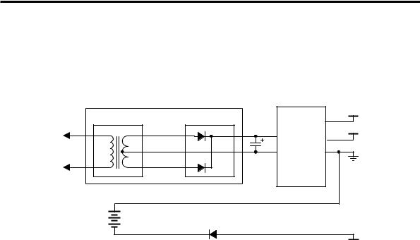
Figure 3-1 Power Supply Block Diagram.
A block diagram of the power supply is shown in Figure 3-1. Most of the power used by the interface board is supplied from the high voltage power point (known as mains supply) via the transformer (power-pack). The power supply +5V and +9V outputs can operate at their fixed voltages when supplying currents up to approximately 1A. This maximum current rating applies when the correctly rated
3 TESTING THE PARALLEL PORT 37
heatsink is fitted to each of the voltage regulators. The –8V output does not use mains supply; instead a 9V battery is used to meet its voltage and low current requirements. The –8V output powers analog circuitry which has a wide operating margin for its supply voltage, and hence there is no need for voltage regulation.
To Power Point
(AC Volts)
|
|
Voltage Regulators |
Transformer |
Rectifier |
Vcc |
+5V |
||
|
Filter |
+9V |
|
|
+9V |
|
|
GND |
Power-Pack
9V Battery
-8V
Figure 3-2 Power supply sub-circuits.
Figure 3-2 shows a more detailed functional diagram of the entire power supply. The 9V battery passes electrical energy through a diode that allows current to flow only if the battery is connected with correct polarity. When current is drawn through this circuit, the diode drops approximately 1V, producing a –8V low current power source.
The portion of the power supply using mains voltage is made up of four subcircuits: a transformer, a rectifier/filter and two voltage regulators (+5V and +9V). The combined effect of these sub-circuits is to take the alternating mains voltage and convert it into stable +5V and +9V DC voltages, free of oscillation.
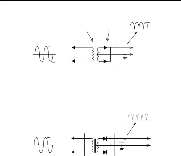
The alternating mains voltage needs to be reduced in amplitude and then rectified before it can be of use to our ‘low voltage’ circuits. The transformer inside the Power-Pack carries out this function. It has two diodes fitted inside to allow current to flow in one direction only, rectifying the sinusoidal waveform from the transformer as shown in Figure 3-3.
The voltage regulators will not function properly unless the voltage fed to their input voltage terminals is at least several volts greater than the regulator output voltage. A large value capacitor is added to the output from the power-pack to prevent its output from repeatedly dipping to zero, and instead dipping within acceptable levels as shown in Figure 3-4.
38 3 TESTING THE PARALLEL PORT
~ +12V
Transformer Diodes 0V
|
+ |
To Voltage |
|
To Power Point |
|
0 |
Regulator |
|
(AC Volts) |
|
|
|
|
|
|
_ |
|
|
|
Power-Pack |
Figure 3-3 Power-Pack Power Supply (without capacitor).


 ~ +12V
|
|
0V |
|
|
|
(reduced ripple) |
|
|
+ |
|
|
0 |
To Power Point |
Capacitor |
|
|
|||
(AC Volts) |
To Voltage |
||
|
|||
|
_ |
||
|
Regulator |
||
|
|
Power-Pack
Figure 3-4 Power-Pack Output with Capacitor added.
The voltage regulators accept a rippling input voltage as can be seen in Figure 3-5, and use their internal circuitry to steady their output voltage to within a few percent of their rated voltage. For example, the +5V regulator will produce an output voltage that lies between +4.75V and +5.25V. The voltage regulators on the interface board have several capacitors connected between their input pins and ground, and between their output pins and ground. These capacitors prevent the output of each regulator from oscillating at “high frequencies” and improve the ability of the regulator to respond to fast transient loads.

3 TESTING THE PARALLEL PORT 39
Voltage Regulator
(Stabiliser)
|
|
|
|
|
~ +12V |
|
Input |
|
|
|
|
Output |
|
|
+5V |
|
|
|
|
|
|
|
|
|
|
|
|
||||
|
|
|
|
|
|
|
|
|
|
|
|
|
|||
|
|
|
|
|
|
|
|||||||||
|
|
|
|
|
|
|
|
|
|
|
|
|
|||
0V |
|
|
|
|
|
|
Voltage |
|
|
|
|
Voltage |
|
|
0V |
|
|
|
|
|
|
||||||||||
|
|
|
|
|
|
|
|
||||||||
|
|
|
|
|
|
|
Ground |
|
|
|
|||||
|
|
|
|
|
|
|
|
|
|
|
|
|
|
|
|
|
|
|
|
|
|
|
|
|
|
|
|
|
|
|
|
|
|
|
|
|
|
|
|
|
|
|
|
|
|
|
|
Figure 3-5 Voltage Regulator (without capacitors).
The hardware for the power supply should now be assembled and tested. Appendix A contains guidance for hardware assembly, soldering, schematic diagram conventions, testing and debugging, printed circuit board preparation and checking. This material should be read before commencing with the assembly and testing of the power supply. The power supply schematic diagram, bill of materials and test instructions are also to be found in Appendix A.
3.3 Parallel Port Interface
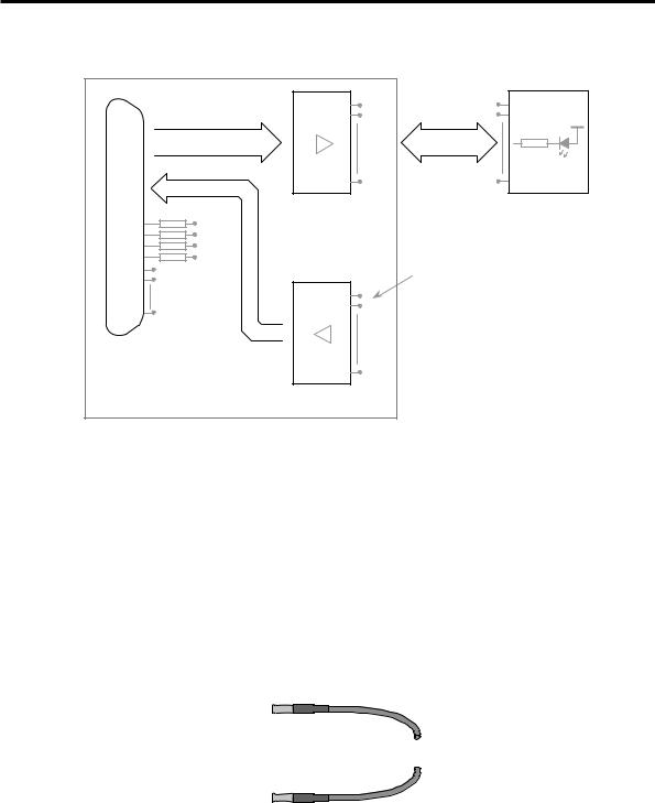
We will often need to check the correct operation of our programs during their software development cycle. The interface board has circuitry that allows us to test the functionality of the entire parallel port and thus provide feedback on program execution. A block diagram of this circuit is shown in Figure 3-6.
The signals from the parallel port are connected through the interface cable to the interface board D25 connector. From here, eight of the signals connect with a Buffer integrated circuit. These signals are generated by writing data to the BASE address. A second Buffer IC on the interface board is used to send five signals to the PC’s BASE+1 Address, via pcb tracks connected to the D25 connector. A further four signals controlled by the BASE+2 address, pass through the D25 connector to individual resistors. This part of the port can both output data or input data.
Permanent damage often occurs when output pins of IC’s are accidentally connected together without any means of limiting the resulting currents. Resistors are connected in series with BASE+2 signal lines to limit the currents and minimise damage should any of these lines from the PC be improperly connected to other outputs on the interface board.
Note that the two 8 way Buffer ICs shown in Figure 3-6 also have pull-up resistors fitted to their input pins (resistors not shown). Their function is explained in the Parallel Port Interface section of Appendix A.
40 3 TESTING THE PARALLEL PORT
Parallel Port Interface
8 wires (pcb tracks) |
BASE |
from PC) |
|
|
|
From |
(Output |
|
|
8 way Buffer IC |
|
BASE+2 (In/Out) |
(pcb tracks) |
|
|
|
wires |
ToBASE+1 |
(Input to PC) |
INTERFACE Board |
5 |
||
|
|
|
|
D25 Connector |
|
|
|
(Female) |
|
|
|
8 way Buffer IC
LED Driver Circuit
Vcc
8 interconnect leads
8 way Driver IC
8 Resistors/LEDs
Pcb Interconnect Pins
Figure 3-6 Parallel Port Interface & LED Driver Block Diagram.
The circuitry shown in Figure 3-6 has small pins with dots at their ends. These dot symbols represent printed circuit board pins that allow interconnection between other circuits on the board. This is made possible by using an interconnecting lead (shown in Figure 3-7) to connect between pins. You can fabricate these leads as required by following the instructions given in Appendix A.
Each connection made with an interconnecting lead connects an output pin of a circuit to an input pin of another circuit. DO NOT at any time connect outputs pins to other outputs pins. Doing so will most likely damage the components involved.
25 cm
Figure 3-7 Interconnecting Lead.

3 TESTING THE PARALLEL PORT 41
Also shown on the diagram of Figure 3-6, is a resistor and light emitting diode (LED), representative of a group of eight such devices. This circuit is used to indicate the state of data coming from the PC or the interface board itself. Check the data generated within the interface board by connecting the relevant output pins of the circuit to individual resistor and LED pairs.
To test programs that read data into the PC through the parallel port, the interface board has a number of pcb pins permanently connected to either +5V or GND. This arrangement allows us to test any of the four or five input bits of the PC parallel port that use BASE+1 and BASE+2 addresses respectively.
Proceed to assemble the parallel port hardware and test for correct operation. Appendix A contains the schematic diagram, hardware assembly and test instructions for this circuitry. Several interconnect leads will need to be made for test purposes.
3.3.1 LED Driver Circuit
Figure 3-6 shows eight logic outputs (that originate from the parallel port) connected to a Buffer via pcb tracks. Unfortunately, like most digital logic circuits, a single logic output from the parallel port circuit does not have the capacity to pass sufficient current through a LED; hence the need for the Driver IC. Each output pin from the Buffer is connected to an individual pcb pin. The interconnect lead wires connect the Buffer output pins to the input pins of the LED Driver IC.
The Driver used on this board has the part number ULN2803A. It houses a bank of internal transistors, each one well suited to accept the limited current from a logic output pin and then to drive a LED. Most LEDs require between 5mA and 20mA of current through them to glow with adequate brightness. The ULN2803A Driver switches current flow independently through each of the eight LEDs and resistors, and operates as follows:
1.When a Driver input pin (on the left side of the Driver) is taken to a high voltage level, the corresponding output pin is switched internally to ground voltage. This allows current to flow from Vcc (equal to +5V), through the LED, and resistor, and through the Driver output pin to ground, causing the LED to glow.
2.When the Driver input is driven to a low voltage level, the corresponding output pin connection path to GND will become highly resistive. This reduces current flow through the LED and resistor to extremely low levels and extinguishes the glow of the LED.
3.3.2 LED Operation
A minimum amount of current needs to flow through a light emitting diode (LED) for it to light. LEDs, like most diodes, conduct significant levels of current in one direction only during normal operation. The current flows from the anode (denoted by a triangle) to the cathode (denoted by a bar) as shown in Figure 3-8.