

Interfacing with C plus plus-programing communication with microcontrolers (K. Bentley, 2006)
.pdf1 GETTING STARTED 21
|
|
Function A |
2 |
|
|
(reads Data A) |
|
|
|
|
|
|
1 |
3 |
Data A |
|
|
||
|
|
|
|
|
7 |
|
|
Function C |
main( ) |
|
|
(reads then |
|
|
|
writes Data B) |
10 |
|
|
|
|
4 |
|
9 |
|
6 |
Function B |
|
|
|
|
8 |
|
|
(writes Data B) |
|
|
|
|
|
Data B |
5 |
|
|
|
|
|
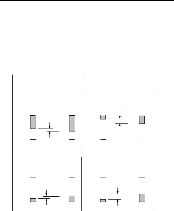
Figure 1-14 Program with main()function, other functions and data.
1.7 Summary
Program development software is typically used to write C++ programs. This software provides an integrated environment for editing, compiling and linking programs. Built-in libraries known as Run-Time Libraries are part of the development environment and contain useful functions. To use these functions, header files are included at the start of the program to provide the respective function declarations.
A C++ program comprises the code written using correct syntax, comments, keywords, identifiers, fundamental data types, user-written data types and header files. Keywords are the reserved words that are part of the C++ language. Fundamental data types are built-in data types +and can be used to develop more complex user-written data types. Identifier names are chosen by the programmer and must not be C++ keywords. Both identifiers and functions must be declared ahead of their use in a program.
C++ programs carry out procedures by using functions that operate on specific data. This simplifies programming since the programmer only calls the function to perform a task and does not need to know how the function implements the call (this is procedure abstraction). A special type of function named main starts and ends program execution. Functions can return a value from within their body after carrying out their assigned operations. The type of this data must be specified at the time of defining the function, therefore, the function has what is known as a return

22 1 GETTING STARTED
value type. In addition to this, functions often require input data in order to carry out their dedicated operations. This input data is passed into functions with the use of their function parameters.
Early in this chapter we explained a basic C++ program comprising just the main() function. An additional function was then added to this program to carry out the same task and demonstrate procedure abstraction. Finally, a program was presented and discussed that added two numbers using a function that had parameters and a return value.
1.8 Bibliography
Kelley, A. and I. Pohl, A Book on C – programming in C, Benjamin Cummins, 1995.
House, R., Beginning with C – An Introduction to Professional Programming,
International Thompson Publishing, 1994.
Deitel H.M. and P.J. Deitel C: How to Program, Prentice Hall, 1994.

2
Parallel Port
Basics and
Interfacing
Inside this Chapter
ξ
ξ
ξ
ξ
Parallel port configuration & functionality.
Digital logic fundamentals.
Number systems: decimal, hexadecimal and binary.
Electronics: port, byte, synchronous, asynchronous, addresses.
2.1 Introduction
A basic understanding of digital logic principles and converting data between number systems is needed before the parallel port can be used effectively. This chapter covers these topics and also describes the configuration of the parallel port itself. Concepts such as binary logic, logic levels, input/output address space and the physical connection to the port will be explained.
Working through this chapter will prime you for programming and connecting to the parallel port. You will use this knowledge in future chapters when developing programs to control and monitor hardware through the port. An understanding of basic electronic logic principles is also beneficial when constructing and testing many circuits on the interface board.
2.2 What is the Parallel Port?
Generally speaking, a port is a portion of electronic hardware that is used as an interface to connect with another electronic device for the purpose of information exchange. This connection allows information in the form of data to flow into, out of, or both into and out of the port.
The parallel port has the facility to transfer data both in and out, between the PC and the outside world. It is normally used for sending information to a printer and also known as the printer port. With older computers, the printer port is made up of circuitry residing on a separate printed circuit board (referred to as a pcb) which plugs into the PC motherboard. Newer computers, however, tend to have the parallel port circuitry integrated along with the rest of the PC motherboard.
Having a basic familiarisation with concepts such as logic families, logic levels and noise margins helps to be able to gain an understanding how electronic devices communicate digitally. This understanding will also prove useful should electrical problems arise when using digital circuitry on the interface board.
2.2.1 Digital Logic
As mentioned earlier, computer programs are executed by hardware which operates using binary logic, also known as digital logic. Binary logic has two possible states, ON and OFF. Typically these binary logic states are represented using binary logic notation, where 1’s denote the ON state and 0’s denote the OFF state.
The ON and OFF states used by the parallel port circuitry and many other digital logic circuits are implemented using voltage levels known as logic levels which commonly lie between 0V and +5V. Note that not all types of logic circuits use the same logic voltage levels. These logic circuits are also known as integrated circuits (IC’s), containing groups of circuit elements housed on a single piece of semiconductor material known as a “chip”. The chip is packaged inside either
2 PARALLEL PORT BASICS AND INTERFACING 25
plastic or ceramic material with metal leads that are bonded internally with wire to the chip to allow external connection.
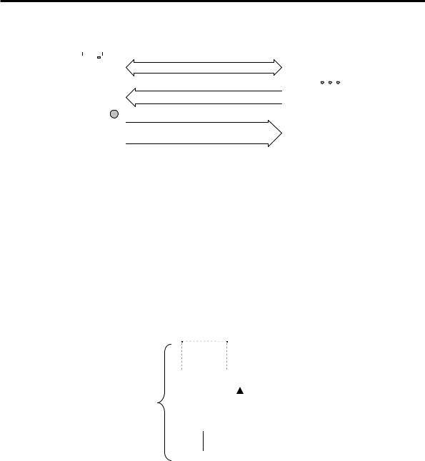
The two most popular types of logic circuit or logic families are TTL (transistor transistor logic) and CMOS (complementary metal oxide semiconductor). Each logic family is fabricated in a unique way, resulting in distinctive electrical operating characteristics. Some basic electrical differences between TTL and CMOS logic families are shown in Figure 2-1. There are several different versions for each family, with characteristic variations in electrical specification.
Note that some CMOS logic families can operate at voltages outside the 0V to +5V range shown. Also, the output voltage level for these circuits does depend on the level of current drawn through each output.
TTL (transistor transistor logic) |
|
CMOS (complementary metal oxide |
||
|
semiconductor) |
|||
|
|
|
||
|
|
|
|
|
|
a) |
|
|
b) |
|
|
|
|
|
Output Level (sending) |
Input Level (receiving) |
|
Output Level (sending) |
Input Level (receiving) |
Logic-HIGH or One |
Logic-HIGH or One |
|
Logic-HIGH or One |
Logic-HIGH or One |
+5V |
+5V |
+5V |
+5V |
|
Noise |
|
|
|
4.7V |
+3.2V |
|
|
Margin |
|
|
+2.4V |
+2.0V |
|
Noise |
|
Margin |
||
|
|
||
|
|
|
0V |
0V |
0V |
0V |
|
c) |
|
|
d) |
|
|
|
|
|
Output Level (sending) |
Input Level (receiving) |
|
Output Level (sending) |
Input Level (receiving) |
Logic-LOW or Zero |
Logic-LOW or Zero |
|
Logic-LOW or Zero |
Logic-LOW or Zero |
+5V |
+5V |
+5V |
+5V |
|
Noise |
|
Noise |
|
|
|
Margin |
||
|
Margin |
|
||
|
|
+1.5V |
||
+0.4V |
+0.8V |
|
||
+0.2V |
|
|||
|
|
|||
0V |
0V |
0V |
||
0V |
Figure 2-1 Typical CMOS and TTL logic voltage levels (5V supply).
These differences in logic levels from one family to the other are very significant when connecting between them. For example, referring to Figure 2-1 quadrants a)

26 2 PARALLEL PORT BASICS AND INTERFACING
and b); consider the case where a TTL integrated circuit sends a HIGH logic level (+5V to +2.4V) to a CMOS integrated circuit. In this case, the TTL circuit could, at worst, send (output) a logic-HIGH having +2.4V, the lowest output voltage level when operating normally (not damaged or being over-driven). If the CMOS circuit is to correctly recognise a received (input) logic-HIGH level, this received voltage must be at least +3.2V and no more than +5V. The problem with this situation is that the TTL integrated circuit can output a signal down to +2.4V, too low a voltage level for the CMOS integrated circuit to accept as a valid logic-HIGH. The result could be that the CMOS circuit incorrectly mistakes the TTL HIGH level as a LOW level.
Figure 2-1 also shows the voltage noise margin when a data signal is sent from one logic circuit to another of the same family. Let us look at the case in which a CMOS circuit outputs a logic-LOW to another CMOS circuit, as shown in quadrant d) of the figure. The sending device will output a signal between 0V and 0.2V during normal operation and the receiving device will accept a signal level between 0V and 1.5V as a valid logic-LOW. If we use an output signal of 0.2V, the worst case for normal operation, then we can have voltage noise of up to 1.3V (1.5V – 0.2V) on this logic signal, and the receiving circuit will still recognise a valid logic-LOW. From this example we can see we have a noise margin of 1.3V.
If you examine the same case shown in quadrant c) for a TTL circuit transmitting a logic-LOW to another TTL circuit, you will find that there is a noise margin of only 0.4V. CMOS circuits typically have better noise margin characteristics than TTL circuits. Other differences between TTL and CMOS circuits include their power consumption, their input current requirements, and their output current drive capacity and speed when switching states. For additional information concerning digital logic families, consult the references at the end of this chapter.
2.2.2 Parallel Port Architecture
The parallel port allows print data to be sent from the PC to the printer and data indicating printer status to be received by the PC. This data, sent by the PC, uses eight wires, to transmit a byte of information to the printer. A byte is simply a group of eight bits used together to make a unit of data. Each wire is used to transmit one bit of data at a time. Each bit of data can have one of two possible logic values, 1 or 0. Another nine wires are used to allow the PC to determine the state of the printer and control the flow of data. These nine lines are broken into a set of five input lines and four input/output lines as shown in Figure 2-2.
The physical connection to this port is through a 25-pin connector known as a ‘D25F’ connector (where the ‘D’ refers to the shape of the connector body). The 25 contacts making up this connector are all sockets (female type, hence the ‘F’ in ‘D25F’) which mate with the printer cable connector having 25 pins (male type).
2 PARALLEL PORT BASICS AND INTERFACING 27
PC (Parallel Port) |
|
|
Printer |
|||||||
|
|
|
|
|
|
|
|
|
|
|
|
|
|
|
|
|
|
|
|
|
|
|
Input/Output |
|
4 wires |
|
|
|
||||
|
BASE+2 Address |
|
|
|
|
|
||||
|
|
|
|
Input |
|
5 wires |
|
|
|
|
|
|
|
|
|
|
|
|
|||
|
BASE+1 Address |
|
|
|
|
|
||||
|
|
|
Output |
|
8 wires |
|
|
|
||
|
|
|
|
|
|
|
||||
|
|
|
|
|
|
|
||||
|
|
|
|
|
|
|
||||
|
|
|
|
|
|
|
||||
|
|
|
|
|
|
|
||||
|
|
BASE Address |
|
|
|
|
|
|||
|
|
|
|
|
|
|
|
|
|
|
Figure 2-2 Parallel Port Configuration.
The three sets of wires shown in Figure 2-2 show the connection between a PC’s parallel port and an external device, in this case a printer. Each group of wires are controlled, or read, by accessing three sequential locations in the PC’s Input/Output address space, abbreviated to I/O address space. This address space is made up of a number of data storage locations used to allow intercommunication with input/output devices. It is different from the memory generally used by the computer. The PC writes data to particular I/O addresses, where the data is stored and can be accessed by external devices. Other I/O addresses are used to allow external devices to write data into storage for the PC to read, and still other I/O addresses allow bi-directional data transfer.
|
|
|
|
I/O Addresses |
BASE + 2 |
|
|
|
|
||
|
|
|
|
BASE + 1 |
|
Increasing |
|
|
|
||
|
|
|
order |
|
BASE |
||
|
|
|
|
|
|
|
|
|
0 |
1st Address |
|
Figure 2-3 I/O Addressing.
The first of the three I/O addresses is referred to as the BASE address as shown in Figure 2-3. It is the lowest address and is used as a reference from which to increment to the other two I/O addresses belonging to the parallel port. Writing to the BASE address will output eight bits of data (a byte) from the parallel port (see Figure 2-2), where each bit uses an individual wire.

28 2 PARALLEL PORT BASICS AND INTERFACING
The next address in this block has a numerical value one more than the BASE address, so we label it the BASE+1 address. The BASE+1 address has access to the five input data bits to the PC. This address can only be used to read the state of these five signals.
The third address of this set is labelled the BASE+2 address, being two addresses past the BASE address. This address location is used to control the four bidirectional data bits of the port. Using this address, we can read and write to these four bits.
NOTE
Beware: the four BASE+2 lines used for input and output are NOT ‘strict’ logic
outputs. The parallel port interface often has resistors and capacitors connected to these lines to reduce the influence of electrical noise. This causes their states to change much slower than a strict logic output, meaning that erroneous recognition
of data can occur when connecting with certain types of logic families.
In addition, due to variation in the individual capacitor values, these signals do not
switch at ‘exactly’ the same time (synchronously). This non-synchronous
(asynchronous) switching of BASE+2 outputs can cause data transfer problems
with data interfaces designed to work synchronously.
Table 2-1 provides a summary of the data bits and D25 connector pins that the parallel port connector uses for each of the three port addresses. Each wire in the cable linking the port to the external device (usually a printer), carries the signal of a particular data bit for that port address. The BASE and BASE+2 addresses have their data bits commencing from D0 upwards. The BASE+1 address, however, starts at data bit D3.
Some data bits used by BASE+1 and BASE+2 addresses are inverted by the parallel port circuitry. These inverted bits are marked by a “ / ” character preceding the letter “D” of that bit. This signal convention is also used on the interface board schematic diagrams which show detailed electrical interconnections. When using these data bits, the program must compensate for this inversion in order that signals are output from the port or read in through the port as intended.
If a program needs to send a data bit out as a signal through one of the port’s inverted bits, it needs to invert that data bit in software beforehand. This double inversion (once in hardware and again in software) has the effect of correcting the signal back to the intended state. Likewise, when a signal is read through an inverted bit of the port, the now inverted signal must be inverted once more by the program to correct it. The program implements this inversion using one simple line of code, explained in Section 3.6 of the next chapter.
2 PARALLEL PORT BASICS AND INTERFACING 29
Table 2-1 Parallel Port D25 Connector Pin Assignment.
BASE Address |
BASE +1 Address |
BASE+2 Address |
(8-bit output data) |
(5-bit input data) |
(4-bit input/output data) |
D0 - pin 2 |
|
/D0 - pin 1 |
D1 - pin 3 |
|
/D1 - pin 14 |
D2 - pin 4 |
|
D2 - pin 16 |
D3 - pin 5 |
D3 - pin 15 |
/D3 - pin 17 |
D4 - pin 6 |
D4 - pin 13 |
|
D5 - pin 7 |
D5 - pin 12 |
|
D6 - pin 8 |
D6 - pin 10 |
|
D7 - pin 9 |
/D7 - pin 11 |
|
Note: “/ ” denotes the signal bit is inverted internally by the parallel port circuitry.
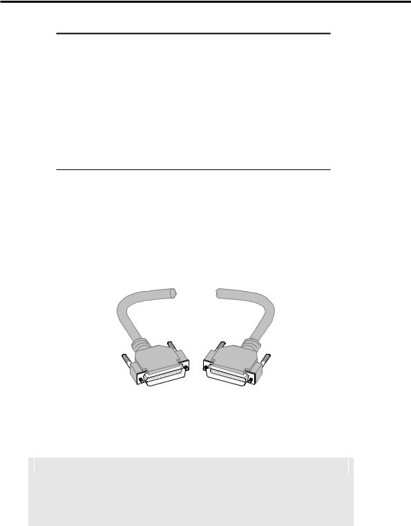
D25 pin numbers 18 to 25 are not shown in Table 2-1. They are all connected to the PC electrical ‘ground’ which is connected to the interface board through the interface cable (Figure 2-4). This cable has a D25 male connector at both ends, connected by individual wires in a “one-to-one” arrangement (D25 pin 1 of one connector to the D25 pin 1 of the other connector; likewise for all remaining pins).
2 metres
D25 Male |
D25 Male |
Figure 2-4 D25M to D25M Cable.
NOTE
Data bits D0 to D2 of BASE+1 address are not connected to the parallel port
circuitry inside the PC. The same holds true for D4 to D7 of the BASE+2 address.
Reading these particular bits will produce invalid data.

30 2 PARALLEL PORT BASICS AND INTERFACING
2.3 Data Representation
As mentioned previously, computers use ‘ON’ and ‘OFF’ states (high and low voltages) to store data, termed binary data since we have only two states. This leads to the representation of numbers using the binary (on/off) number system. The binary system is based on raising the number two to increasing integer powers to form higher and higher digit values. We can see how such a system works by comparing it with our familiar decimal number system. Decimal numbers are based on raising the number ten to higher and higher integer powers.
For example, the decimal number 25 is broken down as follows:
25= 2x101 + 5x100 = 2x10 + 5x1
Decimal 25 is equivalent to the binary number of 11001 as follows: 11001 = 1x24 + 1x23 + 0x22 + 0x21 + 1x20
=1x16 + 1x8 + 0x4 + 0x2 + 1x1
=25 (decimal)
NOTE
The binary digit to the far right has the lowest weighting and is known as the least
significant bit (LSB). Conversely, the left-most binary digit has the highest weighting and is termed the most significant bit (MSB).
Binary numbers with many digits are not easy to read. To solve this problem we use a more convenient number representation named hexadecimal. This system is based on sixteen number states.
The decimal number system uses ten unique Arabic numerals being 0, 1, 2, …, to 9. In hexadecimal representation we need sixteen unique numerals. The first ten hexadecimal digits use Arabic numerals 0, 1, 2, ..., to 9, however, we must use unique digit representation for the remaining numbers ten to fifteen. This is done by using capital letters A, B, C, D, E and F to represent ten, eleven, twelve, …, to fifteen.
Table 2-2 illustrates numerical conversion between decimal, binary and hexadecimal numbers.