

Interfacing with C plus plus-programing communication with microcontrolers (K. Bentley, 2006)
.pdf5 OBJECT-ORIENTED PROGRAMMING 103
address BASE+1. The next line calls the default constructor of the object class ParallelPort to instantiate the object named OurPort. This object has member data and member functions to write or read data to and from all three ports of the parallel port.
The remaining statements of the main() function carry out a number of output and input operations. The getch() functions are used to make the program wait for a key press to allow the user to read the screen. If the getch() statements were omitted, the screen would scroll up or revert back to the IDE before the user could see the results. The getch() function is not a member function of the object OurPort. Therefore, it is not attached to this object and as such is called as a normal function.
5.8 Summary
At the start of this chapter we developed an object class with the name ParallelPort. This class contained only sufficient data members and member functions to give us basic use of the port. We applied particular access attributes to the class members and explained the importance of making proper use of these access attributes.
Several programs were used to explain the relationship between multiple constructors and the default constructor. The ParallelPort class was then expanded to include use of the BASE+1 and BASE+2 addresses. The operation of objects instantiated from this expanded class was demonstrated using a program which transferred data to and from the interface board. Now that we have a fully functioning ParallelPort class, we will be able to use it extensively in future chapters.
5.9 Bibliography
Borland, Borland C++ Getting Started, Borland International, 1991. Winston, P.H., On to C++, Addison Wesley, 1994.
Lipman, S.B., C++ Primer, Addison Wesley, 1991.
Dench, D. and B. Prior, Introduction to C++, Chapman and Hall, 1994.
Etter, D.M., Introduction to C++ - For Engineers and Scientists, Prentice Hall, 1997.

6
Digital-to-Analog
Conversion
Inside this Chapter
ξ
ξ
ξ
ξ
ξ
ξ
Digital-to-analog conversion explained.
Generate voltages using a Digital-to-Analog Converter (DAC).
Operational amplifier basics.
Inheritance and derived classes.
Object class for the DAC.
Access specifiers.

6.1 Introduction
Digital-to-Analog Converters (DAC) form an integral part of many automated control systems. This chapter describes the principle of operation of a DAC and its typical use to produce an analog voltage or current.
You will learn how new classes are derived from existing classes during the development of software to drive a DAC. The new classes will inherit the existing functionality, have extra functionality added, and the inherited functions will be modified. In the course of this process, access attributes and access specifiers will be further explained.
6.2 Digital-to-Analog Conversion
Digital-to-analog conversion is the generation of an analog voltage or current by using a group or sequence of digital logic levels to set the state of an analog output as shown in Figure 6-1. Some types of digital-to-analog converters (DACs) use digital data presented to the DAC in a serial format, and others use digital data presented in a parallel format.
Digital Logic Levels |
Digital–to-Analog Converter |
|
Analog Output |
|
|
||
(DAC) |
|
(Voltage or Current) |
|
|
|
||
|
|
|
|
Figure 6-1 Digital-to-Analog Conversion.
There are several types of digital-to-analog converter in use. Some take in a digital pulse-train and use integration to give an analog voltage (for example, frequency to voltage converters). Other DACs use the popular method of digital- to-analog conversion discussed in this text like the DAC in this chapter’s project. In order to appreciate how the DAC operates, we need to understand a little about its main building block, the operational amplifier.
6.2.1 Operational Amplifier Basics
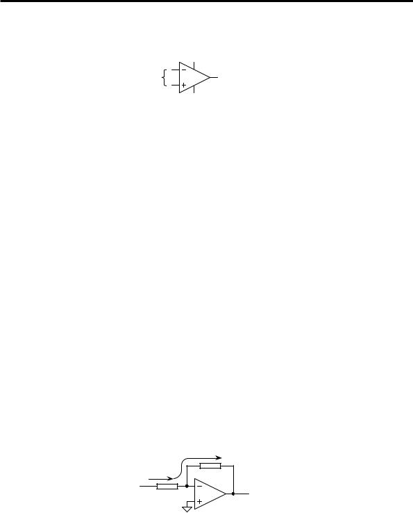
The operational amplifier is a fundamental building block for many analog electronic systems. The schematic symbol for an operational amplifier (op-amp) is shown in Figure 6-2.
6 DIGITAL-TO-ANALOG CONVERSION 107
Upper power supply voltage
V |
Vout |
Lower power supply voltage
Figure 6-2 Operational amplifier (op-amp) schematic representation.
The operational amplifier component is a very high internal gain amplifier that only needs a minute amount of current to flow through its input pins (marked with a + and – sign), in order to function. The –ve input is referred to as the inverting input and the +ve input is referred to as the non-inverting input. The device also has power supply rails (normally hidden) that connect to the upper and lower power supply voltages to power the device. When the polarity of the input voltage differential V is positive, with the +ve input voltage higher than the –ve input voltage, the op-amp output voltage (Vout) will be positive. Likewise the reverse holds true when the polarity of V is negative.
Since the op-amp internal gain is very high, say 1 million, then if a 10V output signal was to be generated, only 10/millionth of a volt is required between the two input pins ( V = 10ΠV, Π represents micro, which is 10-6). The current entering the op-amp is extremely low, and might be say 200nA (n represents nano, 10-9).
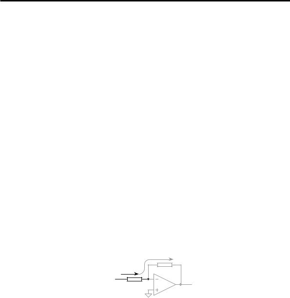
The op-amp is a building block for various amplifier designs. The two rules concerning its very high gain and practically zero input current allow us to evaluate many op-amp circuits. The op-amp shown previously in Figure 6-2 has no external components connected to it. In this state it is of no practical use, so we must connect external components from the output to the input and take advantage of what is known as a feedback configuration. The term feedback is used because we are feeding the output signal back into the input of the op-amp. Now let us look at a current-to-voltage circuit as shown in Figure 6-3, since its function is fundamental to the operation of the DAC on the interface board.
|
|
i |
Vin |
i |
Rf 2K |
|
|
|
(1V) |
Ra 1K |
Vout |
|
Figure 6-3 Current-to-voltage op-amp circuit.
108 6 DIGITAL-TO-ANALOG CONVERSION
The input voltage Vin, generates a current i which flows through the resistors Ra and Rf as shown, generating voltage Vout. We calculate the output voltage Vout by knowing the value of the current i and also the value of the voltage at the –ve input pin (and of course knowing the values of the two resistors Ra and Rf).
Vout cannot fall outside the op-amp’s power supply voltage range, since the opamp doesn’t have any special internal circuitry to generate output voltages exceeding that of the power supply. Most op-amps are powered from upper supply voltages of +15V or less and lower power supply voltages of –15V or higher. Bearing this in mind, along with the fact that the op-amp has huge internal gain, then no matter what the output voltage of the op-amp might work out to be, the difference in voltage between the +ve and –ve input pins ( V) must be less than say fifteen microvolts.
Vout (max) |
= |
V x Internal Gain |
+/- 15V |
= |
15ΠV x 106 |
In the above example, the output voltage, Vout, cannot exceed either supply voltage at +/-15V, therefore V will always be less than ~15ΠV, assuming the opamp internal gain is one million.
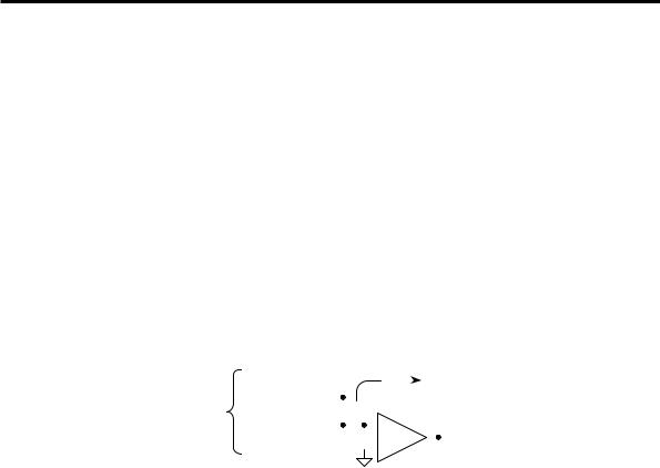
The voltage at the –ve input pin is equal to the voltage at the +ve input pin plus V. Since the voltage at the +ve input pin is equal to analog ground (0V, shown by the hollow triangle symbol), and we know that the difference in voltage ( V) between the +ve and –ve input pins will always be less than 15ΠV, the voltage at the –ve input pin will be less than 0V + 15ΠV = 15ΠV. This –ve input pin voltage is so close to zero volts that we might as well call it zero volts or virtual ground. Now that we know the –ve input pin voltage, we can calculate the current flow i and determine the output voltage Vout.
|
|
|
i |
Vin |
i |
|
Rf 2K |
|
|
|
|
(1V) |
Ra 1K |
‘0V’ |
Vout |
|
Figure 6-4 Calculating input current i.
Current flows from higher voltages to lower voltages, therefore, the current i will flow as shown in Figure 6-4 since Vin is at a greater voltage than the –ve input pin of the op-amp at virtual ground (# 0V). With 1V at one end of resistor Ra and ‘zero’ volts at the other end, the current i is as follows:

6 DIGITAL-TO-ANALOG CONVERSION 109
Current i = Volts / Resistance
=(1V – 0V) / 1K
=1mA
Note that the symbol ‘K’ represents one thousand ohms.
Since effectively zero current flows into the op-amp input pins, all of current i must flow through Rf, into the output pin and to the op-amp load (not shown).
Vout is equal to the voltage at the –ve input pin plus whatever the voltage is across resistor Rf. Using V = I x R, the voltage across resistor Rf is equal to current i multiplied by the resistance of Rf.
VRf = 1mA x 2K
=2V
As mentioned previously, current flows from higher voltages to lower voltages, therefore the voltage at the left end of Rf is at a higher voltage than the voltage at the right end of Rf. Since the left end of Rf is at 0V, the voltage difference VRf is 2V, the right end of Rf must be at –2V. Knowing that the right end of Rf is connected to Vout, Vout must be equal to –2V.
The current i flowing through the feedback circuit must enter the junction at the opamp output and split, part-of this current flowing into the op-amp load (not shown, towards Vout) and the remainder flowing into the op-amp output. How the op-amp draws the right amount of current into its output will be understood once the operation of negative feedback is explained.
In principle, the op-amp will draw (sink) or supply (source) sufficient current to ensure that current i remains at a level to force the –ve input pin to ‘0V’. This process happens automatically when a negative feedback configuration is used, as shown in Figure 6-3 and Figure 6-4. To configure negative feedback, connect the output voltage Vout back to the –ve input, either directly or through the use of external components, usually resistors. Negative feedback works as follows.
If say, the input voltage Vin increases, the voltage at the –ve input will increase slightly, increasing the small negative voltage difference between the op-amp’s +ve and –ve inputs ( V). This increased negative voltage ( V) will generate an increasingly more negative output voltage Vout, which will in-turn have the negative effect of reducing the voltage at the –ve input pin. This generates a decrease in V that will eventually settle to equilibrium. This process takes place automatically and quite rapidly in the op-amp when using negative feedback.
Positive feedback, on the other hand is altogether different and does not produce a self-correcting output voltage. Instead, the output voltage swings to the appropriate voltage supply. Later when the polarity between the +ve and –ve inputs is reversed, the output will swing to the opposite voltage supply. This type of feedback is used inside voltage comparators.
Armed with an understanding of how a current-to-voltage converter circuit works, we can move on to analyse and understand how practical DAC circuitry works.
110 6 DIGITAL-TO-ANALOG CONVERSION
6.2.2 DAC Circuit Principles
Two DAC methods will be discussed that use a group of parallel digital inputs to generate an analog output voltage. Both methods use current-to-voltage conversion as discussed in the preceding section. The two methods differ in the configuration of their logic input resistor arrays. The first method discussed is the summing amplifier DAC.
6.2.2.1 Summing Amplifier DAC
This circuit (shown in Figure 6-5) operates under the same principle as the current- to-voltage amplifier circuit shown in Figure 6-3 and Figure 6-4 earlier. Previously one input resistor was used to generate the current iT, whereas in this case the summing amplifier uses four input resistors, each resistor generating its own input current. For the summing amplifier, the individual currents flowing out of each input resistor add together to form iT.
|
20 |
|
|
|
|
|
|
|
|
|
|
|
|
|
|
|
iT |
||||||
|
|
R0 16K |
|
|
|
|
|
|
|||||||||||||||
|
21 |
|
|
|
|
|
|
|
|
|
|
|
|||||||||||
|
|
|
|
|
|
|
|
|
|
|
|
|
|
|
|
|
|
|
|
|
|
|
|
Logic Inputs |
|
|
|
|
|
R1 8K |
|
|
|
|
Rf 1K |
|
|
||||||||||
(0V or +5V) |
22 |
|
|
|
|
|
|
|
|
|
|
|
|
|
|
|
|
|
|
|
|
|
Vout |
|
|
|
|
|
R2 4K |
|
|
|
|
|
|
|
|
|
|
|
|
||||||
|
23 |
|
|
|
|
|
|
|
|
|
|
|
|
||||||||||
|
|
|
|
|
|
|
|
|
|
|
|
|
|
|
|
|
|
|
|
|
|
|
|
|
|
|
|
|
|
R3 2K |
|
|
|
|
|
|
|
|
|
|
|
||||||
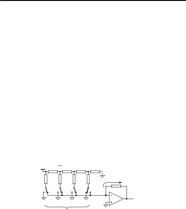
Figure 6-5 Summing amplifier DAC.
If all four input resistors were the same resistance value, each would be able to contribute either zero current (logic zero input) or ¼ of the total current iT (logicHIGH input). Therefore, the DAC output could have the following states:
DAC Output |
0V |
(all logic inputs at 0V) |
|
-1V |
(one logic input +5V, others 0V) |
|
-2V |
(two logic inputs +5V, others 0V) |
|
-3V |
(three logic inputs +5V, other 0V) |
|
-4V |
(all logic inputs +5V) |
Having all four resistors with identical resistance will only give us five output states with 1V steps. Knowing that four unequally weighted logic bits can form sixteen unique numbers, we change the resistance values accordingly to achieve sixteen unique current levels of iT. Input resistors R0, R1, R2 and R3 are chosen such that their input resistance values differ by a power of two from one resistor to the next.
Resistor R0 contributes the equivalent of the binary number 20, R1 is equivalent to 21 etc., as shown in Figure 6-5. The current derived from the 20 logic input will be 1/8 th that of the 23 logic input, the current from the 21 logic input will be ¼ that of
6 DIGITAL-TO-ANALOG CONVERSION 111
the 23 logic input and the current from the 22 logic input will be ½ that of the 23 logic input. By using the various combinations of logic input states, sixteen different combined current levels can be generated, resulting in sixteen different output voltages.
This DAC method has a drawback; to implement a DAC with finer voltage resolution (a larger number of logic input bits), requires more accurate resistor values. For example, an 8-bit DAC (having 256 states) would need to have resistance tolerances of much less than 1/256 in order to avoid over-stepping between states within the whole DAC output range. Also, the actual values of these resistors will be non-standard – more difficult to achieve. The following circuit known as a R-2R ladder avoids these problems.
6.2.2.2 R-2R Ladder DAC
This circuit also uses current-to-voltage conversion like the Summing Amplifier DAC. The difference between these two methods is the configuration of the input resistor arrays.
The input voltage to the resistor array is a very stable and precise voltage reference, marked as VREF in Figure 6-6. This is needed to allow the generation of accurate current levels to flow through the circuit. If you examine the R-2R circuit, you will see four switches (actually semiconductor switches), each switch individually controlled by one of the four logic inputs. The switches connect with either the analog ground (shown by the symbol) at 0V, or they connect with the op-amp –ve input pin at virtual ground. The term virtual ground is used because this pin is nearly at 0V (as described previously in Section 6.2.1). Realising that the switches will connect with 0V in either switch position, the R-2R resistor array can be analysed as follows.
|
|
|
VREF |
|
|
VREF |
|
|
VREF |
|
VREF |
|
R |
2 |
|
R |
4 |
|
R |
8 |
2R |
|
|
|
|
|
|
|||||
2R |
|
|
2R |
|
|
2R |
|
|
2R |
iT |
|
|
|
|
|
|
|
|
|
|
Rf |
0 |
1 |
|
0 |
1 |
|
0 |
1 |
|
0 |
1 |
23 |
|
|
22 |
|
|
21 |
|
|
20 |
Vout |
|
|
|
|
|
|
|
||||
Logic Inputs |
control the ‘switches’ |
|||||||||
Figure 6-6 R-2R ladder DAC.
The current flowing through the switch controlled by the least significant bit, 20 is 1/8th of the current flowing through the switch of the most significant bit, 23. Similarly, the current through the switch controlled by the 21 bit is ¼ of the current
112 6 DIGITAL-TO-ANALOG CONVERSION
through the most significant bit switch, and the current through the switch controlled by the 22 bit is ½ of the current through the switch controlled by the most significant bit. When the switch is in the position marked ‘0’, the current through the 2R resistor passes to analog ground and not towards the –ve input pin of the op-amp. In the other position marked ‘1’, the current through the 2R resistor flows towards the op-amp –ve input pin, adding to the other currents from any other switches also in the ‘1’ position. These currents combine to become iT and generate the output voltage in the same way that any current-to-voltage amplifier circuit does. As mentioned previously, the positive current flowing through Rf produces a negative voltage output. DACs will often need to have a positive output voltage, and to achieve this, we add an inverting amplifier to reverse the polarity of the DAC output signal. A circuit performing such a function is found on the interface board and will be discussed shortly.
|
VREF |
VREF |
VREF |
|
VREF |
R 2 |
R 4 |
R 8 |
2R |
2R |
2R |
2R |
2R |
|
|
|
|
|
|
|
|
|
|
VREF |
|
VREF |
|
|
VREF |
||||||||||||||||
|
|
|
|
|
|
|
|
|
|
|
|
|||||||||||||||||||
VREF |
|
|
R |
|
|
2 |
|
|
R |
|
4 |
|
|
|
R |
|
8 |
|
|
|||||||||||
|
|
|
|
|
|
|
|
|
|
|
|
|
|
|
|
|
|
|
|
|
|
|
|
|
|
|
|
|
|
|
2R |
|
|
|
|
|
2R |
|
|
|
|
|
2R |
|
|
|
|
|
R |
|
|
|
|||||||||
|
|
|
|
|
|
|
|
|
|
|
|
|
|
|
|
|
|
|
|
|
|
|
|
|
|
|
|
|
|
|
|
|
|
|
|
|
|
|
|
|
|
|
|
|
|
|
|
|
|
|
|
|
|
|
|
|
|
|
|
|
|
|
|
|
|
|
|
|
|
VREF |
VREF |
|||||||||||
|
|
|
|
|
|
|
|
|||||||||||||
VREF |
|
|
R |
2 |
|
R |
4 |
|
|
|||||||||||
|
|
|
|
|
|
|
|
|
|
|
|
|
|
|
|
|
|
|
|
|
2R |
|
|
|
|
2R |
|
|
|
|
|
R |
|
|
And so on until ... |
||||||
|
|
|
|
|
|
|
|
|
|
|
||||||||||
|
|
|
|
|
|
|
|
|
|
|
|
|
|
|
|
|
|
|
|
|
|
|
|
|
|
|
|
|
|
|
|
|
|
|
|
|
|
|
|
|
|
2R |
|
|
|
|
|
|
2R |
|
|
|
|
R |
|
|
|
|
|
|
|
|
|
|
|||
|
|
|
|
|
|
|
|
|
|
|||
|
|
|
|
|
|
|
|
|
||||
|
|
|
|
|
|
|
|
|
|
|||
|
|
|
|
|
|
|
|
|
|
|
|
|
|
|
|
|
|
|
|
|
|
|
|
|
|
|
|
|
|
|
|
|
|
|
|
|
|
|
2R |
|
|
|
|
|
|
2R |
|
|
|
|
R |
|
|
|
|
|
|
|
|
|
|
|||
|
|
|
|
|
|
|
|
|
|
|||
|
|
|
|
|
|
|
|
|
|
|||
|
|
|
|
|
|
|
|
|
||||
|
|
|
|
|
|
|
|
|
|
|
|
|
|
|
|
|
|
|
|
|
|
|
|
|
|
|
|
|
|
|
|
|
|
|
|
|
|
|
|
|
|
|
|
|
|
|
|
VREF |
|
|
||||
|
|
|
|
|
|
|
|
|
|
|
|||||
VREF |
|
|
R |
|
2 |
|
VREF |
||||||||
|
|
|
|
|
|
|
|
|
|
|
|
|
|
|
|
|
|
|
|
|
|
|
|
|
|
|
|
|
|
|
R |
2R |
|
|
|
|
|
R |
|
|
|
|
|||||
|
|
|
|
|
|
|
|
|
|
|
|
|
|
|
|
|
|
|
|
|
|
|
|
|
|
|
|
|
|
|
|
Figure 6-7 Reference voltage (VREF) loading.
There is one last point to be made concerning the R-2R ladder circuit. This circuit has a very nice feature in that the resistance the voltage reference ‘sees’ is always equal to a resistance value of R, no matter which position the switches are in. This excludes the short time when the switch is in ‘mid air’ and not connected to either
6 DIGITAL-TO-ANALOG CONVERSION 113
contact. Voltage references or regulators have slight changes in their output voltage as their load varies. Because the R-2R ladder circuit presents a uniform load to the voltage reference, the output voltage of the voltage reference will remain quite steady. Figure 6-7 demonstrates the constant resistance, R, loading on the voltage reference – remembering that the switch ends of the 2R resistors always see zero volts, no matter which position the switches are in.
To summarise, the R-2R ladder array has the advantage of using a simple ratio of resistance for the entire array, the ratio of two. Also, the resistor array places a relatively constant load on the voltage reference, resulting in superior accuracy.
6.2.3 Operation of the DAC0800
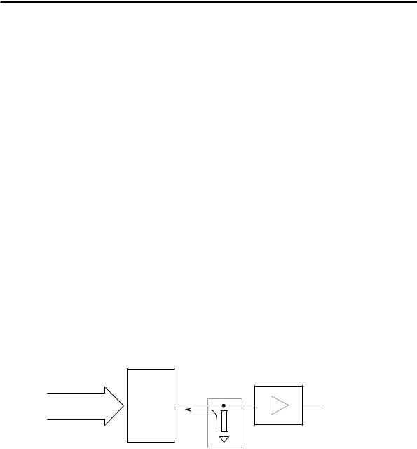
The DAC used in the interface board is the DAC0800, an 8-bit device providing a programmable output current. We use this programmable output current with a current-to-voltage circuit to generate a voltage output. Figure 6-8 shows a block diagram of the DAC0800 circuit used on the interface board.
The DAC0800 produces an output current, where the current flowing through its output pin actually flows into the DAC (sink current). To generate an analog voltage, we need to use a current-to-voltage converter, in this case a single resistor, R, one end connected to the DAC output pin and the other end to a reference voltage, 0V, as shown in Figure 6-8. When current i flows through the resistor, a voltage V ( V = i x R) is generated across the resistor. Knowing that current flows from a more positive voltage to a less positive voltage, the voltage at the end of the resistor, R, which connects to the DAC output, will be equal to 0V + - V = -V. With a current i equal to zero, the output voltage generated across resistor R will be 0V.
8-bit Logic
(8 lines)
8 Digital Inputs |
Current Output (sinking) |
DAC0800
Vout
i
R
Voltage Buffer
& Inverter
Current to
Voltage
Converter
Figure 6-8 Block diagram - Interface board DAC0800 circuit.
So we have a programmable output voltage ranging from 0V to - V, where the actual value of V for a given digital input will be dependent on the resistance value of resistor R. A DAC output range that always remains on the same side of