

2.3. DIGITAL I/O |
33 |
2.3 Digital I/O
Digital I/O, or, to be more general, the ability to directly monitor and control hardware, is the main characteristic of microcontrollers. As a consequence, practically all microcontrollers have at least 1-2 digital I/O pins that can be directly connected to hardware (within the electrical limits of the controller). In general, you can find 8-32 pins on most controllers, and some even have a lot more than that (like Motorola’s HCS12 with over 90 I/O pins).
I/O pins are generally grouped into ports of 8 pins, which can be accessed with a single byte access. Pins can either be input only, output only, or —most commonly,— bidirectional, that is, capable of both input and output. Apart from their digital I/O capabilities, most pins have one or more alternate functions to save pins and keep the chip small. All other modules of the controller which require I/O pins, like the analog module or the timer, use in fact alternate functions of the digital I/O pins. The application programmer can select which function should be used for the pin by enabling the functionality within the appropriate module. Of course, if a pin is used for the analog module, then it is lost for digital I/O and vice versa, so the hardware designer must choose carefully which pins to use for which functions.
In this section, we will concentrate on the digital I/O capability of pins. Later sections will cover the alternate functions. First, let us explain what we mean by “digital”: When we read the voltage level of a pin with a voltmeter (with respect to GND), we will see an analog voltage. However, the microcontroller digitizes this voltage by mapping it to one of two states, logical 0 or logical 1. So when we talk about digital I/O, we mean that the value of the pin, from the controller’s perspective, is either 1 or 0. Note that in positive-logic, 1 corresponds to the “high” state (the more positive resp. less negative state) of the line, whereas 0 corresponds to the “low” state (the less positive resp. more negative state). In negative-logic, 1 corresponds to “low” and 0 to “high”. Microcontrollers generally use positive-logic.
As far as digital I/O is concerned, three registers control the behavior of the pins:
Data Direction Register (DDR): Each bidirectional port has its own DDR, which contains one bit for each pin of the port. The functionality of a pin (input or output) is determined by clearing or setting its bit in the DDR. Different pins of a port may be configured differently, so it is perfectly okay to have three pins configured to output and use the other five as inputs. After a reset, the DDR bits are generally initialized to input. Reading the register returns its value.
Port Register (PORT): This register is used to control the voltage level of output pins. Assuming a pin has been configured to output, then if its bit in the PORT register is set, the pin will be high; if the bit is cleared, the pin will be low. To avoid overwriting the other bits in the port when setting a particular bit, it is generally best to use the controller’s bit operations. Otherwise, you must use a read-modify-write access and hence must ensure that this access is not interrupted.
For output pins, reading the register returns the value you have written. For input pins, the functionality depends on the controller. Some controllers allow you to read the state of input pins through the port register. Other controllers, e.g. the ATmega16, use the port bits for other purposes if the corresponding pins are set to input, so here you will read back the value you have written to the register.
Port Input Register (PIN): The PIN register is generally read-only and contains the current state (high or low) of all pins, whether they are configured as output or as input. It is used to read the state of input pins, but it can also be used to read the state of output pins to verify that the output was taken over correctly. A write to this register generally has no effect.

34 |
CHAPTER 2. MICROCONTROLLER COMPONENTS |
Read-Modify-Write Access
A read-modify-write access is used to modify some bits within a byte without changing the others in situations where bit operations are not an option. The idea is to (1) read the whole byte, (2) change the bits you are interested in while keeping the states of the other bits, and (3) write the resulting value back. Hence, the whole operation consists of at least three instructions, possibly even more.
Within a single-taskinga microprocessor that just accesses memory locations, this is not a problem. However, in a multi-tasking system, or in a hardware-based system where register contents may be modified by the hardware, read-modify-write operations must be used with care. First of all, there is the question of how many sources can modify the byte in question. Obviously, your task code can modify it. If there is another source that can modify (some other bits of) the byte “concurrently”, e.g. in a multi-tasking system, then you can get a write conflict because Task1 reads and modifies the value, but gets interrupted by Task2 before it can write back the value. Task2 also reads the value, modifies it, and writes back its result. After that, Task1 gets back the CPU and writes back its own results, thus overwriting the modifications of Task2! The same problem can occur with a task and an ISR. In such a case, you must make sure that the read-modify-write operation is atomic and cannot be interrupted.
If the byte is an I/O register, that is, a register which controls and/or can be modified by hardware, the problem is even more urgent because now the hardware may modify bits anytime. There is also the problem that registers may be used for two things at once, like an I/O register that can function as a status register during read accesses and as a control register for write accesses. In such a case, writing back the value read from the register would most likely have undesired effects. Therefore, you must be especially careful when using I/O registers within read-modify-write operations.
aWe have not introduced the notion of tasks up to now, since we concentrate on small systems which will most likely not run an operating system. However, this discussion can be generalized to operating systems as well, so we use the term “task” here and trust that you know what we mean.
Let us stress again that each bit in these registers is associated with one pin. If you want to change the settings for one pin only, you must do so without changing the settings of the other bits in the register. The best way to do this, if it is supported by your controller, is to use bit operations. If you have to use read-modify-write operations on the whole register, at least make certain that the register’s contents will not change during the operation and that it is okay to write back to the register what you have read from it.
2.3.1Digital Input
The digital input functionality is used whenever the monitored signal should be interpreted digitally, that is, when it only changes between the two states “high” (corresponding to logic 1) and “low” (corresponding to 0). Whether a given signal should be interpreted as high or low depends on its voltage level, which must conform to the controller’s specifications, which in turn depend on the operating voltage of the controller. For example, the operating voltage VCC of the ATmega16 must be within the interval [4.5, 5.5] V, its input low voltage must be within [-0.5, 0.2VCC] V, and its input
2.3. DIGITAL I/O |
35 |
high voltage must be within [0.6VCC, VCC+0.5] V. This leaves the interval (0.2VCC, 0.6VCC) within which the signal is said to be undefined.
Digital Sampling
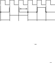
Since the digital signal is just a voltage value, the question arises how this voltage value is transformed into a binary value within a register. As a first solution, we could simply use latches for the PIN register and latch the current state of the pin into the register. If the latch is triggered by the system clock, it will store the current state at the beginning of every cycle. Naturally, since we can only sample with the granularity of the system clock, this means that we may recognize a state change only belatedly. We may even miss impulses altogether if they are shorter than a clock cycle, see Figure 2.9.
clock
 w.c. delay
signal
PIN
Figure 2.9: Sampling an input signal once every clock cycle.
The delay introduced by the sampling granularity is dlatch = (0, 1] clock cycles. Note that zero is left out here, since it is not certain what happens when a signal changes at the same time as the sampling clock edge. It may get sampled, or it may not get sampled. It is therefore prudent to leave zero out of the interval. With the same reasoning, impulses should be longer than a clock cycle to be recognized with certainty. In the remaining text, we will use din = (dminin , dmaxin ] to denote the input delay interval, where dminin forms the lower bound on the input delay, and dmaxin denotes its upper bound.
Although this sampling technique looks quite useful and forms the basis of the controller’s input circuitry, it is unsuited to deal with a situation often encountered in real systems: What happens if the signal is slow to change? After all, the signal is generated by the hardware, which may behave unpredictably, so we do not have any guarantee that signal changes will be fast and may run into the problem that the signal is undefined when we try to latch. In this case, our simple solution runs head-long into the problem of meta-stability: A latch that gets an undefined voltage level as input has a certain probability p to enter and remain in a meta-stable state, in which it may output either high, or low, or an undefined value, or oscillate. Obviously, the last two options are disastrous for the controller and hence for the application and must be avoided, especially in safety-critical systems. To decrease the probability of such an occurence, the digital input circuitry of a controller generally first uses a Schmitt-trigger to get well-defined edges and filter out fluctuations in the input voltage. This restricts the problem to the short periods during which the Schmitt-trigger switches its output.
To reduce the probability of meta-stability even further, one or more additional latches may be set in series between the Schmitt-trigger and the PIN register latch. Such a construct is called a synchronizer. Figure 2.11 shows a block diagram of the resulting circuitry. Each additional synchronizer latch has the probability p to enter a meta-stable state if presented with an undefined input, so the whole chain of k latches including the PIN latch has probability pk 1 to pass on the meta-stable
36 |
CHAPTER 2. MICROCONTROLLER COMPONENTS |
Schmitt-trigger
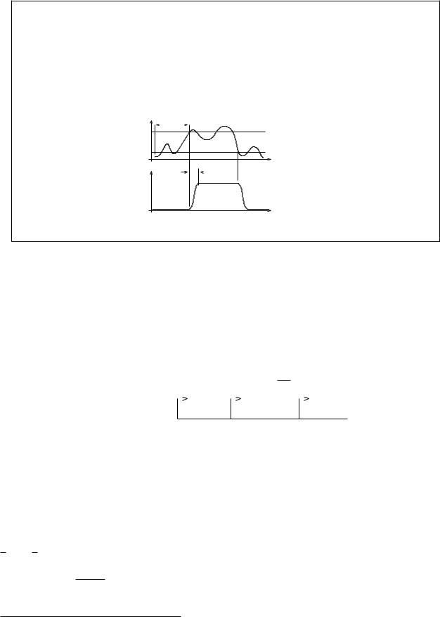
Schmitt-triggers are components that can be used to “digitize” analog input signals. To do so, the Schmitt-trigger has two threshold voltages Vlo and Vhi, Vlo <Vhi, and changes its output from logical 0 to logical 1 only if the input signal rises above Vhi. To make the Schmitt-trigger change from 1 to 0, however, the signal must fall below Vlo. As a result, the Schmitt-trigger does not forward small voltage fluctuations, and its output always has short and well-defined rising and falling times regardless of the input signal, see Figure 2.10.
V unbounded |
|
Vhi |
input signal |
|
|
Vlo |
t |
|
|
V |
bounded |
Schmitt−trigger |
output |
t |
Figure 2.10: Input and Output of a Schmitt-trigger.
state all to way to the controller. In practice, one synchronizer latch generally suffices to bring the probability down to an acceptable level (but it will never be zero, no matter how many latches are used).
|
|
Schmitt− |
Synchr. |
Synchr. |
PIN |
||||||||||||||||||
input |
|
trigger |
Latch |
Latch |
Latch |
||||||||||||||||||
|
|
|
|
|
|
|
|
|
|
|
|
|
|
|
|
|
|
||||||
|
|
|
|
|
|
|
D Q |
|
|
D Q |
|
|
|
|
D Q |
||||||||
signal |
|
|
|
|
|
|
|
|
|
|
|
|
|
||||||||||
|
|
|
|
|
|
|
|
|
|
|
|
|
|
|
|
|
|
|
|
|
|||
|
|
|
|
|
|
|
|
|
|
Q |
|
|
|
|
Q |
|
|
|
|
|
|
Q |
|
|
|
|
|
|
|
|
|
|
|||||||||||||||
|
|
|
|
|
|
|
|
|
|
|
|
|
|
|
|
|
|
|
|
|
|||
system clock
Figure 2.11: Block diagram of the basic input circuitry of a controller.
You may already have spotted the disadvantage of the synchronizer stage: It prolongs the time until a signal change is passed on to the controller by a constant dsync, which is simply the number of cycles it takes to pass a latched value from the first synchronizer latch to the PIN latch. Hence, din = dlatch + dsync. The ATmega16 controller, for instance, uses one synchronizer latch which is triggered by the falling edge of the system clock (whereas everything else is triggered by the rising edge). Hence, the synchronizer stage adds a delay of half a clock cycle, and the delay bounds for the ATmega16 become dminin = 0.5 and dmaxin = 1.5 clock cycles3.
3Note that we ignore the propagation delays of the Schmitt-trigger and the PIN latch here, which add an additional couple of nanoseconds (about 20-30).
2.3. DIGITAL I/O |
37 |
Noise Cancellation
Although the PIN register of the controller should normally follow the state of the input pin as closely as possible, this is quite undesired if the signal is noisy. Here, electromagnetic interference from the environment produces short voltage spikes on the line, and these voltage changes should normally not be taken over by the controller, where they could produce erroneous reactions, especially in conjunction with interrupts.
Therefore, some controllers provide noise cancellation. If enabled, the controller samples the pin not just once but several times, e.g. k times, and only takes over a new value if all k samples were equal. Obviously, this adds another constant dncanc = k − 1 cycles to the overall input delay, so the bounds on the delay become
din = dlatch + dsync + dncanc |
(2.1) |
clock cycles.
Pull Resistors
Many controllers integrate pull resistors into their input circuitry. Most of the time, they provide pull-up resistors, some controllers also offer pull-down resistors (e.g. the HCS12). The task of the pull resistor is to connect the input pin to a defined voltage if it is not driven by the external hardware. Pull resistors are controlled via a register, where they can be enabled or disabled for each pin independently. The ATmega16, for example, uses the PORT register bits of input pins for controlling their pull resistors. Other controllers provide dedicated registers for this purpose.
It can occur quite frequently that an input pin is not driven by hardware all the time, most notably when using simple mechanical switches, like DIP switches or buttons. Here, the input pin is connected to a defined value as long as the switch is closed, but left floating (that is, unconnected and at an undefined voltage level) whenever the switch is open. Since floating pins are A Bad Thing (they are very prone to noise!), a pull resistor must be used to set the pin to a defined level while the switch is open, see Figure 2.12 for an example.
Controller−Input. |
1 2 |
Figure 2.12: Attaching a switch to an input pin with activated pull-up resistor.
In the figure, we connected the switch to an input with activated pull-up, also called an open-drain input. While the switch is open, the input pin is connected to VCC and the controller will read a 1. Closing the switch connects the pin to ground, and the controller will read 0.
There is another interesting thing to note in Figure 2.12: Due to the pull-up resistor, whenever the switch is closed, current flows from the controller via the input pin to the external ground. Without a pull resistor, there would not be any notable current flow from or to the controller pin, since the