

40 |
CHAPTER 2. MICROCONTROLLER COMPONENTS |
2.4 Analog I/O
In the previous section, we have covered digital I/O. There, analog signals were mapped to two discrete values 0 and 1. Although this is already very useful, there are situations in which the actual voltage of the line transports information, e.g. when using a photo transistor as light sensor: The voltage drop it produces at its output is directly proportional to the amount of light falling on the transistor, and to adequately evaluate the sensor output, the microcontroller must deal with the analog value. On the other hand, the microcontroller is inherently digital, so we need appropriate ways of converting analog signals into the digital world and back again. This problem is addressed by the analog module of the microcontroller.
In the following text, we will give an overview on analog interfacing techniques and problems. A thorough treatment of this subject can be found e.g. in [Hoe94] or in [Bal01].
2.4.1Digital/Analog Conversion
Since digital-to-analog conversion is a prerequisite for some analog-to-digital converters, we begin with analog output. This means that we have an r-bit digital value B = (br−1 · · · b0)2, r ≥ 1, in the range [0, 2r − 1] and want to generate a proportional analog value Vo.
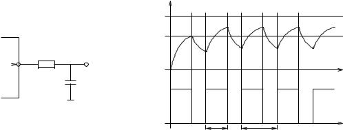
Yet, as powerful as they are when it comes to analog input, microcontrollers often have little or no analog output capabilities. So if the application requires a d/a converter, most of the time it has to be fitted externally. Fortunately, it is fairly easy to construct a simple and cheap 1-bit d/a converter by using a PWM (pulse-width modulation) output, see Section 2.6, in conjunction with an RC low-pass filter. The idea here is to generate a PWM signal whose high time to period ratio is proportional to the digital value B. The PWM signal is smoothened by the RC filter, resulting in an (average) analog voltage that is proportional to the high time to period ratio of the PWM signal and hence to B, see Figure 2.13. Of course, the resulting analog signal is delayed by the filter before it stabilizes, and it does not show very good quality, as it will oscillate around the desired output voltage. Still, it will be sufficient for some applications like motor control.
|
|
Vo |
|
|
Vmax |
MCU |
|
|
PWM |
R |
|
Vo |
|
|
|
t |
|
|
C |
PWM |
|
|
|
|
|
t |
high time |
period |
(a) |
(b) |
Figure 2.13: Digital-to-analog conversion using a PWM signal and an RC low-pass filter; (a) circuit,
(b) output voltage in reaction to PWM signal.
2.4. ANALOG I/O |
41 |
The oscillation depends on R and C as well as on your choice of period; Figure 2.13 greatly exaggerates the effect. To reduce the amount of oscillation, either make R and C larger (at the cost of a longer stabilization time) or use a shorter period.
Disadvantages of using PWM are that you require a dedicated timer to generate the PWM signal and that you need to wait for a few periods until the output signal stabilizes. As an advantage, the d/a converter only uses up one single output pin.
A different way to achieve d/a conversion is to use a binary-weighted resistor circuit, see Figure 2.14. Here, we have an r-bit input which is converted into the appropriate analog output. To this aim, each bit of the binary input switches its path between Vref and GND. The output voltage of the circuit (for no output load) is given by
|
r |
1 |
|
|
|
Vo = Vref · |
Xi |
|
|
(2.2) |
|
2i br−i , |
|||||
=1 |
|||||
where (br−1 · · · b0)2 is the digital value to be converted.
R/2r−1
b r−1 . Vo
..
b 1 |
R/2 |
|
R |
||
b 0 |
||
|
R
Figure 2.14: Digital-to-analog conversion based on a binary-weighted resistor circuit.
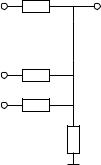
The main disadvantage of the binary-weighted resistor circuit is that it requires many different resistor types with have to be high precision to keep the ratio correct. This is hard to achieve. As an alternative, an R-2R resistor ladder can be employed, see Figure 2.15.
This type of DAC has the advantage that it only requires two types of resistors, R and 2R. The output voltage of the ladder circuit is again given by Equation 2.2.
2.4.2Analog Comparator
The simplest way to deal with analog inputs in a microcontroller is to compare them to each other or to a known reference voltage. For example, the phototransistor we mentioned previously could be used to implement a twilight switch, turning on a light whenever its output voltage indicates that the ambient light level is below some threshold. For such purposes, some microcontrollers which
42 |
CHAPTER 2. MICROCONTROLLER COMPONENTS |
||||||||
b r−1 |
|
|
2R |
|
|
|
|
|
V |
|
|
|
|
|
|
|
|
||
|
|
|
|
|
|
|
|
||
|
|
. |
|
|
|
R |
o |
||
|
|
|
|
|
|
||||
|
. |
|
|
|
|
|
|
||
|
|
|
|
|
|
|
|||
|
. |
|
|
|
|
|
|
||
|
|
|
2R |
|
|
|
R |
|
|
b 1 |
|
|
|
|
|
R |
|
||
|
|
|
|
|
|
|
|||
|
|
|
|
|
|
|
|||
|
|
2R |
|
|
|
|
|||
|
|
|
|
|
|
|
|||
b 0 |
|
|
|
|
|
2R |
|
||
|
|
|
|
|
|
||||
|
|
|
|
|
|
|
|||
|
|
|
|
|
|
|
|||
|
|
|
|
|
|
|
|||
|
|
|
|
|
|
|
|
||
|
|
|
|
|
|
|
|
|
|
|
|
|
|
|
|
|
|
|
|
Figure 2.15: Digital-to-analog conversion based on an R-2R resistor ladder.
V1  +
+
 O
O
V2  −
−
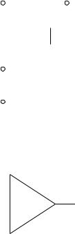
Figure 2.16: Analog comparator.
feature an analog module include an analog comparator. Comparators are a bit like digital inputs, but without a Schmitt-trigger and with a configurable threshold. The analog comparator has two analog inputs and one (digital) output, see Figure 2.16. It simply compares the two input voltages V1 and V2 and sets its output to 1 if V1 > V2. For V1 ≤ V2, the output is set to 0.
The input voltages are either both from external analog signals, or one of them is an external signal and the other is an internally generated reference voltage. The output of the comparator can be read from a status register of the analog module. Furthermore, controllers generally allow an interrupt to be raised when the output changes (rising edge, falling edge, any edge). The ATmega16 also allows the comparator to trigger an input capture (see Section 2.6.2).
Like digital inputs, comparator outputs suffer from meta-stability. If the two compared voltages are close to each other and/or fluctuate, the comparator output may also toggle repeatedly, which may be undesired when using interrupts.
2.4.3Analog/Digital Conversion
If the voltage value is important, for example if we want to use our photo transistor to determine and display the actual brightness, a simple comparator is not sufficient. Instead, we need a way to represent the analog value in digital form. For this purpose, many microcontrollers include an analog-to-digital converter (ADC) which converts an analog input value to a binary value.
Operating Principle
2.4. ANALOG I/O |
|
|
code |
|
|
111 |
|
|
110 |
|
|
101 |
|
|
100 |
|
|
011 |
|
|
010 |
|
|
001 |
|
|
000 |
Vref /8 |
Vin |
|
Vref |
|
|
= 1 lsb |
(a) |
|
|
|
43
code |
|
|
Vin |
|
|
|
|
Vref |
|
111 |
|
|
7 lsb |
|
110 |
|
|
6 lsb |
|
101 |
|
(2) |
5 lsb |
|
100 |
|
4 lsb |
|
|
|
|
|
||
011 |
|
|
3 lsb |
|
010 |
(1) |
|
2 lsb |
|
001 |
|
(1) |
1 lsbVref /16 |
|
|
|
|||
000 |
2τs |
3τs 4τs |
t |
=0.5 lsb |
τs |
|
|
||
|
|
(b) |
|
|
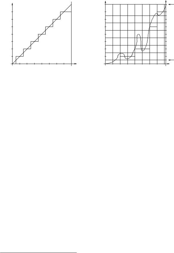
Figure 2.17: Basic idea of analog to digital conversion (r = 3, GND=0). (a) Mapping from analog voltage to digital code words, (b) example input and conversion inaccuracies.
Figure 2.17 (a) shows the basic principle of analog-to-digital conversion. The analog input voltage range [GND, Vref ] is parted into 2r classes, where r is the number of bits used to represent the digital value. Each class corresponds to a digital code word from 0 to 2r − 1. The analog value is mapped to the representative of the class, in our case the midpoint, by the transfer function. We call r the resolution, but you will also find the term word width in the literature. Typical values for r are 8 or 10 bits, but you may also encounter 12 bit and more. The lsb of the digital value represents the smallest voltage difference Vref /2r that can be distinguished reliably. We call this value the granularity of the a/d converter, but you will often find the term resolution in the literature6. The class width of most classes corresponds to 1 lsb, with the exceptions of the first class (0.5 lsb) and the last class (1.5 lsb). This asymmetry stems from the requirement that the representative of the code word 0 should correspond to 0 V, so the first class has only half the width of the other classes, whereas the representative of the code word 2r − 1 should be Vref − 1 lsb to allow easy and compatible expansion to more bits. To avoid the asymmetry, we could for example use the lower bound of the class as its representative. But in this case, the worst case error made by digitization would be +1 lsb. If we use the midpoint, it is only ± 0.5 lsb.
As you can see in Figure 2.17 (b), the conversion introduces some inaccuracies into the microcontroller’s view of the analog value. First of all, the mapping of the analog value into classes results in information loss in the value domain. Fluctuations of the analog value within a class go unnoticed, e.g. both points (1) in the figure are mapped to the same code word 001. Naturally, this situation can be improved by reducing the granularity. One way to achieve this is to make r larger, at the cost of a larger word width. Alternatively, the granularity can be improved by lowering Vref , at the cost of a smaller input interval.
Secondly, the conversion time, which is the time from the start of a conversion until the result of this conversion is available, is non-zero. In consequence, we get a certain minimum sampling period
6Actually, “resolution” is used very frequently, whereas “granularity” is not a term generally used, it is more common in clock synchronization applications. But to avoid confusion with the resolution in the sense of word width, we decided to employ the term granularity here as well.
44 |
CHAPTER 2. MICROCONTROLLER COMPONENTS |
τs between two successive conversions, resulting in an information loss in the time domain7. Changes of the value between two conversions are lost, as you can see at point (2) in the figure. The upper bound on the maximum input frequency fmax that can be sampled and reconstructed by an ADC is given by Shannon’s sampling theorem (Nyquist criterion):
fmax < |
fs |
= |
1 |
(2.3) |
|
2τs |
|||
2 |
|
|
||
The theorem states that the maximum input signal frequency fmax must be smaller than half the sampling frequency fs. Obviously, this implies that for high input frequencies the minimum sampling period τs, which depends on the conversion technique used, should be small.
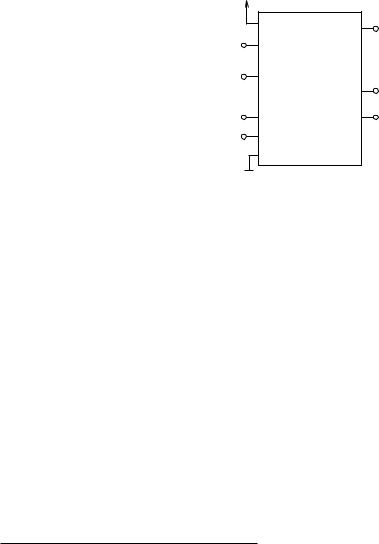
Figure 2.18 shows a simple a/d converter as a black box. The AVCC and GND pins provide the power supply for the converter. Vref provides the ADC with the maximum voltage used for conversion, and on Vin the measurand is connected to the converter. An enable input and a trigger input to start a new conversion complete the input part of our simple ADC. On the output side, we have the converted value and a signal line which indicates a completed conversion.
AVCC |
b r−1 |
|
|
||
VREF |
. |
|
|
. |
|
Vin |
. |
|
b 0 |
||
|
||
SC |
CC |
|
EN |
|
|
GND |
|
Figure 2.18: An ADC as a black box.
In the figure, the maximum voltage Vref , the reference voltage used for defining the conversion interval, is provided on an external pin. However, some controllers also offer an internal reference voltage. The ATmega16, for example, allows the user to choose between an internal 2.56 V reference voltage, the (external) analog power supply voltage AVCC, or an external reference voltage. If the analog input signal is greater than Vref , it is mapped to 2r − 1. More sophisticated a/d converters may indicate such an overflow in a dedicated overflow bit. Likewise, a signal smaller than GND is mapped to the code 0.
Fluctuations of the input signal during a conversion can deteriorate the quality of the result, so in order to keep the input signal stable during conversion, a sample/hold stage is used, see Figure 2.19. At the start of the conversion, the capacitor is charged from the input signal. After a fixed time, it is disconnected from the input signal and is used as input to the ADC itself, ensuring that the voltage remains constant during conversion.
7Note that τs is not necessarily equal to the conversion time: Some converters allow to pipeline conversions, thus achieving a τs that is shorter than the conversion time of a single value.
2.4. ANALOG I/O |
45 |
||||||||||||
|
|
|
|
R |
|
|
|
|
|
buffer |
|||
Vin |
|
|
|
|
|
|
|
|
|
|
to ADC |
||
|
|
|
|
|
|
|
|
|
|
|
|
|
|
|
|
|
|
|
|
|
|
C |
|||||
|
|
|
|
|
|
||||||||
|
|
|
|
|
|
|
|
|
|
||||
|
|
|
|
|
|
|
|
|
|
|
|
|
|
Figure 2.19: Sample/hold stage of an a/d converter.
Conversion Techniques
There are several different techniques for analog-to-digital conversion. The simplest one is the flash converter, see Figure 2.20.
Vin |
|
|
|
+ |
|
|
msb |
|
|
|
|
|
|
|
|
|
|
||||||
|
Vref,2r −1 |
|
− |
|
|
|
|||||
|
|
|
|
|
|
|
|
|
|||
|
|
(2r −1.5 lsb) |
. |
|
|
priority |
|
b |
|
||
|
|
|
|
||||||||
|
|
|
|
. |
|
|
encoder |
|
|
|
|
|
|
|
|
. |
|
|
|
. |
|
r−1 |
|
|
|
|
|
|
|
||||||
|
|
|
|
+ |
|
|
|
. |
|
|
|
|
|
|
|
|
|
||||||
|
|
Vref,2 |
|
− |
|
|
. |
|
|
||
|
|
|
|
|
|
||||||
|
|
|
|
|
|
|
|
|
|||
|
|
(1.5 lsb) |
+ |
|
|
|
|
|
b 0 |
||
|
|
|
|
|
|
|
|||||
|
|
|
|
|
|
|
|
|
|
|
|
|
|
Vref,1 |
|
− |
|
|
|
|
|
|
|
|
|
|
|
|
|
|
|
|
|||
|
|
|
|
|
|
|
|
|
|||
|
|
(0.5 lsb) |
1 |
|
|
lsb |
|
|
|
|
|
|
|
|
|
|
|
|
|
|
|||
|
|
|
|
|
|
|
|
|
|
||
|
|
|
|
|
|
|
|
|
|
|
|
Figure 2.20: Operating principle of a flash converter.
The idea is very simple: The input voltage Vin is compared to several reference voltages Vref,i,
where |
|
|
Vref · (2i − 1) |
|
|
|
|
|
|
|
|
|
V |
ref,i |
= |
, 1 |
≤ |
i |
≤ |
2r |
− |
1. |
(2.4) |
||
2r+1 |
||||||||||||
|
|
|
|
|
|
|
If the input voltage is higher than a particular reference voltage, then its comparator will output 1. All comparator outputs are connected to a priority encoder which will output the binary number that corresponds to the most significant bit that is set in the input value. The lsb of the encoder is connected to 1, so if none of the comparators is active, the encoder will output the code word 0.
With the reference voltages of Equation 2.4, we again get a class width of 0.5 lsb for code 0, a width of 1.5 lsb for code 2r − 2, and widths of 1 lsb for all other classes.
The major advantage of the flash converter, which lends it its name, is its speed: the conversion is done in one step, all possible classes to which the input voltage may correspond are checked simultaneously. So its time complexity is O(1). However, the fast conversion is bought with enormous hardware complexity: 2r −1 comparators are required, and adding just one more bit to the code word doubles the hardware requirements. Therefore, flash converters are rather expensive.
46 |
CHAPTER 2. MICROCONTROLLER COMPONENTS |
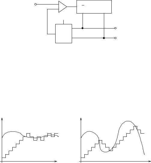
A completely different concept is implemented in the tracking converter, see Figure 2.21.
Vin |
+ |
U/D Counter |
|
|
− |
. . . |
|
|
Vref |
|
|
|
. |
. |
b r−1 |
|
DAC . |
. |
|
|
. |
. |
b |
|
|
|
0 |
Figure 2.21: Operating principle of a tracking converter.
This converter is interesting in that it requires a d/a converter to achieve a/d conversion. The principle is again very simple: The heart of the tracking converter is a counter which holds the current digital estimate of the input voltage. The counter value is converted to an analog value by the DAC and compared to the input voltage. If the input voltage is greater than the current counter value, then the counter is incremented, otherwise it is decremented.
Vin
t |
(a) |
Vin
t |
(b) |
Figure 2.22: A tracking converter in action.
As you can see in Figure 2.22 (a), the tracking converter requires a long time until it catches the signal, but once it has found the signal, its conversion time is pretty fast. Unfortunately, this is only true for a slowly changing signal. If the signal changes too fast, as depicted in part (b) of the figure, then the converter again spends most of its time tracking the signal. Only the points where the count direction changes are correct conversion values.
Since the worst case time complexity of the tracking converter is O(2r), it is too slow for many applications.
By slightly changing the operating principle of the tracking converter, we get the successive approximation converter shown in Figure 2.23.
2.4. ANALOG I/O |
|
|
|
|
|
|
|
|
|
|
|
|
47 |
|
Vin |
|
|
|
+ |
|
|
|
|
|
|
|
|
|
|
|
|
|
|
|
|
K SAR |
|
|
||||||
|
|
|
|
|
||||||||||
|
|
|
− |
|
|
|||||||||
|
|
|
|
|
|
. . . |
|
|
|
|
||||
|
|
|
|
Vref |
|
|
|
|
|
|
||||
|
|
|
|
|
|
|
|
|
||||||
|
|
|
|
|
|
|
. |
|
|
|
|
. |
|
b r−1 |
|
|
|
|
DAC |
|
|
|
|||||||
|
|
|
|
|
||||||||||
|
|
|
|
. |
|
|
. |
|
|
|||||
|
|
|
|
|
. |
|
|
. |
|
b |
||||
|
|
|
|
|
|
|
|
|||||||
|
|
|
|
|
|
|
|
|
|
|
|
|||
|
|
|
|
|
|
|
|
|
|
|
|
|
0 |
|
Figure 2.23: Operating principle of a successive approximation converter.
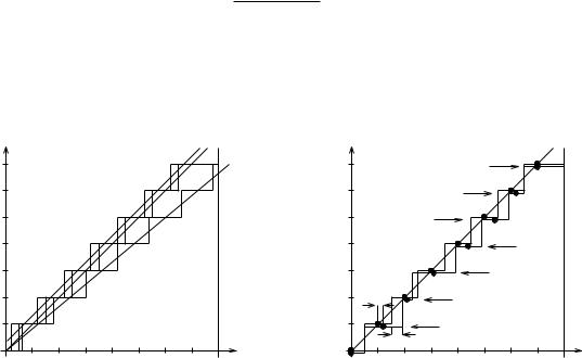
As you can see, the only difference is that the counter was exchanged for a successive approximation register (SAR). The SAR implements a binary search instead of simply counting up or down: When a conversion is started, the msb in the SAR (b2r−1) is set and the resulting analog value is compared to the input voltage. If the input is greater than that voltage, b2r−1 is kept, otherwise it is cleared. Then the next bit b2r−2 is set, and so on, until the last bit. After r comparisons, the value in the SAR corresponds to the input voltage. Figure 2.24 demonstrates the operation.
|
|
|
|
|
|
|
|
|
|
|
|
|
|
|
|
|
|
000 |
|
|
|
|
|
|
|
|
|
|
|
reset SAR, start conversion |
|||||||||||||||||||||
|
|
|
|
|
|
|
|
|
|
|
|
|
|
|
|
|
|
|
|
|
|
|
|
|
|
|
|
|
|
|
|
|
|
|
|
|
|
|
|
|
|
|
|
|
|||||||
|
|
|
|
|
|
|
|
|
|
|
|
|
|
|
|
|
|
|
|
|
|
|
|
|
|
|
|
|
|
|
|
|
|
|
|
|
|
|
|
|
|
|
|
|
|
|
|
|
|
|
|
|
|
|
|
|
|
|
|
|
|
|
|
|
|
|
|
|
|
|
|
|
|
|
100 |
|
|
|
|
|
|
|
|
|
|
|
|
|
|
|
|
|
|
|
|
test bit r−1=2 |
|||||||
|
|
|
|
|
|
|
|
|
|
|
|
|
|
|
|
|
|
|
|
|
|
K=1 |
|
K=0 |
|
|
|
|
|
|
|
|
|
|
|
|
|
|
|
|
|
|
|
|
|
|
|||||
|
|
|
|
|
|
|
|
|
|
|
|
|
|
|
|
|
|
|
|
|
|
|
|
|
|
|
|
|
|
|
|
|
|
|
|
|
|
|
|
|
|
|
|
|
|
|
|
|
|
|
|
|
|
|
|
|
|
|
|
|
|
|
|
|
|
|
|
|
|
|
|
|
|
|
|
|
|
|
|
|
|
|
|
|
|
|
|
|
|
|
|
|
|
|
|
|
|
|
|
|
|
|
|
|
|
|
|
|
|
|
|
|
|
|
110 |
|
|
|
|
|
|
|
|
|
|
|
|
|
|
|
|
|
|
010 |
|
|
|
|
|
|
|
|
|
|
test bit 1 |
||||||||||
|
|
|
|
|
|
|
|
|
K=1 |
|
|
K=0 |
|
|
|
|
|
|
|
|
|
|
|
|
|
|
|
|
|
|
|
K=1 |
|
K=0 |
|
|
|
|
|||||||||||||
|
|
|
|
|
|
|
|
|
|
|
|
|
|
|
|
|
|
|
|
|
|
|
|
|
|
|
|
|
|
|
|
|
|
|
|
|
|
|
|
|
|
|
|
|
|
|
|
|
|
test bit 0 |
|
|
|
|
|
|
|
|
|
|
|
|
|
|
|
|
|
|
|
|
|
|
|
|
|
|
|
|
|
|
|
|
|
|
|
|
|
|
|
|
|
|
|
|
|
|
|
|
|
|
|
||
|
|
|
111 |
|
|
|
|
|
|
|
|
|
101 |
|
|
|
|
|
|
|
|
|
011 |
|
|
|
|
|
|
|
001 |
|
|
||||||||||||||||||
|
|
|
|
|
|
|
|
|
|
|
|
|
|
|
|
|
|
|
|
|
|
|
|
|
|
|
|
|
|
|
|
|
|
|
|
|
|
|
|
|
|
|
|
|
|
|
|
|
|||
K=1 |
|
|
|
|
K=0 |
|
|
|
K=1 |
|
|
|
K=0 |
|
K=1 |
|
|
|
|
K=0 |
|
|
K=1 |
|
K=0 |
|
|||||||||||||||||||||||||
|
|
|
|
|
|
|
|
|
|
|
|
|
|
|
|
|
|
|
|
|
|
|
|
|
|
|
|
|
|
|
|
|
|
|
|
|
|
|
|
|
|
|
|
|
|
|
|
|
|
|
conversion |
111 |
|
|
|
|
110 |
|
|
|
101 |
|
|
|
100 |
|
|
|
011 |
|
|
|
|
010 |
|
|
|
001 |
|
|
|
000 |
|||||||||||||||||||||
|
|
|
|
|
|
|
|
|
|
|
|
|
|
|
|
|
|
|
|
|
|
|
finished |
||||||||||||||||||||||||||||
|
|
|
|
|
|
|
|
|
|
|
|
|
|
|
|
|
|
|
|
|
|
|
|
|
|
|
|
|
|
|
|
|
|
|
|
|
|
|
|
|
|
|
|
|
|
|
|
|
|
|
|
|
|
|
|
|
|
|
|
|
|
|
|
|
|
|
|
|
|
|
|
|
|
|
|
|
|
|
|
|
|
|
|
|
|
|
|
|
|
|
|
|
|
|
|
|
|
|
|
|
|
|
|
Figure 2.24: A successive approximation register in action (r=3).
The successive approximation converter with its linear time complexity of O(r) is a good compromise between the speed of the flash converter and the simplicity of the tracking converter. Another advantage over the tracking converter is that its conversion time does not depend on the input voltage and is in fact constant. To avoid errors during conversion due to a changing input signal, a sample/hold stage is required.
Successive approximation converters are commonly used in microcontrollers.
48 |
CHAPTER 2. MICROCONTROLLER COMPONENTS |
Errors
As we have already mentioned at the beginning of the chapter, the digital representation of an analog value is not exact. The output code C(Vin), GND ≤ Vin ≤ Vref , of the ideal transfer function is
C(Vin) = min |
Vin |
− |
GND |
· 2r + 0.5 , 2r − 1 , |
(2.5) |
|
Vref |
GND |
|||||
− |
||||||
|
|
|
|
|
so at the very least, its accuracy will be limited to ± 0.5 lsb due to the quantization error. However, the actual accuracy, which is the difference of the actual transfer function from the ideal one, may be even worse. Figure 2.25 depicts the errors that an a/d converter can exhibit.
code |
|
|
|
111 |
|
(a) |
ideal |
|
|
||
110 |
|
|
|
101 |
|
|
(b) |
100 |
|
|
|
011 |
|
|
|
010 |
|
|
|
001 |
|
|
|
000 |
Vref /8 |
|
Vin |
|
|
Vref |
|
code |
|
|
|
111 |
|
D=0 lsb, I=0 lsb |
ideal |
|
|
(c) |
|
|
D=−0.4 lsb, I=0.2 lsb |
||
110 |
|
||
|
|
|
|
101 |
D=0, I=+0.4 lsb |
|
|
|
|
|
|
100 |
|
D=0, I=+0.4 lsb |
|
|
|
|
|
011 |
|
D=+0.6 lsb, I=+0.1 lsb |
|
|
|
|
|
010 |
INL |
D=−0.6 lsb, I=+0.1 lsb |
|
|
|
||
001 |
|
D=+0.4 lsb, I=+0.2 lsb |
|
DNL |
|
|
|
000 |
|
Vin |
|
Vref /8 |
|
||
|
|
Vref |
|
|
= 1 lsb |
|
|
Figure 2.25: Common errors found in the output function of an a/d converter. (a) Offset error, (b) gain error, (c) DNL error and INL error. Function (c) has been moved down slightly to better show the difference to the ideal function.
The simplest such error is the offset error. Here, the output function has a non-zero offset, that is, its midpoints have a constant offset from the midpoints of the ideal transfer function while the step size is exactly the same as that of the ideal function. Since this offset is constant, it is fairly easy to remove, and some a/d converters even offer built-in offset correction mechanisms you can use to remove an offset.
Another error that can be corrected quite easily is the gain error, where the step size of the actual transfer function differs by a constant value from the step size of the ideal function. As a result, the output function’s gradient diverges from the ideal gradient. Again, some converters offer built-in support for gain adjustment.
More problematic is the differential non-linearity (DNL) , which arises when the actual step size deviates from the ideal step size by a non-constant value. The DNL error (DNLE) states the (worst case) deviation of the actual step size from the ideal step size. Since the step sizes are variable, we need a table to correct the error.
A related error is the integral non-linearity (INL) , which gives the (worst case) deviation of code midpoints from the ideal midpoints. Theoretically, all three errors mentioned above can result in an INL error (INLE), but the INLE is normally computed after compensating for offset and gain errors
2.4. ANALOG I/O |
49 |
and can hence be seen as the accumulation of DNLEs. To determine the INLE, manufacturers either use the midpoints of the ideal transfer function as comparison, or they use the device under test (DUT) itself. If the DUT, that is, the tested a/d converter itself, is used, then either a line is drawn through the first and last measured midpoints, or all midpoints are used to determine a best fit line. The INLE is then computed by comparing the measured midpoints to this line.
Usage
Microcontrollers equipped with analog inputs normally offer 4-16 analog input channels which are multiplexed and go to a single internal ADC. In consequence, multiple analog channels cannot be read concurrently but must be read one after the other. In practice, that means that you tell the analog module which channel to use and then start a conversion. After the conversion is finished, you read the value, configure the module for the next channel and trigger the next conversion. Some ADCs allow you to set up the next channel while the current conversion is in progress and take over the new settings as soon as the current conversion is finished. More sophisticated converter ICs even offer an auto-increment feature, so you only set up the first channel and the ADC automatically switches channels with every new conversion.
Starting a conversion can be initiated by the user, but microcontrollers generally have multiple trigger sources for the ADC. Apart from a dedicated pin in the ADC status register which allows the user to trigger a conversion (single conversion mode), most ADCs have a continuous mode in which a new conversion is triggered automatically as soon as the last one is finished. In addition, other sources like the timer, an input capture event, or an external signal may be able to trigger a conversion.
After a conversion has been started, the ADC needs some time to charge its sample/hold stage, and then some more to do the actual conversion. Since microcontrollers generally use successive approximation converters, the conversion time is constant. The first conversion after switching to a new channel may nevertheless take more time because the converter has to re-charge its input stage.
For correct operation, the ADC requires a clock signal that is within a certain range. If the signal is derived from an external clock signal, like in the ATmega16, you have to configure a prescaler to properly divide down the system clock to suit the converter. The prescaled clock is used to drive the converter and thus determines the conversion time. Of course, you may also operate the converter with a frequency that is outside its specified range. If the clock signal is slower than required, the conversion will become unnecessarily long, but there should be no adverse effects on the conversion result. If the clock signal is too fast, however, the accuracy of the conversion suffers, as the lowest bits won’t be correct anymore. The higher the clock frequency, the worse the accuracy will become. If the frequency gets too high, the result may even be completely wrong.
After the conversion is complete, a flag is set in the ADC’s status register. The analog module can also raised an interrupt if desired. The result of a conversion is stored in a data register. Since the ADC resolution may be greater than the microcontroller’s word width, for example when a 10-bit ADC is used on an 8-bit microcontroller, atomic (read) access to the data register becomes important. Normally, controllers offer a mechanism for atomic access, the ATmega16 for example freezes the contents of the data register upon access of the low byte. Updates of the register are then suspended until the high byte is read.
Note that if the voltage value is outside the allowed range, it will be mapped to the bound. So a negative value will be mapped to 0, a value greater than Vref will be mapped to 2r−1. To avoid damage to the analog module, though, the voltage should stay within the limits stated in the controller’s datasheet.

50 |
CHAPTER 2. MICROCONTROLLER COMPONENTS |
Differential/Bipolar Conversion
Up to now, we have always assumed a single-ended conversion, where the analog input voltage is compared to GND. But sometimes, we are interested in the difference between two input signals and would like to compare them directly. To compare two external analog signals V+ and V−, some ADCs offer differential inputs, where the difference V+ − V− is used as input to the converter.
With differential channels, the question about the range of the input signal arises. Our singleended channels all were unipolar, that is, the input voltage was in the range [GND, Vref ], and the output code was positive in the range of [0, 2r − 1]. A voltage outside the allowed input range was simply mapped to the bound. With differential channels, it may be desirable to have an input range of [−Vref /2, Vref /2] and to allow negative values. As an example, think about a temperature sensor which measures temperatures within [−50, +100]◦C. To calibrate this sensor, you could set up a reference voltage that corresponds to 0◦C and use a differential channel in bipolar mode.
Bipolar mode implies that the conversion input is in the range of [−Vref /2, Vref /2] and hence may be negative. To represent a negative conversion result, ADCs use either two’s complement representation or excess representation.
Excess Representation
You remember the two’s complement representation? There, zero was represented by (0 · · · 0)2, positive numbers were simply represented by their binary form, and negative numbers were derived by inverting the positive number and adding 1. This is one way to represent an integer range within −2n−1, 2n−1 − 1 in n bit.
Another way to represent such a range would be to simply assign (0 · · · 00)2 to the smallest number −2n−1, (0 · · · 01)2 to −2n−1 + 1 and so on, until (1 · · · 11)2 for 2n−1 − 1. Zero would be (10 · · · 0)2. This form of representation is called excess representation.
If we compare the two forms of representation, we find an interesting relationship between them (n = 3):
value |
two’s complement |
excess |
3 |
011 |
111 |
2 |
010 |
110 |
1 |
001 |
101 |
0 |
000 |
100 |
-1 |
111 |
011 |
-2 |
110 |
010 |
-3 |
101 |
001 |
-4 |
100 |
000 |
As you can see, in two’s complement, the most significant bit indicates the sign of the number. Interestingly, it also does so in excess representation, only the sign bit is inverted. So if you want to convert between two’s complement and excess representation, you only have to toggle the sign bit.
Differential inputs sometimes use only a fraction of the available input range of [−Vref /2, Vref /2]. As we have already discussed, a lot of the input range would go to waste while the remaining range would suffer from unnecessarily coarse granularity. To avoid this problem, ADCs offer gain amplification, where the input signal is amplified with a certain gain before it is converted. The ADC