

84 |
CHAPTER 3. COMMUNICATION INTERFACES |
already have an integrated IIC module that implements the protocol8. As do other interface modules, it provides the programmer with high-level access functions. It also allows the programmer to select between master and slave mode and to define the communication parameters like transmission speed or receiver address.
3.3.1Data Transmission
The IIC is a single-ended bus, voltage levels are defined with respect to a common ground. The low level input voltage is in the range of -0.5 to 0.3VDD Volt, the high level input voltage is within 0.7VDD to VDD+0.5 V. A low level on the data line corresponds to a logical 0, a high level corresponds to logical 1.
Since the wires are connected to external pull-up resistors (in the range of about 1-10 kΩ), the high level is never driven. Instead, the sender simply tri-states its output and lets the wire be pulled up externally. Note that the protocol depends on this behavior, so if you want to program the protocol manually (a procedure also called bit-banging), you must not drive the high level. If you have to output a logical 1, set the controller pin to input instead. The low level is driven as usual, so just write 0 to the output pin.
This asymmetry between high and low level results in the line having a dominant and a recessive state: If a device outputs 0 and thus drives the line low, it remains low even if one or more devices output 1 (i.e., tri-state their output). Hence, a 0 always wins over a 1 (low is dominant, high is recessive). This behavior is often called wired-AND (because all senders have to output 1 for the line to be 1) and sometimes wired-NOR (probably because from the point of view of an open-collector output, if one device turns on its output transistor, then the bus goes low). As we will see later, the protocol exploits this property for speed control and bus arbitration.
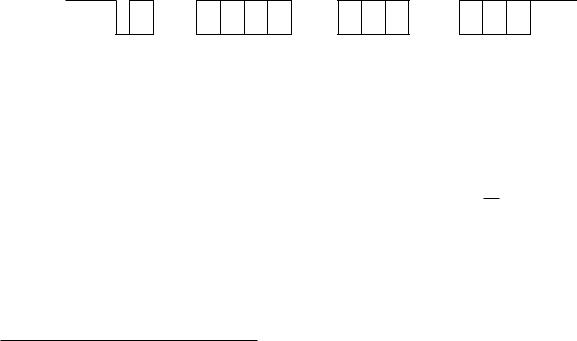
The general layout of an IIC packet is depicted in Figure 3.8.
S
A6
...
A0 R/W ACK D7
...
D0 ACK D7
...
D0 ACK P/Sr
Figure 3.8: An IIC frame.
In their idle states, both SCL and SDA are high. The transmission is initiated by the master, who puts out a clock signal on SCL and generates a start condition (S) on SDA. Then, the master puts the address on the bus and states whether this is a read access (that is, the addressed device should transfer data) or a write access (the master transfers data to the device). After the R/W bit, the slave sends an acknowledge to indicate that it has recognized its address. Depending on the data direction, either the master or the slave can now transmit an arbitrary number of data bytes. Each byte is acknowledged by the receiver (with the exception of the last byte if the master is the receiver). At the end of the transmission, the master either generates a STOP condition (P) to indicate that the bus is now free, or it can keep the bus by sending a repeated START condition (Sr), which ends the current transmission and at the same time starts a new one.
8Note that Atmel calls its IIC module Two-wire Interface (TWI).

3.3. IIC (I2C) |
85 |
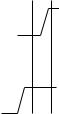
Start and Repeated Start
The START condition (S) is shown in Figure 3.9. It is characterized by a falling edge on the SDA line during a high level of the SCL line. Note that only the START and STOP conditions change the level of SDA during a high state of SCL. All normal data transmission including acknowledgements change the level during the low state of SCL.
SDA
SCL S
START condition
Figure 3.9: START condition (S).
The repeated START condition (Sr) is the same as the normal START condition. It replaces a STOP/START condition pair and is sent instead if the master intends to immediately use the bus again. In a single-master system, the Sr simply saves one clock cycle. In multi-master systems, the Sr prevents an arbitration phase (see Section 3.3.3) and thus ensures that the currently transmitting master keeps the bus.
Address
The 7-bit address is sent msb first. As with all normal data bits, the SDA level is changed during the low phase of SCL and is read during the high phase.
Direction Control
After the seven address bits, the master completes the byte with an eight bit (R/W) that indicates the direction of the subsequent transmission. If R/W is high, then the master wants to read data from the addressed slave. If the bit is low, the master intends to send data to the slave.
Note that every transmission on the bus is initiated by the master, who sends the slave address. If R/W is high, the slave sends its acknowledge. After that, data direction changes and the slaves starts transmitting data.
Acknowledgement
After every 8 bits, the receiver sends an acknowledge (ACK) to indicate that it has received the data. The ACK is achieved by setting SDA to low. The only exception is the final acknowledge of the master if it is the receiver: In that case, the master does not acknowledge the last byte, that is, SDA remains high. The high indicates to the transmitting slave that the end of the transmission has been reached. The slave then releases the data line to allow the master to transmit the repeated start or stop condition.
86 |
CHAPTER 3. COMMUNICATION INTERFACES |
Data
The data bits are transmitted like all other bits, and each byte must be acknowledged by the receiver. Data is transfered msb first. There is no limit on the number of data bytes that can be transmitted in one frame.
Stop
Figure 3.10 depicts the STOP condition (P). It mirrors the START condition, so SDA now goes from low to high while SCL is high.
SDA
SCL P
STOP condition
Figure 3.10: STOP condition (P).
The STOP condition (P) is transmitted by the master if it wants to give up the bus. As soon as the STOP condition has been sent, the bus is idle and can be requested by any master, see Section 3.3.3.
3.3.2Speed Control Through Slave
Since there is no way to negotiate the transmission speed between master and slave, the master simply transmits data with a fixed speed. Of course, the speed is matched to the specifications of the slave devices, but still it could occur that e.g. the slave needs some time to process data sent by the master. Hence, we need a means to tell the master to hold on for a while. The IIC protocol rather cleverly exploits the dominant/recessive nature of the clock line to provide speed control by the slave. Let us first define two phases of a clock signal: the low phase is the period during which the clock signal is low. Similarly, the high phase is the period during which the clock signal is high. To generate the signal, the master has to start the phase by an appropriate signal edge (rising or falling) and then wait until it is time to generate the next edge, just like a PWM signal is generated by the timer. Now to get speed control by the slave, the master does not generate its clock signal blindly, but reads back SCL and only starts timing the low resp. high phase after it has recognized a falling resp. rising edge on SCL. As a result, whenever the slave needs more time, it can simply set the clock line low. Since low is the dominant state, this will prolong the low time of the current clock tick and thus delay the master until the slave releases SCL. Since the master waits until the rising edge before timing the high phase, all subsequent clock cycles are just delayed but not affected.
This mechanism entails that IIC devices are pretty flexible as far as bit rate is concerned. Hence, the three speed modes provide maximum ratings, but the actual transmission speed on the bus can be arbitrarily low as long as the IIC bus timing constraints (which do not specify the duration of the clock cycles, but mostly deal with dependencies between the SDA and SCL lines) are met.