

3.1. SCI (UART) |
75 |
3.1 SCI (UART)
The Serial Communication Interface (SCI) provides an asynchronous communication interface (Universal Asynchronous Receiver Transmitter, UART). The UART module utilizes two wires, a transmit (TXD) and a receive (RXD) line, for fullor half-duplex communication.
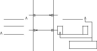
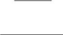
Figure 3.1 shows the internal structure of a UART. Basically, the module consists of a transmit and a receive register to hold the data. True to its asynchronous nature, transmission and reception on a node are driven by its local clock generator.
|
|
|
|
TX Register |
|||||
|
|
msb |
|
|
|
|
lsb |
||
|
|
|
|
|
|
|
|
|
|
|
|
|
|
|
|
|
|
|
|
|
|
|
|
|
|
|
|
|
|
|
|
lsb |
|
|
|
|
msb |
||
|
|
|
|
|
RX Register |
|
|
||
|
|
|
|
|
|
|
|||
|
|
|
|
|
|
|
|||
|
|
|
|
|
|||||
clock generator |
|
|
|||||||
|
|
|
|
|
|
|
|
|
|
TX RX
RX TX
|
RX Register |
||
msb |
|
|
lsb |
|
|
|
|
lsb |
TX Register |
msb |
clock generator
Figure 3.1: Basic structure of a UART module.
The UART is no communication protocol per se, but a module that can be used for asynchronous serial communication. Hence, the UART module within a microcontroller allows the application to control much of its behaviour. Configurable parameters include:
Number of Data Bits: Depending on the UART, the number of data bits can be chosen within a more or less wide range. The ATmega series, for example, allows between 5 and 9 data bits. Other UARTs may have a broader or smaller range.
Parity Bit: The user can select whether there should be a parity bit or not, and if yes, whether the parity should be odd or even. If the parity is set to even, the parity bit is 0 if the number of 1’s among the data bits is even. Odd parity is just the opposite.
Stop Bits: The user generally can select whether there should be one stop bit or two.
Baud Rate: The UART module contains a register which allows the user to select a certain baud rate (i.e., the transmission speed, given in bits per second (bps)) from a set of possible ones. Possible baud rates generally include the range within 9600 and 115200 baud. However, since the feasible baud rates depend on the frequency of the system clock, different clock speeds imply different sets of available baud rates.
The nomenclature used for describing the data format is D{E|O|N}S, where D is the number of data bits and S is the number of stop bits. E|O|N indicates even, odd, or no parity. For example, a data format with 8 data bits, even parity, and one stop bit is identified as 8E1. Note that there is no need to specify the number of start bits, since it is always one.
76 |
CHAPTER 3. COMMUNICATION INTERFACES |
Data Transmission
Messages are transmitted using Non Return to Zero (NRZ)3 encoding, that is, 1 corresponds to e.g. the more positive voltage and 0 corresponds to the more negative one (positive-logic) or vice versa (negative-logic). Since the communication is asynchronous, data has to be enveloped by a frame consisting of at least one start bit and one stop bit. Figure 3.2 shows the general frame format of a UART packet.
Start D0 D1
...
Dn (P) Stop (Stop)
Figure 3.2: UART frame format.
In its idle state, the line is high. A frame begins with a start bit, which causes the line to got low. This leading edge signals to the receiver that a new transmission has begun. After the start bit, the data bits are transmitted, beginning with the least significant bit. The number of data bits is configurable and must be set to the same value on both sender and receiver. After the data bits, there may follow one parity bit. The frame is concluded with one or two stop bits. Stop bits correspond to a high level.
Synchronization and Error Recognition
Since the communication is asynchronous, sender and receiver clocks are completely independent of each other. With the selection of the baud rate, the receiver knows what bit rate to expect, but it does not know when a bit starts and hence needs to synchronize to the falling edge of the start bit. Furthermore, clock oscillators tend to have a non-zero drift, that is, they deviate from their nominal frequency, so even if the receiver synchronizes to the sender clock at the start of the message, it might drift away during transmission.
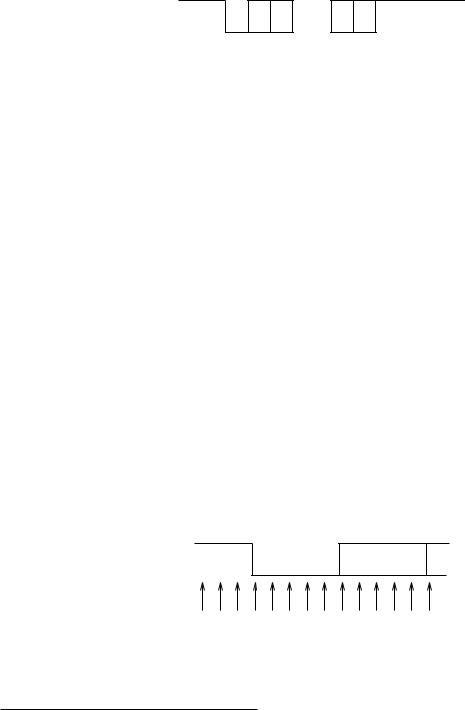
To gain initial synchronization to the sender, the receiver uses oversampling, that is, the RXD line is sampled s times per bit. A typical number for s is 16. When the receiver detects a falling edge, it assumes that this is the beginning of the start bit and begins counting the samples as depicted in Figure 3.3.
|
idle |
|
|
|
|
|
|
|
|
|
|
|
|
|
|
|
|
|
Start |
|
|
|
D0 |
|
|
|
|
0 |
0 |
0 |
1 |
2 |
3 |
4 |
5 |
1 |
2 |
3 |
4 |
5 |
1 |
Figure 3.3: UART bit sampling (s = 5).
3The name is derived from the Return to Zero encoding, where the voltage level returns to a “zero” state during the second half of each bit.
3.1. SCI (UART) |
77 |
Ideally, all s samples of the start bit should be zero. However, to be more resilient to noise, the UART only uses some of the samples to determine the value of the bit. The ATmega16, for example, has s = 16 and uses samples 8, 9, 10 and a majority vote to determine the state of the line. If two or more of the samples are high, the start bit is discarded as a spike on the line, otherwise it is recognized as the beginning of a transmission.
All subsequent bits of a packet are again sampled s times and the same technique as for the start bit is used to determine the bit value. The data bits are put into a receive shift register and are generally copied into a buffer register at the end of reception. The buffer register frees the shift register for the next data reception even if the application has not yet read the last data. The transmission is concluded with the stop bit(s).
There are some errors that may occur here: First of all, there may have been bit errors due to noise on the wire. If the packet included a parity bit, single bit errors (or more generally an odd number of bit errors) can be detected and are announced to the user. The data bits are still copied into the buffer register, but a parity error bit is set in the UART status register to indicate that there was a parity violation.
Secondly, it may occur that the baud rates of sender and receiver diverge too much, so that the receiver gradually lost synchronization during the transmission. This may be recognizable at the stop bit, where the UART expects to read a high level. If the stop bit was not recognized, a frame error is announced to the application. But of course there may be situations, e.g. when the receive clock is slow, where the idle state of the line is mistaken as the stop bit and the error is not recognized.
Finally, even though the UART generally uses a buffer register to give the application more time to read incoming data, so that a second transmission may begin before the data from the first was processed, it may occur that a third transmission is started before the data from the first message was read. In such a case, a data overrun occurs and the data in the shift register is lost. Such a data overrun is again indicated by a flag in the UART’s status register.
Baud Rate Generation
The baud rate is derived from the system clock by means of a counter. A baud rate register, which basically serves the same function as the output compare register described in Section 2.6.3, is used to generate a periodic clock signal. This signal is then scaled down (by s) to the desired baud rate using a prescaler. At the receiver, the same mechanism is used, but the clock signal is taken from before the prescaler. So the receiver samples s times faster than the bit rate. Since the sampling rate is generated from the receiver’s system clock, only signals with a bit rate of ≤ 1/s-th of the receiver clock rate can be handled.
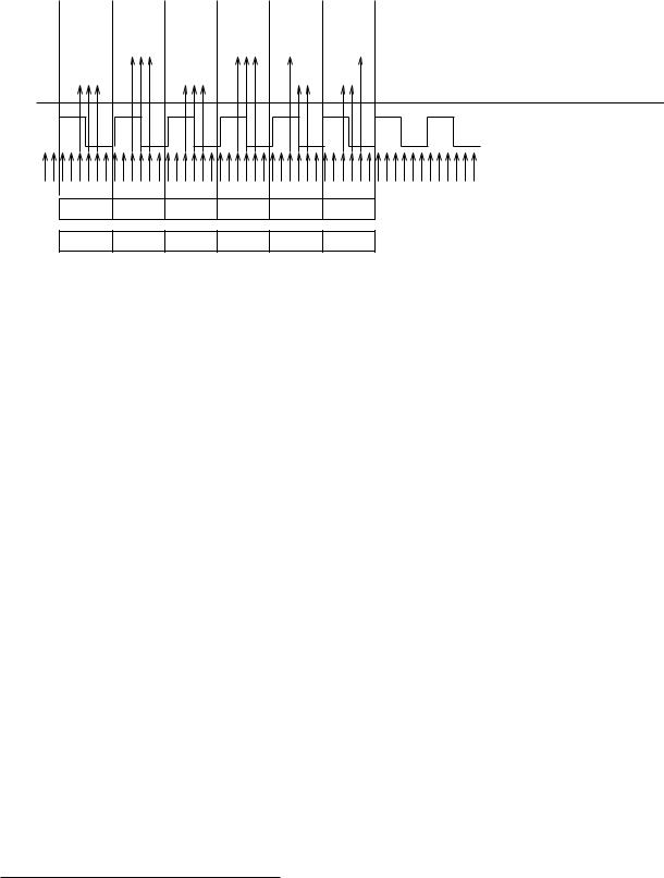
As a side-effect of generating the baud rate from the system clock, the set of baud rates offered by a controller depends on its clock frequency. Furthermore, not every arbitrary baud rate can be achieved exactly. For example, if we have an 8 MHz clock and use oversampling with s = 8, we can get a baud rate of 0.5 Mbps exactly. A baud rate of 115.2 kbps, on the other hand, cannot be generated by the controller’s system clock, since we would have to scale down the maximum achievable baud rate by (8 MHz/s)/115.2 kHz = 8.68. We can only set our counter to integer values, so any baud rate that has a fractional part here cannot be generated exactly. Figure 3.4 shows the consequence of a slower than expected transmitter baud rate on the receiver.
The example uses s = 6, with a frame format of 3E1. Samples 3, 4, and 5 are used for voting. The top half shows the transmitter view, the bottom half the receiver view. As you can see, the receiver
78 |
|
|
|
|
|
|
|
|
|
|
|
CHAPTER 3. COMMUNICATION INTERFACES |
|||||||
|
|
|
|
|
|
|
|
|
|
|
|
|
|
|
|
transmit clock (bit rate) |
|||
|
|
|
|
|
|
|
|
|
|
|
|
|
|
|
|
||||
|
|
|
|
|
|
|
|
|
|
|
|
|
|
|
|
|
|
|
Transmitter |
|
|
|
|
|
|
|
|
|
|
|
|
|
|
|
|
|
|
|
|
|
|
Start |
D0=1 |
D1=0 |
D2=1 |
P=0 |
|
Stop |
transmitted bits |
||||||||||
|
|
|
|
||||||||||||||||
|
|
|
|
|
|
|
|
|
|
|
|
|
transmitted signal |
|
|||||
|
|
|
|
|
|
|
|
|
|
|
|
|
|
|
|
|
|
|
|
receive clock (bit rate)
|
|
|
|
|
|
samples |
Receiver |
0 0 1 2 3 4 5 6 1 . . . |
|
|
|
|
|
|
|
Start |
D0 |
D1 |
D2 |
P |
Stop |
expected bits |
|
Start |
D0=1 |
D1=0 |
D2=1 |
P=0 |
0 ??? |
received bit values |
|
Figure 3.4: Baud rate of sender is too slow, receiver loses synchronization (3E1, s = 6).
synchronizes itself to the start bit and then gradually loses synchronization because it is faster than the transmit clock. Nevertheless, the data bits are still recognized correctly, even though the samples are not in the center of the transmitted bits, but move closer towards the left edge with every bit. Since the sampling algorithm uses a voting algorithm to determine the bit value, even the parity bit is still recognized correctly, even though the first of its samples has in fact read the value of data bit D2. Only at the stop bit does the receiver realize that something is amiss.
Still, had the sender been just a bit faster, or had we used a 2E1 data format, the receiver would have recognized the stop bit as well (even though perhaps inexactly, like the parity bit in our example). So apparently an exact match of sender and receiver clock is not necessary, as long as we keep the frequencies close enough together. It is also obvious that the longer the frame, the closer together the frequencies have to be, because the receiver must still be close enough at the stop bit to detect it correctly.
So if we come back to our example of B = 115.2 kbps with an f = 8 MHz clock and s = 8, we could set our counter to C = 9 because this is closest to the 8.68 we require4. The resulting baud rate
|
B0 = |
f |
|
(3.1) |
||
s · C |
||||||
diverges from the desired baud rate B by |
|
|||||
|
|
|
||||
|
B0 |
|
|
(3.2) |
||
( |
|
− 1) · 100%, |
||||
B |
||||||
so in our case we would get an error of -3.5% . To determine whether this is acceptable for our frame format, we have to compute how much the receive clock will diverge from the send clock during transmission. If the majority of samples taken for one bit fall into the stop bit, the transmission will be successful. If the majority of samples is outside, synchronization will be lost.
Let us assume that the sender operates with sampling frequency ft (so the bit rate is ft/s)5 and the receiver samples with frequency fr. From the s samples s0, · · · , ss−1 taken by the receiver, samples
4Note that e.g. on the ATmega16, this implies that the baud rate register has to be set to 8, because the counter starts at 8 and counts down to including zero, scaling the timer down to 1/9-th of its frequency.
5To simplify our computations, we use the sampling frequency and not the system clock frequency of the device here. If the system clock frequency is f, you get the sampling frequency by dividing through the counter value C.
3.1. SCI (UART) |
79 |
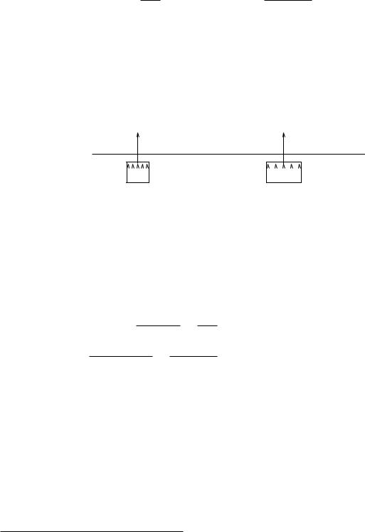
sv1 , . . . , sv2n+1 , 0 ≤ v1 < . . . < v2n+1 ≤ s − 1, are used for the voting algorithm6. As we can see in Figure 3.4, if a sample is taken from two different bits, then either the middle sample svn is taken
from the correct bit and the voting will decide on the correct value, or svn is taken from the wrong bit, in which case voting will fail. So for a receiver to recognize the k-th bit, k ≥ 0, of a frame correctly, sample svn must be from bit k. To ensure this, the following conditions have to be fulfilled:
k · s |
< k |
· |
s |
+ |
vn |
+ o < |
(k + 1) · s |
, |
(3.3) |
|
fr |
|
|
||||||
ft |
|
fr |
ft |
|
|||||
where o (0, 1/fr) is the offset of the first sample from the falling edge of the start bit.
Figure 3.5 illustrates the formula. If we assume that at the start of the transmission, t = 0, then
|
k |
|
|
|
|
|
|
|
|
|
ts |
= k |
· |
s/f |
falling edge of the start bit is |
||||||||||||
the start of bit |
|
at the sender is at |
k |
|
|
t. At the receiver, the |
r |
|
s/f |
+ o, and sample |
|||||||||||||||||
|
|
offset o |
|
|
(0, 1/f ). The start of bit k is expected at t = k |
· |
|||||||||||||||||||||
recognized with an r |
|
|
|
|
|
|
r |
|
|
|
|
|
|
|
|
|
|
|
k |
|
r |
||||||
svn is taken at time tk + vn |
· 1/fr. If this sample has to be taken from the transmitted bit k, Equ. (3.3) |
||||||||||||||||||||||||||
directly follows. |
|
|
|
|
|
|
|
|
|
|
|
|
|
|
|
|
|
|
|
|
|
|
|
|
|
|
|
|
|
|
|
|
|
|
|
|
bit k |
|
|
|
|
|
|
|
bit k |
Transmitter |
|
||||||||
|
|
|
|
|
|
|
|
|
|
|
|
|
|
|
|
|
|
|
|
|
|
|
|
|
|||
|
|
|
|
|
|
|
|
|
|
|
|
|
|
|
|
|
|
|
|
||||||||
|
|
|
|
bit k |
|
|
|
|
|
|
|
bit k |
|
|
|
|
|||||||||||
|
|
|
|
|
|
|
|
|
|
|
|
|
|
|
|
|
|
|
|
|
|
|
|
Receiver |
|
|
|
|
|
|
|
|
|
|
|
|
|
|
|
|
|
|
|
|
|
|
|
|
|
|
|
|
|
|
|
|
|
|
|
|
|
v |
n |
|
|
|
|
|
|
|
|
|
|
|
vn |
|
|
|
|
||||
|
|
|
|
fast receiver |
|
|
|
|
slow receiver |
|
|
|
|
||||||||||||||
Figure 3.5: Sampling the k-th bit of a frame.
Equ. (3.3) is useful for a number of things. For example, if we have a given frame length of k bits, we can now compute conditions for the relation of ft to fr. Equ. (3.3) gives us
|
|
k · s + vn |
> |
k · s |
|
fr |
|||||||
|
|
|
|
ft |
ft |
||||||||
|
|
|
|
fr |
|
|
|
|
|||||
|
k · s + vn + 1 |
< |
|
(k + 1) · s |
|
fr |
|||||||
|
|
|
ft |
ft |
|||||||||
|
fr |
|
|
|
|||||||||
which leads to the conditions |
|
|
|
|
|
|
|
|
|
||||
|
|
|
|
k |
|
+ |
vn + 1 |
|
< |
fr |
|
||
|
|
|
|
|
|
|
|
ft |
|||||
|
|
|
k + 1 (k + 1) · s |
||||||||||
< 1 + |
vn |
|
and |
|
|||
k · s |
|
||||||
|
|
k |
vn + 1 |
|
|||
> |
|
|
+ |
|
, |
||
|
|
|
|
|
|||
|
k + 1 (k + 1) · s |
|
|||||
< 1 + |
vn |
|
|
(3.4) |
|||
k · s |
|
||||||
|
|
|
|
|
|||
for the relation fr/ft. Note that for k → ∞, we get
klim k + 1 |
+ (k + 1) |
|
s! = 1 = klim |
1 + k |
s |
||||
|
k |
|
vn + 1 |
|
|
|
vn |
||
→∞ |
|
|
· |
|
→∞ |
· |
|
||
and hence limk→∞ fr/ft = 1, that is, send and receive frequencies should be equal, which is to be expected.
6We use an odd number here to ensure a majority. Adapting the formulas for an even number is left as an exercise to the reader.
80 |
CHAPTER 3. COMMUNICATION INTERFACES |
If ft and fr are given, then an upper bound on the frame length k might be of interest. Here, it is useful to note that the left inequality of Equ. (3.3) is important for fr > ft. In that case, the worst case is that o = 0. For fr ≤ ft, the left inequality is always true. Similarily, the right part is only important for fr < ft and always true otherwise. Here, the worst case is that o = 1/fr. So assuming given fr and ft, we get the conditions
k < |
|
vn · ft |
for fr > ft |
(3.5) |
|
|
s · (fr − ft) |
||||
|
|
|
|
|
|
and |
|
|
|
|
|
k < |
s · fr − (vn + 1) · ft |
for fr < ft. |
(3.6) |
||
|
|
s · (ft − fr) |
|
|
|
For fr = ft we have perfect synchronization and k = ∞.
Note that the above bounds are only valid under the assumption that there is no noise on the line. If spikes can occur, then some of the samples taken could have a wrong value. To tolerate e such erroneous samples, not only sample svn but samples svn−e, . . . , svn+e have to be taken from bit k and the upper and lower bounds of the previous equations have to be adapted accordingly.
RS-232
The UART itself is only the implementation of the asynchronous serial communication protocol but does not define any physical characteristics of the interface, like the voltage levels used. In the microcontroller, the bits are just mapped to the controller’s voltages for 0 and 1. With a suitable voltage translation device, however, a UART can be used with a wide range of physical interfaces. The most common one is the RS-232 standard which can be found in PCs.
The RS-232 is a single-ended serial connection intended for point-to-point communication. It defines communication equipment types, electrical specifications, signal lines and signal timing. The RS-232 standard provides for 25 lines (you probably know the 25-pin serial connectors), although PCs generally only use 9 of these lines (the well-known D-SUB9 connectors). Of these nine bits, only two (RXD and TXD) are used by the UART. A third (GND) is required because the connection is single-ended. The rest are control lines that can be used with more advanced communication protocols.
The RS-232 specification defines the signal voltage levels to be within ±3-15V, and devices must be able to withstand a maximum of ±25V. Control lines use positive logic, data lines use negative logic.
Since the microcontroller is not capable of handling the voltages required by the RS-232 interface, a conversion IC has to be used that translates the GND and VCC levels of the controller to the voltage levels used by the RS-232 and vice versa. In our lab, for example, we use a MAX232 for this purpose. The chip uses an internal charge pump to generate ±12V from a 5V supply voltage.
RS-422
The RS-422 standard is also designed for point-to-point communication, just like the RS-232. However, it uses differential lines (both RXD and TXD consist of twisted-pair wires) for transmission. Hence, it does not need a common GND wire. The RS-422 can be used instead of the RS-232 to extend the transmission range of the UART. It is also the better choice in noisy environments.
3.1. SCI (UART) |
81 |
USART
The Universal Synchronous Asynchronous Receiver Transmitter (USART) extends the functionality of the UART by a synchronous transmission module. The USART therefore has an additional third line which carries a clock signal. In synchronous mode, the clock signal is generated by one of the communication partners and is used by both for data transmission and reception. Naturally, this synchronous communication makes the oversampling mechanism of the asynchronous module unnecessary, so the synchronous mode is by a factor s faster than the asychronous mode. The USART module combines the logic for both synchronous and asynchronous communication. If asynchronous communication is used, the clock line is free and can generally be used as a normal digital I/O pin.
82 |
CHAPTER 3. COMMUNICATION INTERFACES |
3.2 SPI
The Serial Peripheral Interface (SPI)7 is a simple synchronous point-to-point interface based on a master-slave principle. It provides full-duplex communication between a master (generally a controller) and one (or more) slaves (generally peripheral devices). The interface consists of four lines:
MOSI (Master Out, Slave In): This line is used by the master to transmit data to the slave.
MISO (Master In, Slave Out): This line is used by the slave to transmit data to the master.
SCK (System Clock): This line is used by the master to transmit the clock signal.
SS (Slave Select): This line is used by the master to select a slave.
Figure 3.6 shows the basic principle of the SPI interface. Both the master and the slave have an internal shift register which is operated by SCK. At each clock pulse, the msb (or lsb, this is generally configurable) of the master’s SPI register is shifted out on the MOSI line and shifted into the slave’s SPI register as lsb. At the same time, the slave’s msb is transmitted over the MISO line into the master’s register as lsb. After 8 such clock cycles, master and slave have exchanged all eight bits in their registers.
Master |
|
MOSI |
|
Slave |
msb |
lsb |
MISO |
msb |
lsb |
|
||||
clock generator |
|
SCK |
|
& |
|
|
|
||
|
|
SS |
|
|
Figure 3.6: SPI interface.
The master must explicitly address the slave by setting SS to low. Hence, we can connect two slaves to the SPI if we let one of them react to SS directly, whereas the other first negates the line. By setting SS to low resp. high, the master can then select the first resp. the second slave.
If the master is prepared to use up more of its I/O pins, then the number of slaves can be extended to 2n for n addressing lines with the help of an external decoder.
7The SPI is also often used for programming a microcontroller and is therefore sometimes (erroneously) called Serial Programming Interface.
3.3. IIC (I2C) |
83 |
3.3 IIC (I2C)
The Inter-IC bus (IIC) is a synchronous bus that operates on a master-slave principle. It uses two wires SCL (Serial Clock Line) and SDA (Serial Data Line) for half-duplex communication. The protocol has been developed by Philips [Phi00] and is widely used for (short distance) communication between one or more controllers and peripheral devices.
The protocol specification distinguishes three speed modes: The standard mode encompasses transmission speeds up to 100 kbit/s, the fast mode extends this range to 400 kbit/s, and the highspeed mode increases the transmission rate to 3.4 Mbit/s. Due to the protocol’s properties, fast and high-speed devices can be mixed with devices of lower speed.
The protocol includes bus arbitration mechanisms and thus allows the co-existence of several masters. The role of master normally falls to the microcontroller, with all peripheral devices as simple slaves. In a system with several microcontrollers, you may choose for each controller whether it should be a master or a slave. The only condition is that there must be at least one master in the system.
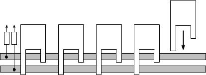
One of the main advantages of the IIC bus is its easy extensibility. New devices can be added to the bus by just connecting them, see Figure 3.7. There is no specific limit on the number of devices connected to the bus as long as the maximum bus capacitance of 400 pF is not exceeded.
VDD |
|
|
I/O |
|
|
|
|
MCU |
RTC |
AD/DA |
LCD |
SDA |
|
|
|
SCL |
|
|
|
Figure 3.7: Basic configuration of the IIC bus.
The IIC bus supports both 7-bit and 10-bit addresses. In 7-bit addressing all devices on the bus are identified by a 7-bit address, part of which (e.g. the highest 4 bit) are hard-coded by the manufacturer. The remaining bits can be programmed by the board designer. The addresses (0000XXX)2 and (1111XXX)2 are reserved, leaving 112 potential device addresses. To increase the number of addressable devices, the protocol was later extended to 10-bit addresses. Care was taken, however, to remain compatible to the original 7-bit addressing mode, so 7-bit address devices can still be used in the new addressing scheme. In this section, we will focus on the 7-bit addressing scheme. Details to 10-bit addressing can be found in the specification [Phi00].
We have not explicitly mentioned it until now, but it is obvious that the peripheral devices must already include an IIC (slave) interface to make the “plug-and-play” feature of Figure 3.7 possible. Manufacturers who wish to equip their devices with an IIC bus interface need to obtain a licence from Philips and can then incorporate the protocol into their devices. Likewise, microcontrollers sometimes