

22 |
CHAPTER 2. MICROCONTROLLER COMPONENTS |
2.2 Memory
In the previous chapter, you already encountered various memory types: The register file is, of course, just a small memory embedded in the CPU. Also, we briefly mentioned data being transferred between registers and the data memory, and instructions being fetched from the instruction memory.
Therefore, an obvious distinction of memory types can be made according to their function:
Register File: A (usually) relatively small memory embedded on the CPU. It is used as a scratchpad for temporary storage of values the CPU is working with - you could call it the CPU’s short term memory.
Data Memory: For longer term storage, generic CPUs usually employ an external memory which is much larger than the register file. Data that is stored there may be short-lived, but may also be valid for as long as the CPU is running. Of course, attaching external memory to a CPU requires some hardware effort and thus incurs some cost. For that reason, microcontrollers usually sport on-chip data memory.
Instruction Memory: Like the data memory, the instruction memory is usually a relatively large external memory (at least with general CPUs). Actually, with von-Neumann-architectures, it may even be the same physical memory as the data memory. With microcontrollers, the instruction memory, too, is usually integrated right into the MCU.
These are the most prominent uses of memory in or around a CPU. However, there is more memory in a CPU than is immediately obvious. Depending on the type of CPU, there can be pipeline registers, caches, various buffers, and so on.
About memory embedded in an MCU: Naturally, the size of such on-chip memory is limited. Even worse, it is often not possible to expand the memory externally (in order to keep the design simple). However, since MCUs most often are used for relatively simple tasks and hence do not need excessive amounts of memory, it is prudent to include a small amount of data and instruction memory on the chip. That way, total system cost is decreased considerably, and even if the memory is not expandable, you are not necessarily stuck with it: Different members in a MCU family usually provide different amounts of memory, so you can choose a particular MCU which offers the appropriate memory space.
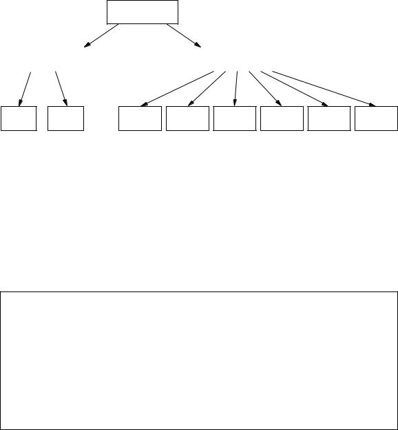
Now, the functional distinction of memory types made above is based on the way the memory is used. From a programmer’s perspective, that makes sense. However, hardware or chip designers usually view memory rather differently: They prefer to distinguish according to the physical properties of the electronic parts the memory is made of. There, the most basic distinction would be volatile versus non-volatile memory. In this context, volatile means that the contents of the memory are lost as soon as the system’s power is switched off.
Of course, there are different ways either type of memory can be implemented. Therefore, the distinction based on the physical properties can go into more detail. Volatile memory can be static or dynamic, and there is quite a variety of non-volatile memory types: ROM, PROM, EPROM, EEPROM, FLASH, NV-RAM. Let’s examine those more closely.
2.2. MEMORY |
23 |
Semiconductor
Memory
volatile |
|
non−volatile |
|
|
|
SRAM |
DRAM |
ROM |
PROM EPROM EEPROM |
Flash |
NVRAM |
EEPROM |
Figure 2.3: Types of Semiconductor Memory.
2.2.1Volatile Memory
As mentioned above, volatile memory retains its contents only so long as the system is powered on. Then why should you use volatile memory at all, when non-volatile memory is readily available?
The problem here is that non-volatile memory is usually a lot slower, more involved to work with, and much more expensive. While the volatile memory in your PC has access times in the nanosecond range, some types of non-volatile memory will be unavailable for milliseconds after writing one lousy byte to them.
Where does the name RAM come from?
For historic reasons, volatile memory is generally called RAM – Random Access Memory. Of course, the random part does not mean that chance is involved in accessing the memory. That acronym was coined at an early stage in the development of computers. Back then, there were different types of volatile memory: One which allowed direct access to any address, and one which could only be read and written sequentially (so-called shift register memory). Engineers decided to call the former type ‘random access memory’, to reflect the fact that, from the memory’s perspective, any ‘random’, i.e., arbitrary, address could be accessed. The latter type of memory is not commonly used any more, but the term RAM remains.
Static RAM
Disregarding the era of computers before the use of integrated circuits, Static Random Access Memory (SRAM) was the first type of volatile memory to be widely used. An SRAM chip consists of an array of cells, each capable of storing one bit of information. To store a bit of information, a so-called flip-flop is used, which basically consists of six transistors. For now, the internal structure of such a cell is beyond the scope of our course, so let’s just view the cell as a black box. Looking at Figure 2.4, you see that one SRAM cell has the following inputs and outputs:
Data In Din On this input, the cell accepts the one bit of data to be stored.
Data Out Dout As the name implies, this output reflects the bit that is stored in the cell.
24 |
CHAPTER 2. MICROCONTROLLER COMPONENTS |
Read/Write R/W Via the logical value at this input, the type of access is specified: 0 means the cell is to be written to, i.e., the current state of Din should be stored in the cell. 1 means that the cell is to be read, so it should set Dout to the stored value.
Cell Select CS As long as this input is logical 0, the cell does not accept any data present at Din and keeps its output Dout in a so-called high resistance state, which effectively disconnects it from the rest of the system. On a rising edge, the cell either accepts the state at Din as the new bit to store, or it sets Dout to the currently stored value.
Din |
|
SRAM |
|
|
|
|
|
||
R/W |
|
Memory |
|
Dout |
|
|
|||
CS |
|
Cell |
|
|
|
|
|
||
|
|
|
|
|
Figure 2.4: An SRAM cell as a black box.
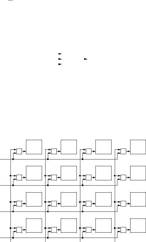
To get a useful memory, many such cells are arranged in a matrix as depicted in Figure 2.5. As you can see, all Dout lines are tied together. If all cells would drive their outputs despite not being addressed, a short between GND and VCC might occur, which would most likely destroy the chip. Therefore, the CS line is used to select one cell in the matrix and to put all other cells into their high resistance state. To address one cell and hence access one particular bit, SRAMs need some extra logic to facilitate such addressing (note that we use, of course, a simplified diagram).
|
SRAM Cell |
|
SRAM Cell |
|
SRAM Cell |
|
SRAM Cell |
||||
|
Din |
Dout |
|
Din |
Dout |
|
Din |
Dout |
|
Din |
Dout |
& |
R/W |
|
& |
R/W |
|
& |
R/W |
|
& |
R/W |
|
CS |
|
CS |
|
CS |
|
CS |
|
||||
row0 |
|
|
|
|
|
|
|
|
|
|
|
|
SRAM Cell |
|
SRAM Cell |
|
SRAM Cell |
|
SRAM Cell |
||||
|
Din |
Dout |
|
Din |
Dout |
|
Din |
Dout |
|
Din |
Dout |
& |
R/W |
|
& |
R/W |
|
& |
R/W |
|
& |
R/W |
|
CS |
|
CS |
|
CS |
|
CS |
|
||||
row1 |
|
|
|
|
|
|
|
|
|
|
|
|
SRAM Cell |
|
SRAM Cell |
|
SRAM Cell |
|
SRAM Cell |
||||
|
Din |
Dout |
|
Din |
Dout |
|
Din |
Dout |
|
Din |
Dout |
& |
R/W |
|
& |
R/W |
|
& |
R/W |
|
& |
R/W |
|
CS |
|
CS |
|
CS |
|
CS |
|
||||
row2 |
|
|
|
|
|
|
|
|
|
|
|
|
SRAM Cell |
|
SRAM Cell |
|
SRAM Cell |
|
SRAM Cell |
||||
|
Din |
Dout |
|
Din |
Dout |
|
Din |
Dout |
|
Din |
Dout |
& |
R/W |
|
& |
R/W |
|
& |
R/W |
|
& |
R/W |
|
CS |
|
CS |
|
CS |
|
CS |
|
||||
row3 |
|
|
|
|
|
|
|
|
|
|
|
col0 |
|
col1 |
|
|
col2 |
|
|
|
col3 |
|
|
Figure 2.5: A matrix of memory cells in an SRAM.
2.2. MEMORY |
25 |
As you can see in Figure 2.5, a particular memory cell is addressed (i.e., its CE pulled high) when both its associated row and column are pulled high (the little squares with the ampersand in them are and-gates, whose output is high exactly when both inputs are high). The purpose is, of course, to save address lines. If we were to address each cell with an individual line, a 16Kx1 RAM (16 K bits), for example, would already require 16384 lines. Using the matrix layout with one and-gate per cell, 256 lines are sufficient.
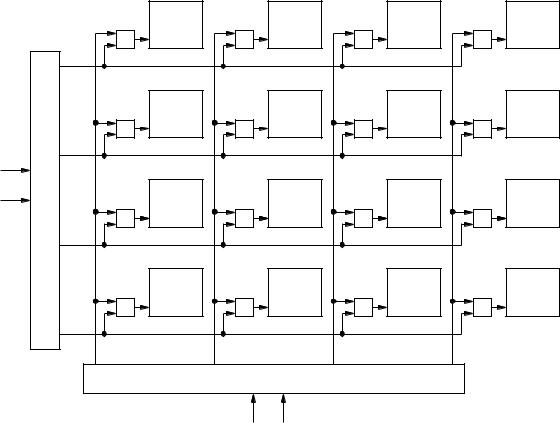
While 256 address lines is much better than 16384, it is still inacceptably high for a device as simple as a 16Kx1 RAM – such pin counts would make your common microcontroller pale in comparison. However, we can decrease the address line count further: No more than one row and one column can be selected at any given time – else we would address more than one memory cell at the same time. We can use this fact to reduce the number of necessary lines by adding so-called decoders. An n-bit decoder is a component with n input pins and 2n output pins, which are numbered O0 to O2n−1. At the input pins, a binary number b is presented, and the decoder sets Ob to 1 and all other outputs to 0. So, instead of actually setting one of many rows, we just need the number of the row we wish to select, and the decoder produces the actual row lines. With that change, our 16Kx1 SRAM needs no more than 14 address lines.
Figure 2.6 depicts our SRAM from Figure 2.5 after adding the decoder.
|
SRAM Cell |
|
SRAM Cell |
|
SRAM Cell |
|
SRAM Cell |
||||
|
Din |
Dout |
|
Din |
Dout |
|
Din |
Dout |
|
Din |
Dout |
& |
R/W |
|
& |
R/W |
|
& |
R/W |
|
& |
R/W |
|
CS |
|
CS |
|
CS |
|
CS |
|
||||
row0 |
|
|
|
|
|
|
|
|
|
|
|
|
SRAM Cell |
|
SRAM Cell |
|
SRAM Cell |
|
SRAM Cell |
||||
|
Din |
Dout |
|
Din |
Dout |
|
Din |
Dout |
|
Din |
Dout |
& |
R/W |
|
& |
R/W |
|
& |
R/W |
|
& |
R/W |
|
CS |
|
CS |
|
CS |
|
CS |
|
||||
row1 |
|
|
|
|
|
|
|
|
|
|
|
A0 |
SRAM Cell |
|
SRAM Cell |
|
SRAM Cell |
|
SRAM Cell |
||||
A1 |
Din |
Dout |
|
Din |
Dout |
|
Din |
Dout |
|
Din |
Dout |
R/W |
|
& |
R/W |
|
& |
R/W |
|
& |
R/W |
|
|
& |
CS |
|
CS |
|
CS |
|
CS |
|
|||
row2 |
|
|
|
|
|
|
|
|
|
|
|
|
SRAM Cell |
|
SRAM Cell |
|
SRAM Cell |
|
SRAM Cell |
||||
|
Din |
Dout |
|
Din |
Dout |
|
Din |
Dout |
|
Din |
Dout |
& |
R/W |
|
& |
R/W |
|
& |
R/W |
|
& |
R/W |
|
CS |
|
CS |
|
CS |
|
CS |
|
||||
row3 |
|
|
|
|
|
|
|
|
|
|
|
col0 |
|
|
col1 |
|
|
col2 |
|
|
col3 |
|
|
A2 A3
Figure 2.6: Further reducing the number of external address pins.
Of course, one cell may be composed of more than one flip-flop. To make a 256x4 SRAM, we would use an array of 16x16 cells, each containing four flip-flops.

26 |
CHAPTER 2. MICROCONTROLLER COMPONENTS |
So much for the internals of a SRAM. Now, what do we actually see from the outside? Well, a SRAM usually has the following external connections (most of which you already know from the layout of one memory cell):
Address Lines A0 . . . An−1 We just talked about these. They are used to select one memory cell out of a total of 2n cells.
Data In (Din) The function is basically the same as with one memory cell. For RAMs of width n ≥ 2, this is actually a bus composed of n data lines.
Data Out (Dout) Same function as in a single memory cell. Like Din, for RAMs of width n ≥ 2, this would be a bus.
Chip Select (CS) or Chip Enable (CE) This is what Cell Select was for the memory cell.
Read/Write (R/W ) Again, this works just like R/W in a memory cell.
Dynamic RAM
In contrast to a well known claim that nobody will ever need more than 640 kilobytes of RAM, there never seems to be enough memory available. Obviously, we would like to get as much storage capacity as possible out of a memory chip of a certain size.
Now, we already know that SRAM usually needs six transistors to store one single bit of information. Of course, the more transistors per cell are needed, the larger the silicon area will be. If we could reduce the number of components needed – say, we only use half as much transistors –, then we would get about twice the storage capacity.
That is what was achieved with Dynamic Random Access Memory – DRAM: The number of transistors needed per bit of information was brought down to one. This, of course, reduced the silicon area for a given cell count. So at the same chip size, a DRAM has much larger storage capacity compared to an SRAM.
How does that work? Well, instead of using a lot of transistors to build flip-flops, one bit of information is stored in a capacitor. Remember capacitors? They kind of work like little rechargeable batteries – you apply a voltage across them, and they store that voltage. Disconnect, and you have a loaded capacitor. Connect the pins of a loaded capacitor via a resistor, and an electrical current will flow, discharging the capacitor.
Now, where’s the one transistor per memory cell we talked about, since the information is stored in a capacitor? Well, the information is indeed stored in a capacitor, but in order to select it for reading or writing, a transistor is needed.
By now, it should be obvious how a DRAM works: If you want to store a logical one, you address the memory cell you want to access by driving the transistor. Then, you apply a voltage, which charges the capacitor. To store a logical zero, you select the cell and discharge the capacitor. Want to read your information back? Well, you just have to check whether the capacitor is charged or not. Simple.
Too simple, of course – there is a catch. Actually, there are a number of catches, the most annoying one being the fact that there is no perfect insulation on the chip. Once the capacitor is loaded, it should keep the charge – theoretically. However, due to the flow of minimal currents through the non-perfect insulators on the chip (so-called leakage currents), the capacitor loses its charge, despite not being accessed. And since these capacitors are rather small, their capacity is accordingly small. This means that after loading the capacitor, the charge will unavoidably decrease. After some time (in the range of 10 to 100 ms), the charge will be lost, and the information with it.
2.2. MEMORY |
27 |
So how did the engineers make DRAM work? Well, they kind of handed the problem over to the users: By accessing DRAM, the information is refreshed (the capacitors are recharged). So DRAM has to be accessed every few milliseconds or so, else the information is lost.
To remedy the refresh problem, DRAMs with built-in refresh logic are available, but that extra logic takes up a considerable portion of the chip, which is somewhat counter-productive and not necessarily needed: Often, the CPU does not need to access its RAM every cycle, but also has internal cycles to do its actual work. A DRAM refresh controller logic can use the cycles in between the CPUs accesses to do the refreshing.
DRAM has about four times larger storage capacity than SRAM at about the same cost and chip size. This means that DRAMs are available in larger capacities. However, that would also increase the number of address pins larger package to accommodate them higher cost. Therefore, it makes sense to reduce the number of external pins by multiplexing row and column number: First, the number of the row is presented at the address pins, which the DRAM internally stores. Then, the column number is presented. The DRAM combines it with the previously stored row number to form the complete address.
Apart from the need for memory refresh, there is another severe disadvantage of DRAM: It is much slower than SRAM. However, due to the high cost of SRAM, it is just not an option for common desktop PCs. Therefore, numerous variants of DRAM access techniques have been devised, steadily increasing the speed of DRAM memory.
In microcontrollers, you will usually find SRAM, as only moderate amounts of memory are needed, and the refresh logic required for DRAM would use up precious silicon area.
2.2.2Non-volatile Memory
Contrary to SRAMs and DRAMs, non-volatile memories retain their content even when power is cut. But, as already mentioned, that advantage comes at a price: Writing non-volatile memory types is usually much slower and comparatively complicated, often downright annoying.
ROM
Read Only Memories (ROMs) were the first types of non-volatile semiconductor memories. Did we just say write access is more involved with non-volatile than with volatile memory? Well, in the case of ROM, we kind of lied: As the name implies, you simply cannot write to a ROM. If you want to use ROMs, you have to hand the data over to the chip manufacturer, where a specific chip is made containing your data.
A common type of ROM is the so-called Mask-ROM (MROM). An MROM, like any IC chip, is composed of several layers. The geometrical layout of those layers defines the chip’s function. Just like a RAM, an MROM contains a matrix of memory cells. However, during fabrication, on one layer fixed connections between rows and columns are created, reflecting the information to be stored in the MROM.
During fabrication of an IC, masks are used to create the layers. The name Mask-ROM is derived from the one mask which defines the row-column connections.
PROM
Of course, using ROM is an option only for mass production – maybe tens of thousands of units, depending on the size of the MROM. For prototypes, the setup cost for such a production run is prohibitively expensive.
28 |
CHAPTER 2. MICROCONTROLLER COMPONENTS |
As an alternative, Programmable Read Only Memory (PROM) is available. These are basically matrices of memory cells, each containing a silicon fuse. Initially, each fuse is intact and each cell reads as a logical 1. By selecting a cell and applying a short but high current pulse, the cell’s fuse can be destroyed, thereby programming a logical 0 into the selected cell.
Sometimes, you will encounter so-called One Time Programmable (OTP) microcontrollers. Those contain PROM as instruction memory on chip.
PROMs and OTP microcontrollers are, of course, not suitable for development, where the content of the memory may still need to be changed. But once the development process is finished, they are well-suited for middle range mass production, as long as the numbers are low enough that production of MROMs is not economically feasible.
EPROM
Even after the initial development is finished and the products are already in use, changes are often necessary. However, with ROMs or OTP microcontrollers, to change the memory content the actual IC has to be replaced, as its memory content is unalterable.
Erasable Programmable Read Only Memory (EPROM) overcomes this drawback. Here, programming is non-destructive. Memory is stored in so-called field effect transistors (FETs), or rather in one of their pins called gate. It is aptly named floating gate, as it is completely insulated from the rest of the circuit. However, by applying an appropriately high voltage, it is possible to charge the floating gate via a physical process called avalanche injection. So, instead of burning fuses, electrons are injected into the floating gate, thus closing the transistor switch.
Once a cell is programmed, the electrons should remain in the floating gate indefinitely. However, as with DRAMs, minimal leakage currents flow through the non-perfect insulators. Over time, the floating gate loses enough electrons to become un-programmed. In the EPROM’s datasheet, the manufacturer specifies how long the memory content will remain intact; usually, this is a period of about ten years.
In the case of EPROMs, however, this limited durability is actually used to an advantage: By exposing the silicon chip to UV light, the process can be accelerated. After about 30 minutes, the UV light will have discharged the floating gates, and the EPROM is erased. That is why EPROMS have a little glass window in their package, through which the chip is visible. Usually, this window is covered by a light proof protective seal. To erase the EPROM, you remove the seal and expose the chip to intense UV light (since this light is strong enough to permanently damage the human eye, usually an EPROM eraser is used, where the EPROM is put into a light-proof box and then exposed to UV light).
Incidentally, often EPROMs are used as PROMs. So-called One Time Programmable EPROMs (OTP-EPROMs) are common EPROMs, as far as the chip is concerned, but they lack the glass window in the package. Of course, they cannot be erased, but since the embedded glass window makes the package quite expensive, OTP-EPROMS are much cheaper to manufacture. The advantage over PROM is that when going to mass production, the type of memory components used does not change. After all, the OTP-EPROM used for mass production is, in fact, an EPROM just like the one used in prototyping and testing, just without the little window. To go from EPROM to PROM would imply a different component, with different electrical characteristics and possibly even different pinout.
EEPROM
With EPROMs, the programming and in particular the erasing process is quite involved. To program them, a special programming voltage is used, which is usually higher than the operating voltage. To