

Low-power Interface
12.2.4Clock control sequence summary
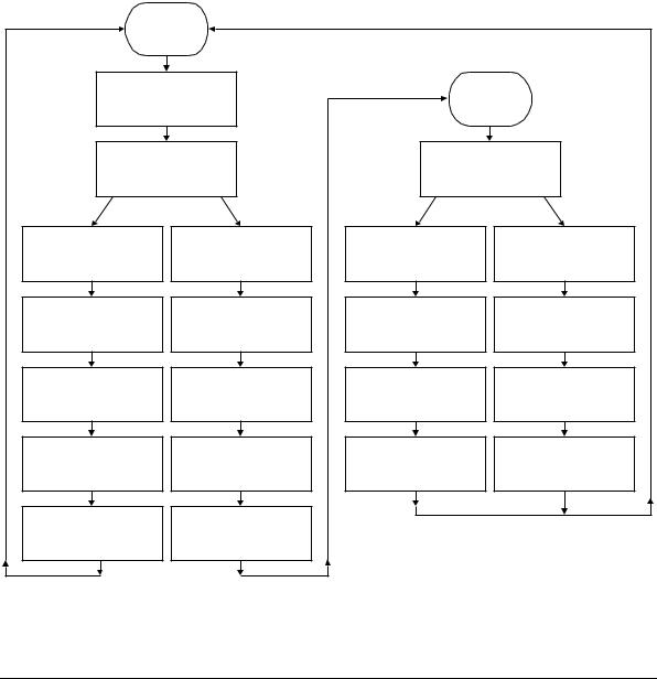
Figure 12-4 shows the typical flow for entering and exiting a low-power state.
Normal |
|
|
|
|
|
|
||
clocked |
|
|
|
|
|
|
||
operation |
|
|
|
|
|
|
||
System clock controller |
|
Low -pow er |
|
|||||
drives CSYSREQ low to |
|
unclocked |
|
|||||
request low -pow er |
entry |
|
operation |
|
||||
Peripheral |
denies |
or |
|
Peripheral |
or |
system |
|
|
|
clock controller |
initiates |
|
|||||
accepts |
request |
|
|
|||||
|
low -pow er |
exit |
|
|||||
|
|
|
|
|
||||
|
|
|
|
|
|
System clock |
||
Deny |
|
A ccept |
Peripheral |
|
|
controller |
||
|
|
|
|
|
|
|||
Peripheral keeps |
Peripheral perf orms |
Peripheral |
drives |
System clock controller |
||||
|
immediately |
enables |
||||||
CACTIV E HIGH |
|
pow er-dow n |
CACTIV E HIGH |
|
||||
|
|
clocks |
||||||
|
|
|
|
|
|
|||
Peripheral drives |
Peripheral drives |
System clock controller |
System clock controller |
|||||
CSYSACK LOW to |
immediately |
enables |
||||||
CACTIV E LOW |
drives CSYSREQ HIGH |
|||||||
acknow ledge request |
clocks |
|||||||
|
|
|
|
|
||||
System clock controller |
Peripheral drives |
System clock controller |
|
Peripheral |
drives |
|||
CSYSACK LOW to |
|
|||||||
samples CACTIV E |
drives CSYSREQ HIGH |
|
CACTIV E |
HIGH |
||||
acknow ledge request |
|
|||||||
|
|
|
|
|
|
|||
System clock controller |
System clock controller |
Peripheral |
drives |
|
Peripheral |
drives |
||
CSYSACK HIGH to |
|
CSYSACK HIGH to |
||||||
drives CSYSREQ HIGH |
samples CACTIV E |
|
||||||
complete handshake |
|
complete handshake |
||||||
|
|
|
|
|||||
Peripheral drives |
System clock controller |
|
|
|
|
|
||
CSYSACK HIGH to |
|
|
|
|
|
|||
disables clocks |
|
|
|
|
|
|||
complete handshake |
|
|
|
|
|
|||
|
|
|
|
|
|
|
||
Figure 12-4 Low-power clock control sequence
12-6 |
Copyright © 2003, 2004 ARM Limited. All rights reserved. |
ARM IHI 0022B |

Low-power Interface
12.2.5Combining peripherals in a low-power domain
The system clock controller can combine a number of different peripherals within the same low-power clock domain. Then the clock domain can be treated in the same way as a single peripheral if the following rules are observed:
•The clock domain CACTIVE signal is the logical OR of all the CACTIVE signals within the clock domain. This means that the system clock controller can disable the clocks only when all peripherals indicate that they can be disabled.
•The system clock controller can use a single CSYSREQ signal that is routed to all peripherals within the clock domain.
•The clock domain CSYSACK signal is generated as follows:
—the falling edge of CSYSACK occurs when the last falling edge from all of the peripherals occurs
—the rising edge of CSYSACK occurs when the last rising edge from all of the peripherals occurs.
ARM IHI 0022B |
Copyright © 2003, 2004 ARM Limited. All rights reserved. |
12-7 |

Low-power Interface
12-8 |
Copyright © 2003, 2004 ARM Limited. All rights reserved. |
ARM IHI 0022B |