

Embedded Systems Design - An Introduction to Processes Tools and Techniques (A. Berger, 2002)
.pdfwiggling. With rising excitement, more tests are run, and the chip seems to be doing okay. Next, some test software is loaded and executed. Rats! It died.
Without spending the next 20 pages on telling the story of this defect, assume that the defect is found in the code and fixed. Now what? Well, for starters, figure on $300,000 of nonrecoverable engineering (NRE) charges and about two months delay as a new chip is fabricated. Start-up companies generally budget for one such re-spin. A second re-spin not only costs the project manager his job but it often puts the company out of business. Thus, the cost penalty of a hardware defect is much more severe than the cost penalty of a software defect, even though both designers are writing software.
(The difference between the hardware issues now and in the past is that boardlevel systems could tolerate a certain amount of rework before the hardware designer was forced to re-spin the printed circuit board. If you’ve ever seen an early hardware prototype board, you know what I mean. Even if a revised board must be fabricated, the cost is still bearable — typically a few thousand dollars and a week of lost time. In fact, many boards went into production with “green wires” attached to correct last minute hardware defects. Usually the Manufacturing department had something like a “five green wire limit” rule to keep the boards from being too costly to manufacture. This kind Yof flexibility isn’t available when the traces on an IC are 180 billionths of a meter apart from each other.) Sometimes, you can compensate for a hardwareLdefect by revising the partitioning decision; simply repartition the algorithmFback towards the software and away from the defective hardware element. This might be a reasonable compromise, assuming the loss of performance associatedMwith the transfer from hardware to software is still acceptable (or theAarketing department can turn it into a new feature) and the product is not permanently crippled by it. However, suppose that a software workaround is notEacceptable, or worse yet, the defect is not a defect in the hardware design per se but is a defect in the interpretation of the hardware/software interface.TIn this case, you have the option of attempting to correct the defect in software if possible. However, if the defect is pervasive, you might lose just as much time, or more, trying to go back through thousands of lines of code to modify the software so that it will run with the hardware. Even though repartitioning can’t compensate for every hardware flaw, the cost penalty of a hardware re-spin is so great that every possible alternative is usually investigated before the IC design goes back to the vendor for another try.
Managing the Risk
Even though the hardware designer is writing software in silicon compilation, the expectations placed upon the hardware team are much greater because of what’s at stake if the hardware is defective. In fact, the silicon fabricators (foundry) won’t accept the design for fabrication unless a rather extensive set of “test vectors” is supplied to them along with the Verilog or VHDL code. The test vectors represent the ensemble of ones and zeros for as many possible input and output conditions as the engineer(s) can create. For a complex SoC, this can be thousands of possible combinations of inputs and outputs representing the behavior of the system for each clock cycle over many cycles of the system clock. The foundries require these vectors because they’ll ultimately need them to test the chips on their automated testers and because they want some assurance from the customer that the chip will work. The foundries don’t make profit from NRE charges; they want to sell the silicon that the customer has designed. This might be difficult for a software engineer to comprehend, but studies show that a hardware designer will spend 50 percent of the total project design time just in the process of design verification (creating test vectors). There are compelling arguments for investing a
Team-Fly®
similar testing effort in software. At Microsoft, for example, the ratio of development engineers to test engineers is close to one.
Before submitting the design to the foundry, the hardware designer uses the test vectors to run the design in simulation. Several companies in the business of creating the electronic design tools needed to build SoS provide Verilog or VHDL simulators. These simulators exercise the Verilog or VHDL design code and use the test vectors as the I/O stimulus for the simulation. With these powerful and expensive tools, the hardware design team can methodically exercise the design and debug it in much the same way as a software designer debugs code.
Traditionally, these simulators are used by the hardware design team. Again, the question is what if hardware and software design are the same process? If the VHDL simulator was available during the entire development process, it could be used, together with the VHDL or Verilog representation of the hardware, to create a virtual test platform. This virtual hardware could be exercised by the actual embedded software, rather than artificially constructed test vectors. This would allow the traditional hardware/software integration phase to be moved earlier in the process (or even eliminated).
For the hardware developer, this would certainly enhance the hardware/software integration process and provide an environment for better communications between the teams. Furthermore, uncertainties and errors in system specifications could be easily uncovered and corrected. For the software team, the gain is the elimination of the need to write stub code. In fact, the team could test the actual code under development against the virtual hardware under development at any point in the design process, testing hardware/software behavior at the module level instead of at the system level, which could be a big win for both teams.
Co-Verification
This vision of embedded system design in which the hardware and software teams work closely together throughout the design process is not especially new, but it has become much more important as SoCs have become more prevalent in embedded system design. The key has been the development of tools that form a bridge between the software realm (code) and the hardware realm (VHDL or Verilog simulation). The formal process is called codesign and co-verification. The names are often used interchangeably, but there is a formal distinction. Co-design is the actual process of developing the hardware and controlling software together. Co-verification tends to focus on the correctness of the hardware/software interface.
To understand how the co-design system works consider Figure 3.6.
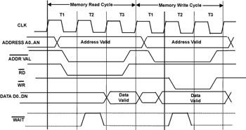
Figure 3.6: Memory bus cycle of microprocessors.
A memory bus cycle of a typical microprocessor. Each cycle of the clock, typically on a rising or falling edge, initiates different portions of the bus cycle.
In this particular example, which is representative of a generalized microprocessor, each processor bus operation (such as read or write) can be further subdivided into one or more clock cycles, designated as T1, T2 and T3. A hardware designer tasked with interfacing an ASIC design to a system containing this microprocessor might construct a set of test vectors corresponding to each rising and falling edge of the clock. Each vector would consist of the state of all the microprocessor’s signals, all the address bits, all the data bits, and all the status bits, complete with any additional timing information. A set of these vectors could then be used to represent a bus cycle of the processor, reading from or writing to the ASIC.
If you can do this, it would be easy to write a program that would convert a C or C++ assignment statement into the corresponding set of test vectors representing that bus cycle to the ASIC. Consider the following code snippet
*(unsigned int* ) 0xFF7F00A6 = 0x4567ABFF;
This instruction casts the address 0xFF7F00A6 as a pointer to an unsigned integer and then stores the data value 0x4567ABFF in that memory location. The equivalent assembly language instruction (68000) might be
MOVE.L |
#$4567ABFF, D0 |
LEA |
$FF7F00A6, A0 |
MOVE.L |
D0, (A0) |
From the hardware viewpoint, the actual code is irrelevant. The processor places the address, 0xFF7F00A6 on the address bus, places the data value 0x4567ABFF on the data bus at the appropriate point in the T states, and issues the WRITE command. If you construct a simulation model of this processor, you could then automatically generate a set of test vectors that would represent the data being written to the ASIC in terms of a series of I/O stimulus test vectors written to the VHDL or Verilog simulator. The program that does the translation from C or assembly code to test vectors is called a bus functional model and is the key element of any hardware/software co-design strategy. In theory, a bus functional model can be built for any commercially available microprocessor or microcontroller or for an embedded core, such as the ARM 7 TDMI processor that was discussed earlier. Figure 3.7 is a schematic representation of the entire process.
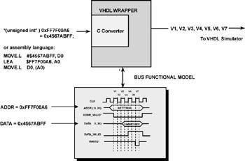
Figure 3.7: Conversion process.
To implement such a system, the C code snippets that actually access the hardware, such as in the example, must be replaced with a function call to the bus functional model. The function call contains all the information (read or write, address, data, bus width, and so on) necessary to construct a set of test vectors for the operation. On a read operation, the return value of the function is the result of the memory read operation.
If an Instruction Set Simulator (ISS) is used, assembly language code also can be used. The ISS must be able to trap the address accesses and then send the information to the bus functional model. A number of companies now offer such tools for sale (Seamless from Mentor Graphics, Eaglei from Synopsys, V-CPU from Summit Design are representative co-design and co-verification tools).
The conversion process from C or assembly language to VHDL or Verilog test vectors for ASIC simulation.
It would seem like this could be a boon to the SoC-development process. However, a number of challenges, both technological and economic, have prevented codesign and co-verification tools from achieving a broader market acceptance. For one, these tools are costly and complex to set up. For a team of software developers who are used to spending around $1,000 (or less) per user for a compiler and debugger, $50,000 per seat is a significant expense. Also, a VHDL simulator can cost $100,000 per seat; thus, it isn’t the type of tool that is used to equip a team of developers.
Second, the throughput of an Hardware Description Language (HDL) simulator can be very slow relative to the execution speed of the software stimulus. Although the software might be able to run at 25 million instructions per second on the workstation, the speed can drop to under 100 instructions per second when communicating with the simulator. The HDL simulator is very computer intensive; it must recalculate the entire state of the system on each clock cycle, for each set of test vectors, including all timing delays and setups. For a complex design of a million gates or so, even a powerful workstation can be slowed to a relative crawl. So, how bad is it? Figure 3.8 gives some approximate values for the percentage of time that software actually communicates directly with the hardware for various types of software accesses.
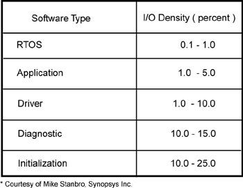
Figure 3.8: Instructions communicating directly.
Percentage of instructions ( I/O density) that communicate directly with hardware (courtesy of Mike Stansbro, Synopsys Corporation, Beaverton, Oregon).
As you might expect, the initialization of the hardware, typically at bootup or reset, has the highest percentage — as many as one in four instructions directly access the hardware. Application software and RTOS calls are the lowest, between 0.1 and 5 percent of the instructions. However, even if one instruction in a 1,000 must communicate with the simulator, the average slowdown is dramatic because the simulator is running many orders of magnitude slower than the software.
You might wonder whether any hard data indicates that co-verification is a viable technology. One case study[1] involves a manufacturer of telecomm and datacomm switching networks. The current design contained over one million lines of C source code. Prior to using the co-verification tools, the company’s previous design experience was disappointing. The predecessor was late to market and did not meet its original design specification. The company used a commercial coverification tool that was integrated with its RTOS of choice. The company focused its efforts on developing the hardware driver software while the ASICs were being designed and paid particular attention to verifying the correctness of the hardware/software interface specifications. As a result of this development strategy, product development time was cut from 16 months to 12 months, and the company realized a savings of $200,000–$300,000 in development costs. The company was so impressed with the results that it adopted hardware/software coverification as the corporate standard design practice.
Co-Verification and Performance
Figure 3.9 is a computer model that shows the expected performance of a coverification system. This simulation, an Excel spreadsheet model, assumes that the HDL simulator is running on a dedicated workstation, located remotely from the software being executed. Latency is five milliseconds for the round-trip time on the network. This is fairly typical of the use model for a co-verification environment. The simulator is running at 100Hz, and the instructions are plotted per second on the Y-axis (into the paper) over a range of 1,000 to 10,000,000 instructions per second. The X-axis (left to right across the paper) is the I/O density plotted over a
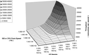
range of 5 percent down to 0.1 percent. The Z-axis is the resultant total throughput (instructions per second) for the simulation.
Figure 3.9: Throughput calculation.
Throughput as a function of Software Clock Speed and I/O Density for Remote Call Latency = 0.005 Sec, where hardware simulation rate = 100 Hz. Low I/O Density view.
It is apparent from the model that after the I/O density rises above 1%, the throughput is entirely limited by the speed of the HDL simulator (lightest gray surface). Only when the I/O density drops below 0.2 percent does the throughput rise above 10,000 instructions per second.
[1]Courtesy of Geoff Bunza, Synopsys Corporation.
Additional Reading
You can find more information about co-verification and co-design in the following sources:
Berger, Arnold. “Co-Verification Handles More Complex Embedded Systems.” Electronic Design, March 1998 (supplement), 9.
Leef, Serge. “Hardware and Software Co-Verification — Key to CoDesign.” Electronic Design, March 1998 (supplement), 18.
Morasse, Bob. “Co-Verification and System Abstraction Levels.”
Embedded System Programming, June 2000, 90.
Nadamuni, Daya. “Co-Verification Tools: A Market Focus.” Embedded System Programming, September 1999, 119.
Sangiovanni-Vincentelli, Alberto, and Jim Rowson. “What You Need to Know About Hardware/Software Co-Design.” Computer Design, August 1998, 63.
Tuck, Barbara. “The Hardware/Software Co-Verification Challenge.”
Computer Design, April 1998, 49.
Tuck, Barbara. “Various Paths Taken to Accelerate Advances in Hardware/Software Co-Design.” Computer Design, September 1998, 24.
Summary
The advances made in ASIC fabrication technology have elevated the issue of system design to a much greater prominence. Previously, when systems were designed at the board level and hardware designers chose from the catalog pages of available devices, the portioning decisions were rather limited. New ASIC and SoC options have greatly complicated the partitioning decision and radically changed the risk associated with defects.
The solution might evolve from the same force that generated this complexity. I believe in the near future, you’ll see a convergence of the hardware/software partitioning database with the hardware/software coverification tools to form an integrated tool suite that will allow a complete design cycle from partition to integration in one continuous process. These tools will allow designers to delay many partitioning decisions until the impact can be explored using virtual hardware.
Whether it’s sociological or traditional, embedded systems designers tend to draw a sharp distinction between the designers of hardware and the designers of software. Justified by this distinction, organizations have imposed varying degrees of separation between the teams. In an extreme case, the hardware might be built at a facility in another country and then shipped along with the hardware specification document to the software team for integration.
As hardware and software representations, tools, and processes converge, the justification will dwindle for this distinction — or for any separation between the teams.
Works Cited
1.Small, Charles H. “Partitioning Tools Play a Key Role in Top-Down Design.” Computer Design, June 1998, 84.
2.Mead, Carver, and Lynn Conway. Introduction to VLSI Systems. Reading, MA: Addison-Wesley, 1980.
Chapter 4: The Development
Environment
Overview
Modern desktop development environments use remarkably complex translation techniques. Source code is seldom translated directly into loadable binary images. Sophisticated suites of tools translate the source into relocatable modules, sometimes with and sometimes without debug and symbolic information. Complex, highly optimized linkers and loaders dynamically combine these modules and map them to specific memory locations when the application is executed.
It’s amazing that the process can seem so simple. Despite all this behindthe- scenes complexity, desktop application developers just select whether they want a free-standing executable or a DLL (Dynamic Link Library) and then click Compile. Desktop application developers seldom need to give their development tools any information about the hardware. Because the translation tools always generate code for the same, highly standardized hardware environment, the tools can be preconfigured with all they need to know about the hardware.
Embedded systems developers don’t enjoy this luxury. An embedded system runs on unique hardware, hardware that probably didn’t exist when the development tools were created. Despite processor advances, the eventual machine language is never machine independent. Thus, as part of the development effort, the embedded systems developer must direct the tools concerning how to translate the source for the specific hardware. This means embedded systems developers must know much more about their development tools and how they work than do their application-oriented counterparts.
Assumptions about the hardware are only part of what makes the application development environment easier to master. The application developer also can safely assume a consistent run-time package. Typically, the only decision an application developer makes about the run-time environment is whether to create a freestanding EXE, a DLL, or an MFC application. The embedded systems developer, by comparison, must define the entire runtime environment. At a minimum, the embedded systems developer must decide where the various components will reside (in RAM, ROM, or flash memory) and how they will be packaged and scheduled (as an ISR, part of the main thread, or a task launched by an RTOS). In smaller environments, the developer must decide which, if any, of the standard run-time features to include and whether to invent or acquire the associated code.
Thus, the embedded systems developer must understand more about the execution environment, more about the development tools, and more about the run-time package.
The Execution Environment
Although you might not need to master all of the intricacies of a given instruction set architecture to write embedded systems code, you will need to know the following:
How the system uses memory, including how the processor manages its stack
What happens at system startup
How interrupts and exceptions are handled
In the following sections, you’ll learn what you need to know about these issues to work on a typical embedded system built with a processor from the Motorola 68000 (68K) family. Although the details vary, the basic concepts are similar on all systems.
Memory Organization
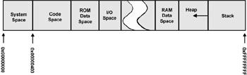
The first step in coming to terms with the execution environment for a new system is to become familiar with how the system uses memory. Figure 4.1 outlines a memory map of a generic microprocessor, the Motorola 68K (Even though the original 68K design is over 20 years old, it is a good architecture to use to explain general principles).
Figure 4.1: Memory map of processor.
Memory model for a 68K family processor.
Everything to the left of I/O space could be implemented as ROM. Everything to the right of I/O space can only be implemented in RAM.
System Space
The Motorola 68K family reserves the first 1,024 memory locations (256 long words) for the exception vector tables. Exception vectors are “hardwired” addresses that the processor uses to identify which code should run when it encounters an interrupt or other exception (such as divide by zero or overflow error). Because each vector consumes four bytes (one long word) on the 68K, this system can support up to 256 different exception vectors.
Code Space
Above the system space, the code space stores the instructions. It makes sense to make the system space and the code space contiguous because you would normally place them in the same physical ROM device.
Data Space
Above the code space, the ROM data space stores constant values, such as error messages or other string literals.
Above the data space, the memory organization becomes less regular and more dependent on the hardware design constraints. Thus, the memory model of Figure 4.1 is only an example and is not meant to imply that it should be done that way. Three basic areas of read/write storage (RAM) need to be identified: stack, free memory, and heap.
The Stack
The stack is used to keep track of the current and all suspended execution contexts. Thus, the stack contains all “live” local or automatic variables and all function and interrupt “return addresses.” When a program calls a function, the address of the instruction following the call (the return address) is placed on the stack. When the called function has completed, the processor retrieves the return address from the stack and resumes execution there. A program cannot service an interrupt or make a function call unless stack space is available.
The stack is generally placed at the upper end of memory (see Figure 4.1) because the 68K family places new stack entries in decreasing memory addresses; that is, the stack grows downwards towards the heap. Placing the stack at the “right” end of RAM means that the logical bottom of the stack is at the highest possible RAM address, giving it the maximum amount of room to grow downwards.
Free Memory
All statically allocated read/write variables are assigned locations in free memory. Globals are the most common form of statically allocated variable, but C “statics” are also placed here. Any modifiable variable with global life is stored in free memory.
The Heap
All dynamically allocated (created by new or malloc()) objects and variables reside in the heap. Usually, whatever memory is "left over" after allocating stack and free memory space is assigned to the heap. The heap is usually a (sometimes complex) linked data structure managed by routines in the compiler’s run-time package.
Many embedded systems do not use a heap.
Unpopulated Memory Space
The “break” in the center of Figure 4.1 represents available address space that isn’t attached to any memory. A typical embedded system might have a few megabytes of ROM-based instruction and data and perhaps another megabyte of RAM. Because the 68K in this example can address a total of 16MB of memory, there’s a lot of empty space in the memory map.
I/O Space
The last memory component is the memory-mapped peripheral device. In Figure 4.1, these devices reside in the I/O space area. Unlike some processors, the 68K family doesn’t support a separate address space for I/O devices. Instead, they are assumed to live at various addresses in the otherwise empty memory regions between RAM and ROM. Although I’ve drawn this as a single section, you should not expect to find all memory-mapped devices at contiguous addresses. More likely, they will be scattered across various easy-to-decode addresses.
Detecting Stack Overflow
Notice that in Figure 4.1 on page 71, the arrow to the left of the stack space points into the heap space. It is common for the stack to grow down, gobbling free memory in the heap as it goes. As you know, when the stack goes too far and begins to chew up other read/write variables, or even worse, passes out of RAM