

Embedded Systems Design - An Introduction to Processes Tools and Techniques (A. Berger, 2002)
.pdfactive interest in the selection process. Second, software and tool support must be an important part of the decision. The entire design team (including the software designers) must be involved in the selection because they are the ones who feel the pressure from upper management to “get that puppy out the door.” If the task of selecting the best processor for the job is left to the hardware designers with little consideration of the quality of the software and support tools, it might not matter that you had the best paper design if you missed your market window with a product that never got out of the lab.
Works Cited
1. Barr, Michael. “Choosing a Compiler: The Little Things.” Embedded Systems Programming, May 1999, 71.
2. Corrigan, Wilfred J. A speech at 1997 IP Forum in Tokyo, Japan. Reported in EE Times, 24 November 1997.
3. |
Halfhill, Tom R. “EEMBC Releases First Benchmarks.” Microprocessor |
|||
|
Report, May 2000. |
|
|
Y |
|
|
|
|
|
4. |
Hawley, Greg. “Selecting a Real-Time Operating System.” Embedded |
|||
|
|
|
L |
|
|
Systems Programming, March 1999, 89. |
|
||
|
|
|
F |
|
5. |
Mann, Daniel and Paul Cobb. “When Dhrystone Leaves You High and |
|||
|
Dry.” EDN, 21 May 1998 |
|
M |
|
|
|
|
|
|
|
|
A |
|
|
|
E |
|
||
|
T |
|
|
|
Team-Fly®
Chapter 3: The Partitioning Decision
Overview
Designing the hardware for an embedded system is more than just selecting the right processor and gluing it to a few peripherals. Deciding how to partition the design into the functionality that is represented by the hardware and the software is a key part of creating an embedded system. This decision is not just an academic exercise nor is it self-evident. You don’t just pick a processor, design the hardware, and then throw it over the wall to the software team. (Actually, many R&D labs still select a processor, design the hardware, and throw it over the wall, but the purpose of this chapter is to show you a better way.) The partitioning choice has significant impact on project cost, development time, and risk.
This chapter will explore the following:
The hardware/software duality that makes the partitioning decision possible
How the separation of hardware and software design imposes development costs
How silicon compilation is making the partitioning decision more flexible but more risk-laden
How future trends might radically alter your view of the partitioning decision
Hardware/Software Duality
Partitioning is possible and necessary because of the duality between hardware and software. For example, prior to the introduction of the 80486 by Intel, the hottest processor around was the 80386.
The 386 is an integer-only processor. To speed up your spreadsheet calculations, you purchased an 80387 numeric FPU processor. Systems without the FPU would detect that floating-point calculations were required and then simulate the presence of the FPU by branching to subroutines that performed the FPU functions, albeit much more slowly. The 387 performed floating-point calculations directly in hardware, rather than going through the much slower process of solving them in software alone. This difference often made the calculations 10 times faster.
This is an example of the partitioning problem. The 387 is more expensive than the 386. A cost-sensitive design won’t include it because fast floating-point calculations are probably not a necessary requirement of a costconscious user. However, the absence of the 387 does not prevent the user from doing floatingpoint calculations; it just means the calculations won’t be completed as rapidly as they could be if a FPU was available, either as a separate processor or as part of the processor itself (486).
For a second example, consider that any serious “gamer” (PC games player) worth his salt has the hottest, baddest video accelerator chip in his PC. Without the chip, software is responsible for the scene rendering. With the video accelerator, much of the rendering responsibilities are moved to the hardware. Without the accelerator, PC games don’t have the same impact. They are slow and don’t
execute smoothly, but they do execute. A faster CPU makes a big difference, as you would expect, but the big payback comes with the latest graphics accelerator chip. This is another example of a partitioning decision, this time based upon the need to accelerate image processing in real time.
Recall Figure 1.3 of Chapter 1. It describes a laser printer as an algorithm. The algorithm is to take a digital data stream, a modulated laser beam, paper, and carbon-black ink (soot) as inputs and then output characters and graphics on a printed page. The algorithm’s description didn’t specify which parts were based on specialized hardware and which were under control of the software.
Consider one aspect of this process. The data stream coming in must be transformed into a stream of commands to the laser system as it writes its beam on the surface of the photosensitive drum that transfers ink to paper. The beam must be able to be turned on and off (modulated) and be steered to create the 1,200 dots per inch (dpi) on the page. Clearly, this can be accomplished in the software or in the hardware via a specialized ASIC.
The complexity of the partitioning problem space is staggering. To fully describe the problem space, you would need dimensions for multiple architectures, target technologies, design tools, and more. Today, many systems are so complex that computer-aided partitioning tools are desperately needed. However, Charles H.
Small describes the partitioning decision process like this: “In practice, the analysis of trade-offs for partitioning a system is most often an informal process done with pencil and paper or spreadsheets.”[1]
Ideally, the partitioning decision shouldn’t be made until you understand all the alternative ways to solve the problem. The longer you can delay making the decision, the more likely you’ll know which parts of the algorithm need to be in hardware and which can be performed adequately in software. Adding hardware means more speed but at a greater cost. (It isn’t even that black and white, because adding more software functionality means more software to develop, more software in the system (bigger ROMs), and potentially a rippling effect back through the entire processor selection process.) Adding hardware also means that the design process becomes riskier because redesigning a hardware element is considerably more serious than finding a software defect and rebuilding the code image.
The fundamental problem, however, is that usually you can’t debug your system until the hardware is available to work with. Moreover, if you delay the decision too long, the software team is left idle waiting for the hardware team to complete the board.
Tip You don’t literally need to have the hardware to begin testing. The software team always has a number of options available to do some early-stage testing. If the team is working in C or C++, it could compile and execute code to run on the team’s PCs or workstations. Interactions with the actual hardware — such as reading and writing to memory-mapped I/O registers
— could be simulated by writing stub code. Stub code is a simple function that replaces a direct call to nonexistent hardware with a function call that returns an acceptable value so that the controlling software can continue to execute.
This method also works well with the evaluation boards that the semiconductor manufacturer might supply. Having the actual chip means that the code can be
compiled for the target microprocessor and run in the target microprocessor’s environment. In both cases, some incremental amount of code must be written to take the place of the non-existent hardware. Generally, this subcode (also called throwaway code) is based on some published hardware specification, so the danger of human error exists as well. If the degree of realism must be high, a large quantity of this throw-away code is written to accurately exercise the software, thus driving up the cost of the project. If the team can afford to wait for the actual hardware, the stub code can be cursory and skeletal at best.
Hardware Trends
In some ways, the partitioning decision was simpler in the past because hardware implementations of all but the simplest algorithms were too costly to consider. Modern IC technology is changing that fact rapidly.
Not too long ago, companies such as Silicon Graphics and Floating Point Systems made extremely expensive and complex hardware boxes that would plug into your DEC VAX or Data General Nova, and perform the hardware graphics and floatingpoint support that is now taken for granted in every desktop computer. Today, you can put entire systems on a single IC large enough, quantities of which can cost only a few dollars.
For example, AMD now produces a complete PC on a single chip, the SC520. The SC520 is designed around a 486 microprocessor “core” with all the peripheral devices that you might find in your desktop PC. Many of today’s amazingly small and powerful communication and computing devices — such as PDAs, cell phones, digital cameras, MPEG players and so on — owe their existence to ASIC technology and systems-on-silicon.
Figure 3.1 shows how board-level designs are migrated to both a group of ASIC devices and discrete microprocessors or to complete systems on a single chip. This figure also shows a rough estimate of the number of equivalent hardware “gates” that are possible to design into the ASIC with the IC design geometries that are shown. Today, 0.18 micron geometries represent the mainstream IC fabrication capabilities. Soon, that number will be 0.13 micron geometries, and 0.08 micron technology is currently under development. Each “shrink” in circuit dimensions represents greater circuit density, roughly going as the inverse square of the geometry ratio. Thus, going from 0.35 micron to 0.18 micron represented a fourfold increase in the total gate capacity of the chip design. Shrinking geometries mean greater speed because transistors are ever more closely packed, and smaller devices can switch their states faster than larger devices. (My apologizies to the electrical engineers who are cringing while they read this, but without a complete discussion of capacitance, this is as good as it gets.)
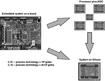
Figure 3.1: Evolution of SoS.
Board-level designs are migrating to processors plus ASICs and to complete systems on a single silicon die.
Along with the shrinking geometries is the increasing size of the wafers on which the ASIC dies are placed. Because much of the cost of fabricating an IC can be attributed to processing a wafer, the larger the wafer, the more dies can be cut from the wafer and the lower the cost per die. Thus, the technology is rapidly building on itself. Advances in IC fabrication technology enable designers to create devices that run at even greater speeds with greater design complexity, thus providing even more opportunities for the design and deployment of SoS.
Much of the technology leap can be traced back to the work of Carver Mead and Lynn Conway[2] on silicon compilation detailed in their book entitled Introduction to VLSI Design. Prior to their efforts, IC design was a laborious process. ICs were designed at the gate level, and building complex circuits required huge design teams.
Silicon compilation changed all that. In a manner similar to the process used today for software development, a hardware design is created as source code, using C- like languages, such as VHDL or Verilog. These source files are then compiled, just as a C or C++ program might be compiled. However, the output is not object code, rather, it’s a description language for how to build the IC, using the processes and design libraries of a particular IC vendor, or “silicon foundry.” Thus, just as a C compiler parses your source code down to the appropriate tokens and then replaces the tokens with the correct assembly language blocks, the silicon compiler creates a description of the circuit block and interconnects between those blocks so that a foundry can fabricate the masks and actually build the chip. All modern microprocessors are fabricated using Verilog or VHDL.
“Coding” Hardware
The simple example in Figure 3.2 illustrates how closely hardware description languages relate to traditional programming languages. A logical AND function is represented in three forms. In the first, familiar to most software engineers, you declare that A and B are Boolean input variables, and C is the resultant Boolean output variable, whose value is determined by the function C = AND (A,B). Because A, B, and C are Boolean, they represent a single digital value on a wire or printed circuit trace.
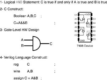
Figure 3.2: Another view of hardware/software duality.
The basic AND function is shown implemented as (2) a C construct, (3) a discrete hardware implementation using standard ICs, and (4) a hardware description language representation in Verilog.
The hardware designer recognizes the function C = A AND B as a logical equation that can be implemented using a standard AND gate — such as the 7408 — which contains four, two-input AND gates in a single 14-pin package. Circuits such as the 7408 have formed the "glue logic" in millions of digital systems over the past 25 years.
The Verilog representation of the same logical function is the last construct and is less familiar to most. A and B are signals on wires, and C represents the "register" that stores the result, A AND B. All three systems implement the same logical function, and C is always true if A and B are both true. However, the hardware implementations will be significantly faster, even in this simple-minded example. In the case of the C solution, A and B are perhaps local variables stored on the stack frame (local stack) of the function that is implementing the AND equation. Assuming a RISC processor with one operation per clock cycle and a cached stack frame, the processor must transfer both variables into separate registers (two instructions), perform the AND operation (one cycle), and then return the value in the appropriate register (more cycles). In the hardware implementation, the speed of the operation depends on either the propagation delay through the AND gate or, at worst, the arrival of the next clock signal.
Merging Hardware and Software Design
Because the hardware and the software design processes seem to be merging in their technology, you might wonder whether the traditional embedded design process is still the best approach. If the hardware design process and the software design process are basically identical, why separate the teams from each other? You’ve probably heard the phrase, “Throw it over the wall,” to describe how the hardware design is turned over to the firmware and application software developers. By the time the software developers start finding “anomalies,” the hardware designers have moved onto a new project.
Recently, several commercial products have come to market that attempt to address this new reality in the design process. “Hardware/software co-verification” is the term given to the process of more tightly integrating the hardware and software design processes. In hardware/software co-verification, the hardware, represented by Verilog or VHDL code, becomes a virtual hardware platform for the software. For example: Suppose the hardware specification given to the software team represents one of the hardware elements as a memory-mapped register block consisting of 64 consecutive 32-bit wide registers. (Registers can consist of various fields of width from 1 bit to 32 bits. Registers can be read-only, writeonly, or read/write.)
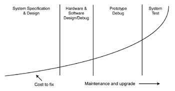
In the absence of real hardware, the software developers write stub code functions to represent the virtual behavior of the hardware that isn’t there yet. The software team usually spends a minimal amount of time and energy creating this throwaway code. Extensive software-to-hardware interface testing doesn’t begin until real hardware is available, which is a lost opportunity. The later you are in a project when a defect is discovered, whether it is a hardware defect or a software defect, the more expensive it is to fix as illustrated in Figure 3.3.
Figure 3.3: Where design time is spent.
The percentage of project time spent in each phase of the embedded design life cycle. The curve shows the cost associated with fixing a defect at each stage of the process.
Slightly over half the time is spent in the implementation and debug (hardware/software integration) phase of the project. Thus, you can save a lot in terms of the project’s development costs if you expose the hardware under development to the controlling software and the software under development to the underlying hardware as early as possible. Ideally, you could remove the “over the wall” issues and have a design process that continually exercises the hardware and software against each other from creation to release.
Figure 3.4 shows how the earlier introduction of hardware/software integration shortens the design cycle time. Much of the software development time is spent integrating with the hardware after the hardware is available.

Figure 3.4: Shortening the design cycle.
Schematic representation of the embedded design cycle showing the advantage of earlier integration of the software under development with the virtual hardware also under development.
The ASIC Revolution
Silicon compilation provided much more than a way for CPU designers to design better microprocessors and microcontrollers. Everyone who wanted to design an IC for any purpose could do so. Suddenly, anyone could design an IC that was specific to a particular function. Thus was born the ASIC. ASICs are the modern revolution in embedded-systems design. The chipsets that support the processor in your PC — the sound chip, the graphics accelerator, the modem chip — are all examples of ASICs that are widely used today. ASICs are also the technology of the SoC revolution that is still being sorted out today.
With silicon compilation, both hardware and software can be represented as compilable data files. Now, you can describe complete embedded systems in terms of a single software database. A portion of that software describes the fabrication of the hardware, and another portion of that software ultimately controls the hardware. The key point is that the distinction between what was once described as software and what was once described as hardware is blurring. Hardware design begins to look like software design that uses a different compiler (see Figure 3.5).
Figure 3.5: Hardware/software distinction blurring.
Hardware/software design flow. Notice the similarity between the activities followed by each design team.
Finally, just as the software designer can purchase a software library from a thirdparty vendor, the SoC designer can purchase hardware design elements, called intellectual property (IP) from third-party vendors as well. Several companies, such as Advanced RISC Machines, Ltd., sell the Verilog or VHDL description of their own RISC processors on a royalty basis. For example, you can’t, in general, purchase an ARM 7 TDMI processor from a local electronic distributor in the same way that you can buy a Pentium processor or get a free sample from ARM. ARM doesn’t manufacture the ARM 7 TDMI processor. ARM licenses the rights to fabricate the processor to several IC fabricators who can use the processor as part of an ASIC designed by (or for) their customer.
With all these similar problems, representations, and processes, it’s reasonable to ask whether hardware and software design are really different creatures. Why can’t you translate C or some other high-level programming language directly into VHDL instead of machine code? For that matter, why not compile C to assembly language and then use some advanced form of “linker” to generate VHDL for the portions of the design that you want to fabricate as hardware? In fact, development products already are available that can generate VHDL directly from C. Although these tools are still very expensive and are not for everyone, the ideal of system design languages and tools that can start from a high-level design description of a real-time system and then automatically generate the appropriate C++ or VHDL code is a reality today.
Fabless Chip Vendors
ARM is one of a growing number of “fabless chip vendors.” These are traditional chip vendors in every way, except they lack the capacity to build their own products. ARM processors are designed to be included with other intellectual property to build entire embedded systems on a single silicon die. At the 1998 Microprocessor Forum, one of the speakers mentioned a system-on-silicon (SoS) containing 64 RISC processors. The following articles discuss the current state-of- the-art SoC technology:
Wolfe, Alexander. “Embedded ICs: Expanding the Possibilities.”
Embedded System Programming, November 2000, 147.
Gott, Robert A. “M-Core Poses Challenge to ARM in Low-Power Apps.”
Computer Design, June 1998, 14.
Turley, Jim. “Mcore: Does Motorola Need Another Processor Family?”
Embedded System Programming, July 1998, 46.
Peters, Kenneth H. “Migrating to Single-Chip Systems.” Embedded System Programming, April 1999, 30.
Bursky. David. “Optimized Processor Blocks Eliminate the Gamble with RISC for SoC Designs.” Electronic Design, May 2000, 81.
Tuck, Barbara. “SoC Design: Hardware/Software Co-Design or a JavaBased Approach?” Computer Design, April 1998, 22.
Tuck, Barbara. “Formal Verification: Essential for Complex Designs.”
Computer Design, June 1998, 55.
Small, Charles H. “Mixed-Signal Methods Shift Gears for Tomorrow’s Systems-on-a-Chip.” Computer Design, October 1997, 31.
Tuck, Barbara. “Integrating IP Blocks to Create a System-on-a-Chip.” Computer Design, November 1997, 49.
Kao, Warren. “Integrating Third-Party IP into the Design Process.”
Embedded Systems Programming, January 1999, 52.
ASICs and Revision Costs
At first glance, it might seem that the ability to compile directly to silicon would greatly simplify the partitioning decision. Instead of deciding upfront how to partition the problem, just write and test the entire solution in an appropriate design language. Then, based on cost and performance, choose which portions you will compile to firmware and which portions you will compile to silicon. Unfortunately, it’s not that simple, primarily because it’s very expensive to revise an IC. Consider the consequences of discovering a bug in such a solution. Now, of course, the bug in the software can be a defect in the hardware design description, as well as a defect in the control code. However, consider the implications of a defect that is discovered during the hardware/software integration phase. If the defect was in the “traditional” software, you fix the source code, rebuild the code image, and try again. You expect this because it is software! Everyone knows there are bugs in software.
From the Trenches
About 20 years ago, the part of HP that is now Agilent was rapidly moving toward instrument designs based on embedded microprocessors. HP found itself with an oversupply of hardware designers and a shortage of software designers. So, being a rather enlightened company, HP decided to send willing hardware engineers off to software boot camp and retrain them in software design. The classes were rigorous and lasted about three months, after which time the former hardware engineers returned to their respective HP divisions to start their new careers as software developers.
One “retread engineer” became a legend. His software was absolutely bulletproof. He never had any defects reported against the code he wrote. After several years, he was interviewed by an internal project team, chartered with finding and disseminating the best practices in the company in the area of software quality. They asked him a lot of questions, but the moment of truth came when he was bluntly asked why he didn’t have any defects in his code. His answer was straightforward: “I didn’t know that I was allowed to have defects in my code.” In hindsight, this is just basic Engineering Management 101. Although he was retrained in software methods, his value system was based on the hardware designer viewpoint that defects must be avoided at all costs because of the severity of penalty if a defect is found. A defect might render the entire design worthless, forcing a complete hardware redesign cycle, taking many months and costing hundreds of thousands of dollars. Because no one bothered to tell him that it’s okay to have bugs in his code, he made certain that his code was bug-free.
On the other side of the wall, the hardware designers have compiled their portion of the program into silicon. Finally, they get their first prototype chips back and turn them on. So far, so good, they don’t cause the lights to dim in the lab. Even more exciting, you can see signals wiggling on the pins that you expect to see