

Embedded Systems Design - An Introduction to Processes Tools and Techniques (A. Berger, 2002)
.pdfFigure 7.10: Nexus dynamic debugging features. |
||
|
|
Y |
Dynamic debugging features of the Nexus interface (from the Nexus Web |
||
site). |
L |
|
|
F |
|
Finally, the Nexus standard provides an innovative solution to a real problem, |
||
|
M |
|
namely, if everything is standardized, how can you differentiate between different manufacturer and vendor tools and debug solutions? The answer is the concept of private messages. In effect, the NexusAstandard allows for a semiconductor manufacturer and a particular tool vendor to develop a partnership that is mutually beneficial to both companies.ESuppose for example, tool company ABC has developed a novel algorithmTfor measuring code performance in a real-time system. ABC asks a semiconductor company, DEF, to add several special registers that record certain statistics as the processor runs normally. Periodically, these statistics are sent out the Nexus port and analyzed by ABC’s software. Perhaps the results are fed to ABC’s C++ compiler and used to optimize the code running on the processor.
In this scenario, ABC and DEF want to keep a proprietary control of the link between the information being generated internally by the processor and the compiler optimizations. Nexus allows a private message to be defined to which only ABC and DEF are privy. Other Nexus-based tools from other vendors that might be connected to the Nexus port see these messages as private messages and ignore them.
The concept of a private message is a significant innovation. Until now, debug tools have been closely coupled with the remote debug kernels with which they communicate. Messages that can’t be interpreted generally result in the system aborting the debug session. However, as long as all the tools are able to deal with the possibility that private messages might be outputed by the processors’ debug core, the messages themselves won’t cause the tools to lose synchronization and abort the communications. Tools that understand the messages can interpret them and act on the results. Thus, the private message allows for uniqueness and added functionality within the overall context of an industry-wide standard. Private messaging is the Nexus feature called Data Acquisition in Figure 7.10, shown earlier.
Considering that high-performance processors can generate a large quantity of debugging information in a short time period, it’s important to determine how intrusive some of the dynamic debugging features in Figure 7.10 are. In other
Team-Fly®
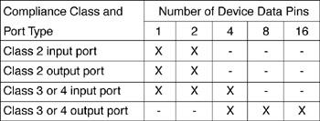
words, does the generation of the debugging information affect the real-time operation of the processor? With a single IEEE 1149.1 port on the processor, the dynamic data flowing out from the port can’t keep up with the processor, and it’s likely that the CPU core would have to periodically stop (stall) to allow the JTAG port to catch up. The Nexus developers anticipated this by defining scalability in terms of features and the I/O hardware necessary to support those features. Thus, by adding additional I/O pins to the processor to add “debugging bandwidth,” dynamic debugging features can be accommodated with minimal intrusion. (However, “minimal” is a loaded word. What is acceptable for one user might cause unpredictable results in another user’s target system.) Figure 7.8 shows this auxiliary I/O port as a schematic representation. Figure 7.11 shows the number of dedicated I/O pins that are necessary for each compliance class. Notice that as many as 16 pins might be necessary for full compliance at Class 4.
Figure 7.11: I/O pins.
Note
The decision to add extra pins to an embedded processor package is not a simple one. Pins are valuable commodities in terms of chip area and package costs.
Nexus port I/O pin requirements.
The driving force to create the Nexus 5001 standard came from the automobile industry, but the standard is not limited to automotive applications. The original working group of five companies were heavily involved in supplying semiconductors or development tools to the automotive industry; however, that group has now grown to over 25 semiconductor and development-tool support companies that have products supporting a wide range of industrial applications of embedded processors. At the same time, several prominent semiconductor manufacturers are not members of the Nexus 5001 group. These companies might choose to remain outside of the standards group because they view their on-chip debug circuitry as a “market differentiator” for them, as well as a competitive advantage.
Summary
The designers of the Nexus standard did several key things correctly. From a technical point of view, this should make the adoption of the standard fairly straightforward. Eventually, members of the Nexus 5001 group will be able to access suggested interface tool designs, representative implementations in Verilog or VHDL, and a standard set of software APIs.
Nexus is a good thing for the industry and will enable both silicon developers and tool developers to bring better debug systems to the market. This, in turn, will help their common customers bring products to market in a timely manner. As former Hewlett-Packard CEO John Young once said, “Standards by themselves are not particularly interesting, but they allow you to do very interesting things.”
Chapter 8: The ICE — An Integrated
Solution
Overview
Chapter 6 introduced the three key capabilities necessary to hardware/software (HW/SW) integration:
Microprocessor run control
Memory substitution
Real-time trace
So far, you’ve learned how to address these capabilities using separate tools, namely a debugging kernel, a ROM emulator, and a logic analyzer. In this chapter, you’ll see what happens when you design a tool system that addresses these needs in a more integrated fashion.
Traditionally, an in-circuit emulator (ICE) is a single-test instrument that integrates all these functions and more. (Modern on-chip debugging support has changed this somewhat, as the later sidebar “Distributed Emulators” explains.) Emulators are the premier tools for HW/SW integration. An emulator’s close coupling of run control, memory substitution, and trace facilities generates a synergism that significantly increases the power of each component.
Even so, the ICE is widely underused. Only about one-third of the embedded system designers, principally firmware developers, use ICE tools. Hopefully, after reading this and the next chapter, you’ll appreciate how important the ICE is to HW/SW integration.
Note
In the language of embedded systems, a firmware developer is someone who writes the low-level driver code that interfaces the software directly to the hardware. Because the ICE has been primarily designated as a HW/SW integration tool, firmware designers have been the people most closely associated with it.
Bullet-Proof Run Control
In the most general case, an ICE uses a debug kernel for run-time control but with a difference that eliminates dependence on the target’s untested memory/processor interface. Instead of relying on the target’s processor and memory, the ICE supplies its own processor and memory. A cable or special connector (see the “Making the Connection” sidebar on page 170) allows the ICE processor to substitute for the target’s processor.
The target program remains in the target memory, but the debug kernel is hosted in the ICE memory. When in normal run mode, the ICE processor reads instructions from the target memory; however, when the debug kernel needs control, the ICE switches to its own local memory. This arrangement ensures that the ICE can maintain run control, even if the target memory is faulty, and also protects the debug kernel from being damaged by bugs in the target.
Figure 8.1 shows a straightforward, generic implementation. The key blocks are labeled:
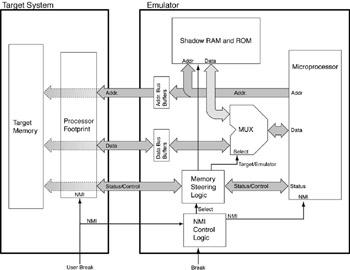
Figure 8.1: General emulator design.
Schematic representation of the architecture of a run control system for a general emulator design.
NMI control logic
Memory steering logic
Shadow ROM and RAM
When the user or emulator decides to stop processing the user’s code and enter the debugger, the NMI signal is asserted, and the NMI control logic responds as follows:
The NMI signal from the target system is blocked by the NMI control logic, so that no further NMI-based interrupts are detected by the processor while it’s executing the code in the debug kernel.
The memory steering logic switches off the address and data bus buffers to the target system and enables the emulator’s local, or “shadow,” memory to connect to the processor. In effect, the context switch occurs by swapping the memory space of the processor.
The processor then takes the interrupt vector that directs it into the debugger entry point, now located in the shadow ROM.
Thus, with this generic emulation system, the only requirement for processor debug support is that the processor has an external NMI capability.
Note
Most processors have a processor input pin called a non-maskable interrupt (NMI). This interrupt signal cannot be ignored (masked) by the processor. It differs from a RESET signal in that the context of the processor can be saved with an NMI but is lost with a RESET. What they have in common is that when either is asserted, the processor must respond to it. In embedded systems, the NMI signal is reserved for catastrophic events, such as a watchdog timer time out or imminent power failure.
Why Emulators Aren’t Used More
In many labs, the entire lab has only one emulator. It sits on a mobile cart and has a long, thin wooden pole attached to it. On the top of the pole is a blaze orange, triangular flag that some engineer purchased in a bike shop for his kid’s bike a few
years ago. Whenever a gnarly problem arises, someone looks for the flag and grabs the emulator. Next, they try to find Joe or Susan — the one or two engineers in the place who actually know how to use it — and hope they can find and fix the problem. The other engineers have been playing with this bug for a week now, and they’ve finally thrown in the towel and want to bring in the big gun. Up to now, they’ve resisted the urge to get the ICE because they figured it would take them the better part of a morning to get it hooked up and running. They always had one other quick-and-dirty test to try that would only take 20 minutes or so. This goes on for a few days until the call goes out to send in the cavalry.
It isn’t always that bad. But I’ve heard that exact scenario enough times and seen enough of those flags to know that I’m on to something. What are they really saying?
Emulators are hard to use. (They certainly can be.)
Emulators are too fragile. (There is also some truth to this but not universally.)
Emulators are too expensive. (Compared to what? What did the lost weeks cost in terms of engineering expenses and time-to-market?)
Emulators won’t run in my target system. (This is rarely true but is an excuse that usually covers up all kinds of system design flaws.)
Emulators don’t fit in my process.
I’ve been getting by without it, and, now that I really do need it, my development process presents a much too closed environment for the ICE to be used effectively. (This can certainly be the case.)
Because of these prevailing perceptions, for many embedded systems developers, the ICE becomes the tool of last resort, rather than an integral part of the tool suite. Unfortunately, that attitude just perpetuates a self-fulfilling prophecy: The ICE isn’t used because it’s too hard to use, which means it will never be under stood well enough to make it easy to use.
Real-Time Trace
After the generic emulator has been attached to the target, acquiring realtime trace information is almost trivial. The emulator already has connections to the necessary address, data, and status busses. To add real-time trace, you just piggy-back a logic analyzer onto the same connection. Thus, without too much additional complexity, you can use the same target system connection that you used for the logic analyzer to concentrate both run control and trace in one target connection instead of in two.
With your new emulation/trace tool, you can control the processor and observe its behavior in real time. Wait, there’s more. Remember that logic analyzers have all this complex circuitry to detect when to begin capturing a trace. Why not use this trigger signal for more than just starting and stopping the trace? Why not also connect it to the NMI control logic so that you can cause the processor to stop program execution and enter the debug monitor program exactly at the place in the code where the event of interest occurs?
Figure 8.2 shows this schematically. The logic analyzer has been added to show how the system functions. The address, data, and status busses are connected to the trace memory and to the trigger system. The trigger system determines when the trace memory should start capturing a trace and when it should stop capturing a trace. It also connects to the NMI control logic block so that you can define
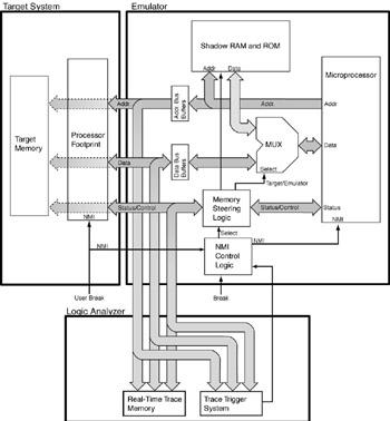
trigger conditions that function independently of the trace system. These other trigger conditions control when the processor stops executing user code and enters the debug kernel (also called the monitor program).
Figure 8.2: Emulation control system.
Block diagram of the core of an emulation control system with real-time trace.
Making the Connection
The emulator’s steering circuitry must be interposed between the pins of the processor and the target system. This can be done in one of two ways:
Remove the target microprocessor from the target (unplug it from its socket)
Disable it in a way that all the pins become open-circuited as far as the target system is concerned (called tri-stated)
If the Target Can Be Socketed Easily
If the footprint of the socket matches the footprint of the microprocessor, it’s sim ple to replace the microprocessor with the appropriate socket and then plug the replacement system into the socket. Of course, the replacement “emulator” must also have some kind of communication port on the board so you can communi cate with your emulation debug kernel, but this is easy to implement. Thus, you can easily add a simple RS232 port to this board and connect the interrupt output signal from the port to the NMI control logic of your emulation circuitry. When a new character is received at the serial port, the NMI is asserted, and you’re into the debug kernel.
If the Target Can’t Be Socketed Easily
Some processors have a dedicated input pin that, when asserted, turns the chip completely off. You can plug the replacement chip (with the emulator signals) into the target system as an overlay. You can do this several wayssome ways are easy, some are not so easy, some are costly, and some are fragile. For example, suppose the target processor is a surface-mounted part with 300 extremely deli cate pins mounted around its periphery. This is typical of what you might expect to find today. If the target system has room, the hardware designers might be able to place some high-density sockets on the target PC board so that each pin of the socket intercepts one of the I/O pins of the target processor. Two or three highdensity sockets easily can cover the 300 pins of the target processor. If you get the mechanical design just right, you should be able to plug the connectors on the emulator board into the matching sockets of the target system.
If the target processor has a “disable everything” pin, you can turn it off. If it doesn’t, you must remove the processor from the target and depend on the emula tion processor, mounted on the generic emulation board, to become the target processor. You probably won’t have the luxury of sockets on the target system, so go to plan B.
In this situation, you need to find a manufacturer of specialized connection devices (such as Ironwood Electronics Corporation at www.ironwoodelectron ics.com or Emulation Technology, Inc., at www.emulation.com) so you can solder an interface connector to the 300-pin footprint on your target printed circuit board and provide a mating socket into which ou can plug your emulator. This is shown schematically in Figure 8.3, in which a mechanical adapter can be soldered to the target system PC board to replace the embedded microprocessor that you are trying to emulate/control.
With this socket adapter mounted to the PC board, you can plug in the target pro cessor (by mounting it to a small PC board with an SMT footprint on the top side and mating PGA pins on the bottom), or you can plug in your emulator. Adapters such as this cost anywhere from $1 per pin to $5 per pin, so one very fragile adapter might set you back $1,000. Also, because these sockets add some addi tional length to the electrical interconnections of the target system, some distor tion of the waveforms might occur at high bus rates. How this impacts your target system is generally impossible to predict in advance.
Another advantage of this technique is that it’s generally usable with many minia ture and crowded target systems. That’s not to say that it’s universal because some perverse mechanical designs are out there that absolutely defy physical access, but, at least in this situation, it’s not taking up any more space at the board-level than the actual footprint of the microprocessor itself.
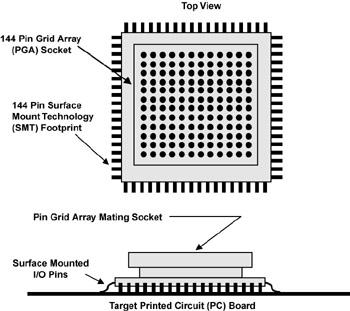
Figure 8.3: Mechanical adapter.
An adapter for converting a surface-mounted package into a pin-grid array style socket.
Hardware Breakpoints
Now you can let the trigger system of the logic analyzer take over some of the functionality that was previously supplied by the debug kernel. You can set a breakpoint, or a complex break condition, in the trigger system and let it signal the breakpoint in real time as the program executes at full speed.
Note
Many discrete logic analyzers have the capability to output a trigger pulse. Often, you can use this pulse as an input to your BDM or JTAG interface to force the debug core to stop execution. However, a large number of instructions might get executed after the break condition occurs (called skew), so, if you really want to stop on a dime, this method forces some compromises.
This looks pretty good. Using the combination of the run control functionality of a debugger with the capability to set a breakpoint lets the user halt execution of the code without slowing the processor down the way a real debugger would. Also, you can still set your breakpoint even if the code you are running is located in ROM. As a bonus, the trace capability of the logic analyzer allows you to see what’s happening, or what’s happened, in real time. If you have an ISR that comes on 0.000000001% of the time, the logic analyzer can capture it when it happens and show you what it’s doing.
So what’s a good trigger signal?
How you set up the trigger signal depends upon what you’re looking for. Let’s say that you’re interested in debugging a very short and infrequent ISR. In this exam ple system, the interrupt causes the processor to read automatically from memory
location 0x00000078 and use the data valued stored there as the memory loca tion of the first instruction of the ISR. This is normally referred to as an exception vector. The vector in this case is a term used for an indirect memory access. In this example, we could set the trigger to be asserted when the processor does a read from memory location 0x00000078. Thus, our trigger condition in this situation is a specific address and a processor-read cycle. In this example, we don’t care what the data value happens to be, so we’ll only assert the trigger on the address and status bits. Also, we want the system to begin recording states after the trig ger occurs and stop recording before we overwrite the states we recorded begin ning from the trigger point. Thus, no matter how infrequently the ISR occurs or how short it is, the logic analyzer will continue recording and overwriting until the trigger condition is met, and the logic analyzer captures a trace buffer full of states.
Let’s consider a different situation. Suppose that the exception vector is caused by a program fault, such as an illegal op-code, but when the exception processing occurs, it also seems to be failing. In this case, you would want to set the trigger point so that the trigger point occurs in the middle of the trace buffer. In this way, you can see all of the states of the system leading up to the failure and then see what the processor executed once the exception vector is taken. Most logic ana lyzers allow you to set the trigger event to occur anywhere in the buffer memory.
Thus, you can record all the states that occurred leading up to the trigger event, all of the states following the trigger event, and everything in between.
Our previous example shows that we can easily specify an address as a trigger condition. As a C or C++ programmer, it’s usually not convenient to have to find out where the addresses of variables are located. The compiler takes care of those details so we don’t have to. Therefore, just as with a source-level debugger, we should be able to use the same logic analyzer soft ware that provides us with sym bolic trace information to allow us to create trigger conditions without having to know the low-level details. Thus, if I write a simple function foo():
int foo( int, bar)
{
int embedded = 15;
bar++;
return embedded+bar ;
}
Let’s assume that for some very strange reason the function that calls foo() some times gets an erroneous return value back. When you single-stepped your pro gram on the host, it worked just fine. You suspect that an ISR is overwriting your local variable on the stack. You could look up the symbol table and link map and figure out where the function is located, or, if your LA is suitably appointed, you could tell it to trigger on foo() and have the software figure out where foo() hap pens to be in memory.
Overlay Memory
Even though triggered breakpoints work on code located in ROM, you still need some kind of substitution memory, if for no other reason than to speed up the edit–compile–link–load–debug cycle. Chapter 6 covered the ROM emulator, a device that plugs into the ROM sockets and replaces the ROM, while providing an easy method of downloading code through an Ethernet or serial port. You could do that here as well. This is called substitution memory because it’s used to substitute one form of memory, RAM, for another form, ROM. The substitution memory lives in the same space as the ROM that would normally be plugged into the socket. Today, most emulators don’t use substitution memory, although they certainly could. Because the emulator already has steering logic to determine which memory space from which it grabs the next instruction (the target memory or the shadow memory as shown previously in Figure 8.2), it wouldn’t be much more complicated to design an emulation memory system that could overlay the target memory system. Thus, for certain memory operations, you could go to the target system to read or write memory. For other operations, such as fetching instructions, you could activate this other memory that is connected to the emulator and is presumably easy to download to with new instructions or data. This other type of memory is called overlay memory because it can cover broad areas of the processor’s address space, rather than look at the target system through the ROM socket.
Overlay memory is extremely useful. In fact, it’s much more useful than substitution memory. Overlay memory uses the same trick that is used with shadow memory. On a bus cycle-by-bus cycle basis, fast buffers and steering logic are used to decide to which block of memory the processor actually connects. The block of memory can exist on the target, in shadow memory, or in overlay memory. In a way, the memory steering logic functions much like an on-chip Memory Management Unit (MMU). The circuitry maps the physical address being output by the processor to various external memories.
Figure 8.4 shows how you can set up an overlay memory system. Suppose your processor has a 32-bit address bus and the smallest block of overlay memory you can map in or out is 16KB. Also, assume that you have a total of 1MB of emulation, or overlay memory. If you divide this memory into 16KB chunks, you have a total of 64 16KB blocks that can be used to overlay or to replace any one of the 256KB blocks in the target memory space. Assuming you have some magical way of programming the memorymapper RAM, you can then program each 18-bit data value in the mapper RAM to translate the 18-bit input address from the target microprocessor to another value on the output. One address goes in; another goes out as data. If you program every memory location in the mapper RAM with the corresponding address value, the mapper has no apparent effect, other than using up some valuable time that might otherwise be available to the target system’s memory.