

Ш-V Semiconductor Integrated Cifcuits
III-V semiconductors attract the attention of scientists and manufacturers working in the field of microelectronics. This interest is based upon the ability of these materials to satisfy a wide variety of needs.
Technological applications include high speed processing, communications, sensing and imagining, and many others. Integrated circuits with various combinations of MESFET, JFET, bipolar, Gunn, Schottky diode, laser diode, optical detector, light guide, acoustic wave, and other assorted functions are being explored, developed and utilized.
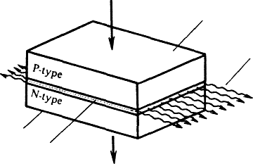
One of the first large-scale applications of Ш-V semiconductors was light-emitting diodes (LEDs) which are two terminal devices that emit light when a forward-bias current is passed through a p-n junction. An energy state and device construction is given in Fig. 3.
current flow
contact
radiations
contact
active region
current flow
Рис.3
When an electron in the conduction band combines with a hole in the valence band, the energy is emitted as a photon and light is produced. Of course, non-radiative combination processes and light re-absorption must be minimized for high efficiency. To emit light visible to the human eye, a band gap near 2 eV is necessary to provide the proper photon energy, which precludes use of the semiconductors except GaP, which produces red-green light.
At the beginning of the 1970’s, the GaAs MESFET device was developed for use in circuits such as microwave amplifiers operating in the frequencies range from about 2 to 12 GHz. The device is fabricated on a base of single-crystal semi-insulating GaAs. A GaAs film containing a closely-controlled concentration of n-type dopant atoms is epitaxially deposited on the GaAs wafer. The devices are completed by etching "mesas" or islands to electrically isolate the device and by adding low resistance contacts and a gate electrode. The gate length is typically 1 µm.
The first integration of GaAs MESFET transistors into logic gates was done in 1974. These gates have been integrated into gated flip-flop integrated circuits and used for prescalers and time-interval measurements. These GaAs integrated circuits operate at substantially higher speeds than silicon ICs because of a combination of higher transconductance due to higher electron mobility, and lower parasitic capacitance due to higher substrate resistivity. The higher substrate resistivity in GaAs is a result of its larger bandgap. Semi-insulating GaAs material naturally provides device-to-device electrical isolation.
Digital capability in GaAs has passed from the SSI (small-scale integration, ~ 10 gates) realm into the MSI (medium-scale integration, ~ 100 gates), and is headed for LSI (large-scale integration, ~ 1000 gates). Fabrication of an 8 x 8 bit parallel multiplier (1008 gates fabricated from approximately 6000 transistors and diodes) has been recently reported, which is the most complex GaAs integrated circuit reported to date.
GaAs IC technology is being developed to meet important system needs. Advanced systems are faced with challenges which require significant advances in the rate of real-time signal. An attractive objective is to convert analog microwave signals to digital format in a high-speed A/D converter as close as possible to the microwave receiver front, and then to process the data digitally. The bandwidth which can be achieved in GaAs should be capable of permitting digital processing of microwave signals including A/D conversion to become a reality.
Учитесь говорить.
3.26. На основе прочитанных текстов и ваших знаний по специальности подготовьте сообщения на английском языке по следующим темам:
Рис. 4
1. Технология полупроводниковых приборов и интегральных схем. 2. Новые материалы и новые технологии в производстве ИС, БИС, СБИС.
3.27. Изучите схему технологических процессов (Рис. 4) и составьте аналогичную схему на английском языке.
3.28. Сравните информацию, изложенную в тексте, со схемой планарного процесса производства кремниевого р-п-р транзистора. Составьте аналогичную схему на английском языке.
3.29. Прочитайте стихотворение Chip Fabrication, написанное одним из редакторов журнала IEЕЕ Transactions on Electron Devices. Дайте подстрочный (или стихотворный) перевод.