

- •Preface
- •Imaging Microscopic Features
- •Measuring the Crystal Structure
- •References
- •Contents
- •1.4 Simulating the Effects of Elastic Scattering: Monte Carlo Calculations
- •What Are the Main Features of the Beam Electron Interaction Volume?
- •How Does the Interaction Volume Change with Composition?
- •How Does the Interaction Volume Change with Incident Beam Energy?
- •How Does the Interaction Volume Change with Specimen Tilt?
- •1.5 A Range Equation To Estimate the Size of the Interaction Volume
- •References
- •2: Backscattered Electrons
- •2.1 Origin
- •2.2.1 BSE Response to Specimen Composition (η vs. Atomic Number, Z)
- •SEM Image Contrast with BSE: “Atomic Number Contrast”
- •SEM Image Contrast: “BSE Topographic Contrast—Number Effects”
- •2.2.3 Angular Distribution of Backscattering
- •Beam Incident at an Acute Angle to the Specimen Surface (Specimen Tilt > 0°)
- •SEM Image Contrast: “BSE Topographic Contrast—Trajectory Effects”
- •2.2.4 Spatial Distribution of Backscattering
- •Depth Distribution of Backscattering
- •Radial Distribution of Backscattered Electrons
- •2.3 Summary
- •References
- •3: Secondary Electrons
- •3.1 Origin
- •3.2 Energy Distribution
- •3.3 Escape Depth of Secondary Electrons
- •3.8 Spatial Characteristics of Secondary Electrons
- •References
- •4: X-Rays
- •4.1 Overview
- •4.2 Characteristic X-Rays
- •4.2.1 Origin
- •4.2.2 Fluorescence Yield
- •4.2.3 X-Ray Families
- •4.2.4 X-Ray Nomenclature
- •4.2.6 Characteristic X-Ray Intensity
- •Isolated Atoms
- •X-Ray Production in Thin Foils
- •X-Ray Intensity Emitted from Thick, Solid Specimens
- •4.3 X-Ray Continuum (bremsstrahlung)
- •4.3.1 X-Ray Continuum Intensity
- •4.3.3 Range of X-ray Production
- •4.4 X-Ray Absorption
- •4.5 X-Ray Fluorescence
- •References
- •5.1 Electron Beam Parameters
- •5.2 Electron Optical Parameters
- •5.2.1 Beam Energy
- •Landing Energy
- •5.2.2 Beam Diameter
- •5.2.3 Beam Current
- •5.2.4 Beam Current Density
- •5.2.5 Beam Convergence Angle, α
- •5.2.6 Beam Solid Angle
- •5.2.7 Electron Optical Brightness, β
- •Brightness Equation
- •5.2.8 Focus
- •Astigmatism
- •5.3 SEM Imaging Modes
- •5.3.1 High Depth-of-Field Mode
- •5.3.2 High-Current Mode
- •5.3.3 Resolution Mode
- •5.3.4 Low-Voltage Mode
- •5.4 Electron Detectors
- •5.4.1 Important Properties of BSE and SE for Detector Design and Operation
- •Abundance
- •Angular Distribution
- •Kinetic Energy Response
- •5.4.2 Detector Characteristics
- •Angular Measures for Electron Detectors
- •Elevation (Take-Off) Angle, ψ, and Azimuthal Angle, ζ
- •Solid Angle, Ω
- •Energy Response
- •Bandwidth
- •5.4.3 Common Types of Electron Detectors
- •Backscattered Electrons
- •Passive Detectors
- •Scintillation Detectors
- •Semiconductor BSE Detectors
- •5.4.4 Secondary Electron Detectors
- •Everhart–Thornley Detector
- •Through-the-Lens (TTL) Electron Detectors
- •TTL SE Detector
- •TTL BSE Detector
- •Measuring the DQE: BSE Semiconductor Detector
- •References
- •6: Image Formation
- •6.1 Image Construction by Scanning Action
- •6.2 Magnification
- •6.3 Making Dimensional Measurements With the SEM: How Big Is That Feature?
- •Using a Calibrated Structure in ImageJ-Fiji
- •6.4 Image Defects
- •6.4.1 Projection Distortion (Foreshortening)
- •6.4.2 Image Defocusing (Blurring)
- •6.5 Making Measurements on Surfaces With Arbitrary Topography: Stereomicroscopy
- •6.5.1 Qualitative Stereomicroscopy
- •Fixed beam, Specimen Position Altered
- •Fixed Specimen, Beam Incidence Angle Changed
- •6.5.2 Quantitative Stereomicroscopy
- •Measuring a Simple Vertical Displacement
- •References
- •7: SEM Image Interpretation
- •7.1 Information in SEM Images
- •7.2.2 Calculating Atomic Number Contrast
- •Establishing a Robust Light-Optical Analogy
- •Getting It Wrong: Breaking the Light-Optical Analogy of the Everhart–Thornley (Positive Bias) Detector
- •Deconstructing the SEM/E–T Image of Topography
- •SUM Mode (A + B)
- •DIFFERENCE Mode (A−B)
- •References
- •References
- •9: Image Defects
- •9.1 Charging
- •9.1.1 What Is Specimen Charging?
- •9.1.3 Techniques to Control Charging Artifacts (High Vacuum Instruments)
- •Observing Uncoated Specimens
- •Coating an Insulating Specimen for Charge Dissipation
- •Choosing the Coating for Imaging Morphology
- •9.2 Radiation Damage
- •9.3 Contamination
- •References
- •10: High Resolution Imaging
- •10.2 Instrumentation Considerations
- •10.4.1 SE Range Effects Produce Bright Edges (Isolated Edges)
- •10.4.4 Too Much of a Good Thing: The Bright Edge Effect Hinders Locating the True Position of an Edge for Critical Dimension Metrology
- •10.5.1 Beam Energy Strategies
- •Low Beam Energy Strategy
- •High Beam Energy Strategy
- •Making More SE1: Apply a Thin High-δ Metal Coating
- •Making Fewer BSEs, SE2, and SE3 by Eliminating Bulk Scattering From the Substrate
- •10.6 Factors That Hinder Achieving High Resolution
- •10.6.2 Pathological Specimen Behavior
- •Contamination
- •Instabilities
- •References
- •11: Low Beam Energy SEM
- •11.3 Selecting the Beam Energy to Control the Spatial Sampling of Imaging Signals
- •11.3.1 Low Beam Energy for High Lateral Resolution SEM
- •11.3.2 Low Beam Energy for High Depth Resolution SEM
- •11.3.3 Extremely Low Beam Energy Imaging
- •References
- •12.1.1 Stable Electron Source Operation
- •12.1.2 Maintaining Beam Integrity
- •12.1.4 Minimizing Contamination
- •12.3.1 Control of Specimen Charging
- •12.5 VPSEM Image Resolution
- •References
- •13: ImageJ and Fiji
- •13.1 The ImageJ Universe
- •13.2 Fiji
- •13.3 Plugins
- •13.4 Where to Learn More
- •References
- •14: SEM Imaging Checklist
- •14.1.1 Conducting or Semiconducting Specimens
- •14.1.2 Insulating Specimens
- •14.2 Electron Signals Available
- •14.2.1 Beam Electron Range
- •14.2.2 Backscattered Electrons
- •14.2.3 Secondary Electrons
- •14.3 Selecting the Electron Detector
- •14.3.2 Backscattered Electron Detectors
- •14.3.3 “Through-the-Lens” Detectors
- •14.4 Selecting the Beam Energy for SEM Imaging
- •14.4.4 High Resolution SEM Imaging
- •Strategy 1
- •Strategy 2
- •14.5 Selecting the Beam Current
- •14.5.1 High Resolution Imaging
- •14.5.2 Low Contrast Features Require High Beam Current and/or Long Frame Time to Establish Visibility
- •14.6 Image Presentation
- •14.6.1 “Live” Display Adjustments
- •14.6.2 Post-Collection Processing
- •14.7 Image Interpretation
- •14.7.1 Observer’s Point of View
- •14.7.3 Contrast Encoding
- •14.8.1 VPSEM Advantages
- •14.8.2 VPSEM Disadvantages
- •15: SEM Case Studies
- •15.1 Case Study: How High Is That Feature Relative to Another?
- •15.2 Revealing Shallow Surface Relief
- •16.1.2 Minor Artifacts: The Si-Escape Peak
- •16.1.3 Minor Artifacts: Coincidence Peaks
- •16.1.4 Minor Artifacts: Si Absorption Edge and Si Internal Fluorescence Peak
- •16.2 “Best Practices” for Electron-Excited EDS Operation
- •16.2.1 Operation of the EDS System
- •Choosing the EDS Time Constant (Resolution and Throughput)
- •Choosing the Solid Angle of the EDS
- •Selecting a Beam Current for an Acceptable Level of System Dead-Time
- •16.3.1 Detector Geometry
- •16.3.2 Process Time
- •16.3.3 Optimal Working Distance
- •16.3.4 Detector Orientation
- •16.3.5 Count Rate Linearity
- •16.3.6 Energy Calibration Linearity
- •16.3.7 Other Items
- •16.3.8 Setting Up a Quality Control Program
- •Using the QC Tools Within DTSA-II
- •Creating a QC Project
- •Linearity of Output Count Rate with Live-Time Dose
- •Resolution and Peak Position Stability with Count Rate
- •Solid Angle for Low X-ray Flux
- •Maximizing Throughput at Moderate Resolution
- •References
- •17: DTSA-II EDS Software
- •17.1 Getting Started With NIST DTSA-II
- •17.1.1 Motivation
- •17.1.2 Platform
- •17.1.3 Overview
- •17.1.4 Design
- •Simulation
- •Quantification
- •Experiment Design
- •Modeled Detectors (. Fig. 17.1)
- •Window Type (. Fig. 17.2)
- •The Optimal Working Distance (. Figs. 17.3 and 17.4)
- •Elevation Angle
- •Sample-to-Detector Distance
- •Detector Area
- •Crystal Thickness
- •Number of Channels, Energy Scale, and Zero Offset
- •Resolution at Mn Kα (Approximate)
- •Azimuthal Angle
- •Gold Layer, Aluminum Layer, Nickel Layer
- •Dead Layer
- •Zero Strobe Discriminator (. Figs. 17.7 and 17.8)
- •Material Editor Dialog (. Figs. 17.9, 17.10, 17.11, 17.12, 17.13, and 17.14)
- •17.2.1 Introduction
- •17.2.2 Monte Carlo Simulation
- •17.2.4 Optional Tables
- •References
- •18: Qualitative Elemental Analysis by Energy Dispersive X-Ray Spectrometry
- •18.1 Quality Assurance Issues for Qualitative Analysis: EDS Calibration
- •18.2 Principles of Qualitative EDS Analysis
- •Exciting Characteristic X-Rays
- •Fluorescence Yield
- •X-ray Absorption
- •Si Escape Peak
- •Coincidence Peaks
- •18.3 Performing Manual Qualitative Analysis
- •Beam Energy
- •Choosing the EDS Resolution (Detector Time Constant)
- •Obtaining Adequate Counts
- •18.4.1 Employ the Available Software Tools
- •18.4.3 Lower Photon Energy Region
- •18.4.5 Checking Your Work
- •18.5 A Worked Example of Manual Peak Identification
- •References
- •19.1 What Is a k-ratio?
- •19.3 Sets of k-ratios
- •19.5 The Analytical Total
- •19.6 Normalization
- •19.7.1 Oxygen by Assumed Stoichiometry
- •19.7.3 Element by Difference
- •19.8 Ways of Reporting Composition
- •19.8.1 Mass Fraction
- •19.8.2 Atomic Fraction
- •19.8.3 Stoichiometry
- •19.8.4 Oxide Fractions
- •Example Calculations
- •19.9 The Accuracy of Quantitative Electron-Excited X-ray Microanalysis
- •19.9.1 Standards-Based k-ratio Protocol
- •19.9.2 “Standardless Analysis”
- •19.10 Appendix
- •19.10.1 The Need for Matrix Corrections To Achieve Quantitative Analysis
- •19.10.2 The Physical Origin of Matrix Effects
- •19.10.3 ZAF Factors in Microanalysis
- •X-ray Generation With Depth, φ(ρz)
- •X-ray Absorption Effect, A
- •X-ray Fluorescence, F
- •References
- •20.2 Instrumentation Requirements
- •20.2.1 Choosing the EDS Parameters
- •EDS Spectrum Channel Energy Width and Spectrum Energy Span
- •EDS Time Constant (Resolution and Throughput)
- •EDS Calibration
- •EDS Solid Angle
- •20.2.2 Choosing the Beam Energy, E0
- •20.2.3 Measuring the Beam Current
- •20.2.4 Choosing the Beam Current
- •Optimizing Analysis Strategy
- •20.3.4 Ba-Ti Interference in BaTiSi3O9
- •20.4 The Need for an Iterative Qualitative and Quantitative Analysis Strategy
- •20.4.2 Analysis of a Stainless Steel
- •20.5 Is the Specimen Homogeneous?
- •20.6 Beam-Sensitive Specimens
- •20.6.1 Alkali Element Migration
- •20.6.2 Materials Subject to Mass Loss During Electron Bombardment—the Marshall-Hall Method
- •Thin Section Analysis
- •Bulk Biological and Organic Specimens
- •References
- •21: Trace Analysis by SEM/EDS
- •21.1 Limits of Detection for SEM/EDS Microanalysis
- •21.2.1 Estimating CDL from a Trace or Minor Constituent from Measuring a Known Standard
- •21.2.2 Estimating CDL After Determination of a Minor or Trace Constituent with Severe Peak Interference from a Major Constituent
- •21.3 Measurements of Trace Constituents by Electron-Excited Energy Dispersive X-ray Spectrometry
- •The Inevitable Physics of Remote Excitation Within the Specimen: Secondary Fluorescence Beyond the Electron Interaction Volume
- •Simulation of Long-Range Secondary X-ray Fluorescence
- •NIST DTSA II Simulation: Vertical Interface Between Two Regions of Different Composition in a Flat Bulk Target
- •NIST DTSA II Simulation: Cubic Particle Embedded in a Bulk Matrix
- •21.5 Summary
- •References
- •22.1.2 Low Beam Energy Analysis Range
- •22.2 Advantage of Low Beam Energy X-Ray Microanalysis
- •22.2.1 Improved Spatial Resolution
- •22.3 Challenges and Limitations of Low Beam Energy X-Ray Microanalysis
- •22.3.1 Reduced Access to Elements
- •22.3.3 At Low Beam Energy, Almost Everything Is Found To Be Layered
- •Analysis of Surface Contamination
- •References
- •23: Analysis of Specimens with Special Geometry: Irregular Bulk Objects and Particles
- •23.2.1 No Chemical Etching
- •23.3 Consequences of Attempting Analysis of Bulk Materials With Rough Surfaces
- •23.4.1 The Raw Analytical Total
- •23.4.2 The Shape of the EDS Spectrum
- •23.5 Best Practices for Analysis of Rough Bulk Samples
- •23.6 Particle Analysis
- •Particle Sample Preparation: Bulk Substrate
- •The Importance of Beam Placement
- •Overscanning
- •“Particle Mass Effect”
- •“Particle Absorption Effect”
- •The Analytical Total Reveals the Impact of Particle Effects
- •Does Overscanning Help?
- •23.6.6 Peak-to-Background (P/B) Method
- •Specimen Geometry Severely Affects the k-ratio, but Not the P/B
- •Using the P/B Correspondence
- •23.7 Summary
- •References
- •24: Compositional Mapping
- •24.2 X-Ray Spectrum Imaging
- •24.2.1 Utilizing XSI Datacubes
- •24.2.2 Derived Spectra
- •SUM Spectrum
- •MAXIMUM PIXEL Spectrum
- •24.3 Quantitative Compositional Mapping
- •24.4 Strategy for XSI Elemental Mapping Data Collection
- •24.4.1 Choosing the EDS Dead-Time
- •24.4.2 Choosing the Pixel Density
- •24.4.3 Choosing the Pixel Dwell Time
- •“Flash Mapping”
- •High Count Mapping
- •References
- •25.1 Gas Scattering Effects in the VPSEM
- •25.1.1 Why Doesn’t the EDS Collimator Exclude the Remote Skirt X-Rays?
- •25.2 What Can Be Done To Minimize gas Scattering in VPSEM?
- •25.2.2 Favorable Sample Characteristics
- •Particle Analysis
- •25.2.3 Unfavorable Sample Characteristics
- •References
- •26.1 Instrumentation
- •26.1.2 EDS Detector
- •26.1.3 Probe Current Measurement Device
- •Direct Measurement: Using a Faraday Cup and Picoammeter
- •A Faraday Cup
- •Electrically Isolated Stage
- •Indirect Measurement: Using a Calibration Spectrum
- •26.1.4 Conductive Coating
- •26.2 Sample Preparation
- •26.2.1 Standard Materials
- •26.2.2 Peak Reference Materials
- •26.3 Initial Set-Up
- •26.3.1 Calibrating the EDS Detector
- •Selecting a Pulse Process Time Constant
- •Energy Calibration
- •Quality Control
- •Sample Orientation
- •Detector Position
- •Probe Current
- •26.4 Collecting Data
- •26.4.1 Exploratory Spectrum
- •26.4.2 Experiment Optimization
- •26.4.3 Selecting Standards
- •26.4.4 Reference Spectra
- •26.4.5 Collecting Standards
- •26.4.6 Collecting Peak-Fitting References
- •26.5 Data Analysis
- •26.5.2 Quantification
- •26.6 Quality Check
- •Reference
- •27.2 Case Study: Aluminum Wire Failures in Residential Wiring
- •References
- •28: Cathodoluminescence
- •28.1 Origin
- •28.2 Measuring Cathodoluminescence
- •28.3 Applications of CL
- •28.3.1 Geology
- •Carbonado Diamond
- •Ancient Impact Zircons
- •28.3.2 Materials Science
- •Semiconductors
- •Lead-Acid Battery Plate Reactions
- •28.3.3 Organic Compounds
- •References
- •29.1.1 Single Crystals
- •29.1.2 Polycrystalline Materials
- •29.1.3 Conditions for Detecting Electron Channeling Contrast
- •Specimen Preparation
- •Instrument Conditions
- •29.2.1 Origin of EBSD Patterns
- •29.2.2 Cameras for EBSD Pattern Detection
- •29.2.3 EBSD Spatial Resolution
- •29.2.5 Steps in Typical EBSD Measurements
- •Sample Preparation for EBSD
- •Align Sample in the SEM
- •Check for EBSD Patterns
- •Adjust SEM and Select EBSD Map Parameters
- •Run the Automated Map
- •29.2.6 Display of the Acquired Data
- •29.2.7 Other Map Components
- •29.2.10 Application Example
- •Application of EBSD To Understand Meteorite Formation
- •29.2.11 Summary
- •Specimen Considerations
- •EBSD Detector
- •Selection of Candidate Crystallographic Phases
- •Microscope Operating Conditions and Pattern Optimization
- •Selection of EBSD Acquisition Parameters
- •Collect the Orientation Map
- •References
- •30.1 Introduction
- •30.2 Ion–Solid Interactions
- •30.3 Focused Ion Beam Systems
- •30.5 Preparation of Samples for SEM
- •30.5.1 Cross-Section Preparation
- •30.5.2 FIB Sample Preparation for 3D Techniques and Imaging
- •30.6 Summary
- •References
- •31: Ion Beam Microscopy
- •31.1 What Is So Useful About Ions?
- •31.2 Generating Ion Beams
- •31.3 Signal Generation in the HIM
- •31.5 Patterning with Ion Beams
- •31.7 Chemical Microanalysis with Ion Beams
- •References
- •Appendix
- •A Database of Electron–Solid Interactions
- •A Database of Electron–Solid Interactions
- •Introduction
- •Backscattered Electrons
- •Secondary Yields
- •Stopping Powers
- •X-ray Ionization Cross Sections
- •Conclusions
- •References
- •Index
- •Reference List
- •Index

20.2 · Instrumentation Requirements
FWHM or more, depending on the choice of time constant. For the particular silicon drift detector (SDD)-EDS and time constant shown in . Fig. 20.1, the broadened EDS peak has a FWHM = 126 eV. The peak width increases (i.e., resolution becomes poorer) as the time constant decreases. The shortest time constant, which gives the highest throughput but the broadest peaks (poorest resolution), is typically chosen for analysis situations where it is important to maximize the total number of X-ray counts per unit of clock (real) time, such as elemental X-ray mapping. For quantitative analysis, better peak resolution is desirable, and thus a longer time constant should be chosen. Whichever time constant strategy is selected, it is important for standardsbased quantitative analysis that this same time constant be used for all measurements of unknowns and standards, especially if archived standards are used.
EDS Calibration
Assigning the proper energy bin for a photon measurement depends on the EDS being calibrated. The vendor for a particular EDS system will have a recommended calibration procedure that should be followed on a regular basis as part of establishing a quality measurement environment, with full documentation of the measurements to establish the on-going calibration record. A typical calibration strategy is to choose a material such as Cu that provides (with E0 ≥ 15 keV) strongly excited peaks in the low photon energy range (Cu L3M5 = 0.93 keV) and the high photon energy range (Cu K-L2,3 = 8.04 keV). Alternatively, some EDS systems that provide a “zero energy reference” signal will use this value with a single
high photon energy peak such as Cu K-L2,3 or Mn K-L2,3 to perform calibration. A good quality assurance practice is
to begin each measurement campaign by measuring a spectrum of Cu (or another element, e.g., Mn, Ni, etc., or a compound, e.g., CuS, FeS2, etc.) under the user-defined conditions. This Cu spectrum can be compared to the Cu spectrum that is stored in the archive of standards to confirm that the current measurement conditions are identical to those used to create the archive. This starting Cu spectrum should always be saved as part of the quality assurance plan.
EDS Solid Angle
The solid angle of collection, Ω, is given by
Ω = A / r2 |
\ |
(20.1) |
|
|
where A is the active area of the detector and r is the distance from the X-ray source on the specimen to the detector. Some
EDS systems are mounted on a retractable arm that enables the analyst to choose the value of r. A consistent and
313 |
|
20 |
|
|
|
reproducible choice must be made for r since this value has such a strong impact on Ω and thus on the number of photons detected per unit of dose.
20.2.2\ Choosing the Beam Energy, E0
The choice of beam energy depends on the particular aspects of the analysis that the analyst wishes to optimize. As a starting point, a useful general analysis strategy is to optimize the excitation of photon energies up to 12 keV by choosing an incident beam energy of 20 keV, which provides sufficient overvoltage (E0/Ec > 1.5) for K-shell (to Br) and L-shell (elements to Bi) for reasonable excitation. The characteristic peaks of X-ray families that occur in the photon energy range from 4 keV to 12 keV are generally sufficiently separated in energy to be resolved by
EDS. When it is important to measure those elements whose characteristic peaks occur below 4 keV, and especially for the low atomic number elements Be, B, C, N, O and F, for which the characteristic peaks occur below 1 keV and suffer high absorption, then analysis with lower beam energy, 10 keV or lower, will be necessary to optimize the results.
20.2.3\ Measuring the Beam Current
The SEM should be equipped for beam current measurement, ideally with an in-column Faraday cup which can be selected periodically during the analysis procedure to determine the beam current. As an alternative, a picoammeter can be installed between the electrically isolated specimen stage and the electrical ground to measure the absorbed (specimen) current that must flow to ground to avoid specimen charging. The specimen current is the difference between the beam current and the loss of charge due to BSE and SE emission, both of which vary with composition. To measure the true beam current, BSE and SE emission must be recaptured, which is accomplished by placing the beam within a Faraday cup, which is constructed as a blind hole in a conducting material (e.g., metal or carbon) covered with a small entrance aperture (e.g., an electron microscope aperture of 50 μm diameter or less). This Faraday cup is then placed at a suitable location on the electrically isolated specimen stage. By locating the beam in the center of the Faraday cup aperture opening, the primary beam electrons as well as all BSEs and SEs generated at the inner surfaces are collected with very little loss through the small aperture, so that the current flowing to the electrical ground is the total incident beam current.
\314 Chapter 20 · Quantitative Analysis: The SEM/EDS Elemental Microanalysis k-ratio Procedure for Bulk Specimens, Step-by-Step
20.2.4\ Choosing the Beam Current
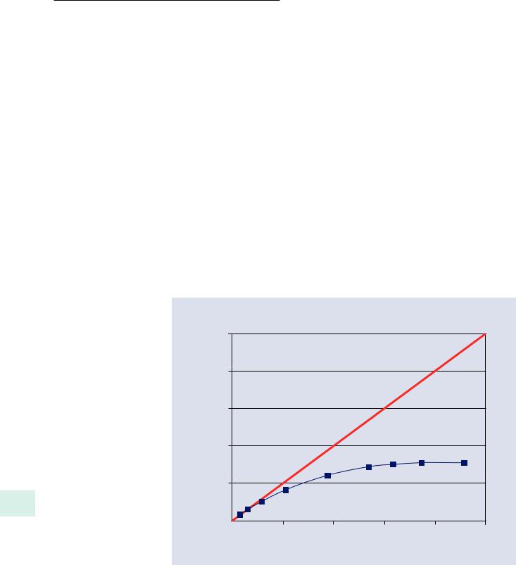
After the analyst has chosen the EDS time constant, the detector solid angle (for a retractable detector), and the beam energy, the beam current should be chosen so as to give a reasonable detector throughput, as expressed by the system dead-time. . Figure 20.2 shows the relationship between the input count rate (ICR) of X-rays that arrive at the detector and the output count rate (OCR) of photons that are actually stored in the measured spectrum. The OCR initially rises linearly with the ICR, but as photons arrive at a progressively greater rate at the detector, photon coincidence begins to occur and the anti-coincidence function begins to reject these coincidence events, reducing the OCR. Eventually a maximum OCR value is reached beyond which the OCR decreases with increasing ICR, eventually falling to zero (“paralyzable dead-time”). A useful measure of the activity state of the EDS detector is the system “dead-time” which is defined as
Dead-time |
( |
% |
) |
( |
ICR − OCR |
) |
|
100 |
|
|
|
|
= |
|
/ ICR |
\ |
(20.2) |
||||
|
|
|
|
|
|
|
|
|
|
A classic strategy with the low throughput Si(Li)-EDS is to select a beam current on a highly excited pure element such as Al or Si that produces a dead-time of 30 % or less. With
SDD-EDS, a more conservative counting strategy is suggested, such that the beam current is chosen so that the dead-time on the most highly excited standard of interest, for example, Al or Si, is less than 10 %. Despite the operation of the anti-coincidence function, SDD-EDS systems typically show evidence of coincidence peaks above a deadtime of 10 % from highly excited parent peaks, as illustrated in . Fig. 20.3, which shows the in-growth of an extensive set of coincidence peaks from several parent peaks. If it is important to measure low intensity X-ray peaks that correspond to minor or trace constituents that occur in spectral regions affected by coincidence peaks, then choosing the low dead-time to minimize coincidence will be an important issue in selecting the general analytical conditions. If there is no interest in measuring X-ray peaks of possible constituents that occur in the region of coincidence peaks, then these regions can be ignored and a counting strategy that involves higher dead-time operation can be used.
Once the analytical conditions (EDS time constant, solid angle, beam energy, and beam current appropriate to the complete suite of standards) have been chosen, these conditions should be used for all standards and unknowns to achieve the basic measurement consistency required for the k-ratio/matrix corrections protocol.
. Fig. 20.2 Output count rate (OCR) vs. input count rate for an SDD-EDS array of four 10-mm2 detectors
20
Output Count Rate (counts/s)
30 mm2 SDD at medium throughtput
200,000
Ideal response (no deadtime)
160,000
120,000
80,000
40,000
0
0 |
40,000 |
80,000 |
120,000 |
160,000 |
200,000 |
Input Count Rate (counts/s)
20.2 · Instrumentation Requirements
a 3 500 000
3 000 000
2 500 000
Counts 2 000 000
1 500 000
1 000 000
5 000 000
00.0
b
|
100 000 |
|
80 000 |
Counts |
60 000 |
|
|
|
40 000 |
|
20 000 |
|
00.0 |
c
Counts
SRM470 Glass K412
E0 = 20 keV
Deadtime = 3%
1.0 |
2.0 |
3.0 |
4.0 |
5.0 |
6.0 |
Photon energy (keV)
1.0 |
2.0 |
|
3.0 |
4.0 |
5.0 |
6.0 |
|
|
|
|
Photon energy (keV) |
|
|
|
Si+O |
Si+Mg; Al+Al |
Si+Si |
|
|
|
|
|
|
|
Mg+Ca |
Si+Ca |
|
315 |
|
20 |
|
|
|
K412_20kV5nAMED5eV40kHz3DT_5ks
7.08.0 9.0 10.0
K412_20kV5nAMED5eV40kHz3DT_5ks
7.08.0 9.0 10.0
K412_20kV5nA40kHz_3DT
K412_20kV50nA387kHz_29DT
SRM470 Glass K412
E0 = 20 keV
Deadtime = 3%
Deadtime = 29%
0.0 |
1.0 |
2.0 |
3.0 |
4.0 |
5.0 |
6.0 |
7.0 |
8.0 |
9.0 |
10.0 |
Photon energy (keV)
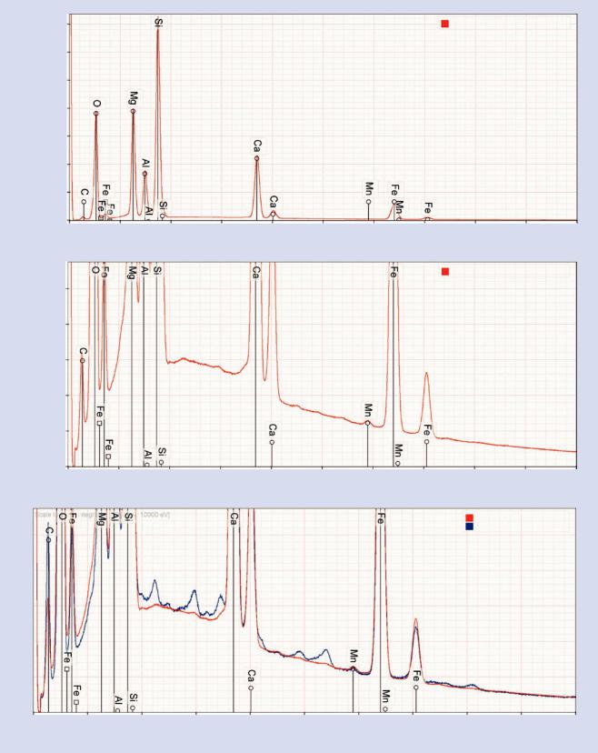
. Fig. 20.3 SDD-EDS spectra of NIST SRM (glass K412, E0 = 20 keV: a, b at 3 % dead-time (red); c 3 % (red) and 29 % dead-time (blue), showing in-growth of coincidence peaks
\316 Chapter 20 · Quantitative Analysis: The SEM/EDS Elemental Microanalysis k-ratio Procedure for Bulk Specimens, Step-by-Step
20.3\ Examples ofthek-ratio/Matrix Correction Protocol with DTSA II
(Newbury and Ritchie 2015b)
20.3.1\ Analysis of Major Constituents
(C > 0.1 Mass Fraction) with
Well-Resolved Peaks
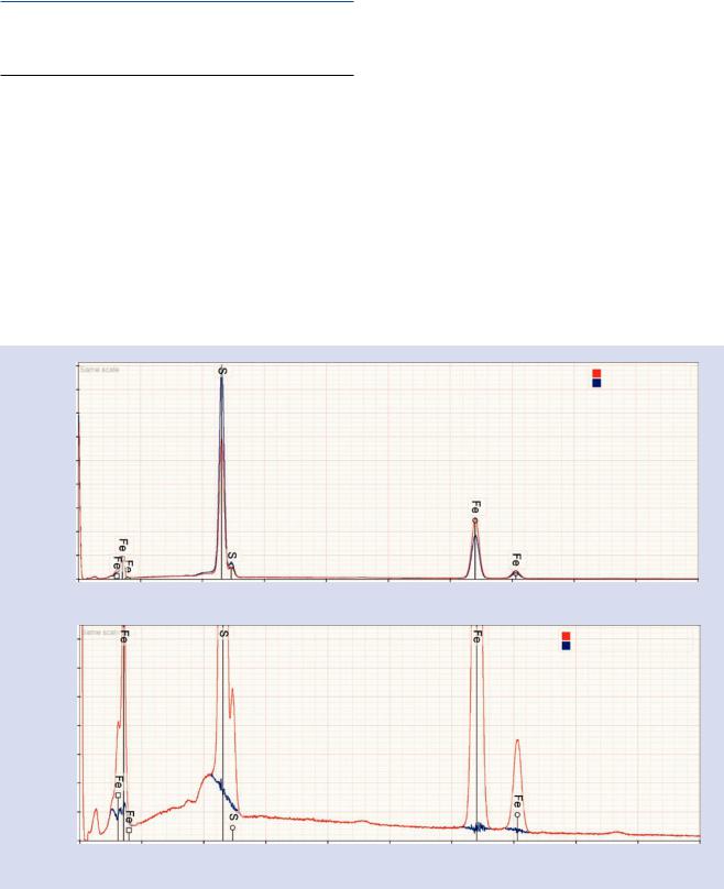
The EDS spectra of the minerals pyrite (FeS2) and troilite (FeS) measured at E0 =20 keV with a dead-time of~10% are shown in . Fig. 20.4 and feature well separated peaks for the Fe K- and L- families and the S K-family. These spectra were analyzed with Fe and CuS serving both as peak-fitting references and as standards. CuS is chosen for the S reference and standard rather than elemental S since CuS is stable under electron bombardment while elemental S is not stable. The spectrum for FeS and the residual spectrum after peak-fitting are also shown in . Fig. 20.4. The results for seven replicate analyses are listed in . Table 20.1 (FeS) and . Table 20.2 (FeS2) along with the ZAF correction factors and the components of
the error budget. In this analysis and the analyses reported below, the relative deviation from the expected value (RDEV) (also referred to as “relative error”) is calculated with the “expected” value taken as the stoichiometric formula value or the value obtained from an “absolute” analytical method, just as in gravimetric analysis:
|
( |
Analyzed value− expected value |
) |
|
|
|
RDEV = |
expected value |
|
× 100% |
\ (20.3) |
||
|
|
|
|
|
|
Optimizing Analysis Strategy
The DTSA II analysis report includes for each analyzed element the ZAF factors and the estimated uncertainties in these factors as well as uncertainties due to the counting statistics associated with the measurements of the unknown and of the standard (Ritchie and Newbury 2012). Careful examination of these factors can be used to refine the analytical strategy to optimize the measurement. Reducing the uncertainty due to the counting statistics requires increasing the dose. The absorption factor A is strongly influenced by the
a
Counts
b
|
Counts |
|
20 |
||
|
||
|
|
180 000 |
|
|
|
|
|
|
|
|
FeS_20kV10n9%DT_50s |
|
|
|
|
|
|
|
|
|
|
||
160 000 |
|
|
|
|
|
|
|
|
FeS_20kV10n9%DT_50s |
|
|
|
|
|
|
|
|
|
|
|
|
140 000 |
|
|
|
|
E0 = 20 KeV |
|
|
|
|
|
|
|
|
|
FeS |
|
|
|
|
|
|
|
|
|
|
|
|
|
|
|
|
|
120 000 |
|
|
|
|
FeS2 |
|
|
|
|
|
100 000 |
|
|
|
|
|
|
|
|
|
|
80 000 |
|
|
|
|
|
|
|
|
|
|
60 000 |
|
|
|
|
|
|
|
|
|
|
40 000 |
|
|
|
|
|
|
|
|
|
|
20 000 |
|
|
|
|
|
|
|
|
|
|
00.0 |
1.0 |
2.0 |
3.0 |
4.0 |
5.0 |
6.0 |
7.0 |
8.0 |
9.0 |
10.0 |
|
|
|
|
|
Photon energy (keV) |
|
|
|
|
|
14 000 |
|
|
|
|
|
|
|
FeS_20kV10n9%DT_50s |
|
|
|
|
|
|
|
|
|
|
Residual_FeS_20kV10n9%DT_50s |
||
12 000 |
|
|
|
|
|
|
|
|
|
|
10 000 |
|
|
|
E0 = 20 KeV |
|
|
|
|
|
|
|
|
|
FeS |
|
|
|
|
|
||
8 000 |
|
|
|
Fitting residual |
|
|
|
|
|
|
|
|
|
|
|
|
|
|
|
|
|
6 000 |
|
|
|
|
|
|
|
|
|
|
4 000 |
|
|
|
|
|
|
|
|
|
|
2 000 |
|
|
|
|
|
|
|
|
|
|
00.0 |
1.0 |
2.0 |
3.0 |
4.0 |
5.0 |
6.0 |
7.0 |
8.0 |
9.0 |
10.0 |
|
|
|
|
|
Photon energy (keV) |
|
|
|
|
|
. Fig. 20.4 a SDD-EDS spectra of Pyrite (FeS2) (blue) and meteoritic Troilite (FeS (red) at E0 = 20 keV. b NIST DTSA-II analysis of FeS using Fe and CuS as peak-fitting references and as standards. The original spectrum (red) and the residual spectrum after peak-fitting (blue) are shown

317 |
20 |
20.3 · Examples of the k-ratio/Matrix Correction Protocol with DTSA II
. Table 20.1 Analysis of FeS (meteoritic troilite) at E0 = 20 keV with CuS and Fe as fitting references and standards Integrated
spectrum count, 0.1–20 keV = 7,048,000; uncertainties expressed in mass fraction. Analysis performed with Fe K-L2,3 and S K-L2,3
|
S |
Fe |
Cav (atom frac) |
0.5052 |
0.4948 |
Z-correction |
0.977 |
0.95 |
A-correction |
1.118 |
0.983 |
F-correction |
1.003 |
1 |
σ (7 replicates) |
0.00075 |
0.00075 |
σRel (%) |
0.15 % |
0.15 % |
RDEV (%) |
1.00 % |
−1.00 % |
C (mass frac, single analysis) |
0.3699 |
0.6305 |
Counting error, std |
0.00020 |
0.0003 |
Counting error, unk |
0.00020 |
0.0007 |
A-factor error |
0.0017 |
0.0002 |
Z-factor error |
2.20×10⁵ |
4.10×10⁻⁶ |
Combined errors |
0.0017 |
0.0008 |
. Table 20.3 Analysis of FeS at E0 = 10 keV with CuS and Fe as fitting references and standards Integrated spectrum count,
0.1–10 keV = 5,630,000; uncertainties expressed in mass fraction. Analysis performed with Fe K-L2,3 and S K-L2,3
|
S |
Fe |
Cav (atom frac) |
0.503 |
0.497 |
Z-correction |
0.973 |
0.937 |
A-correction |
1.041 |
0.997 |
F-correction |
1.001 |
1 |
σ (7 replicates) |
0.00056 |
0.00056 |
σRel (%) |
0.11 % |
0.11 % |
RDEV (%) |
0.59 % |
−0.59 % |
C (mass frac, single analysis) |
0.3627 |
0.6257 |
Counting error, std |
0.0002 |
0.0008 |
Counting error, unk |
0.0003 |
0.0018 |
A-factor error |
0.0006 |
4.10E-05 |
Z-factor error |
2.20×10⁻⁵ |
1.30×10⁻⁶ |
Combined errors |
0.0007 |
0.0019 |
. Table 20.2 Analysis of FeS2 (pyrite) at E0 = 20 keV with CuS and Fe as fitting references and standards Integrated spectrum
count, 0.1.–20 keV = 7,765,000; uncertainties expressed in mass fraction. Analysis performed with Fe K-L2,3 and S K-L2,3
|
S |
Fe |
|
|
|
Cav (atom frac) |
0.6726 |
0.3274 |
Z-correction |
0.957 |
0.928 |
A-correction |
1.181 |
0.975 |
F-correction |
1.003 |
1 |
σ (7 replicates) |
0.000314 |
0.000314 |
σRel (%) |
0.05 % |
0.10 % |
RDEV (%) |
0.88 % |
−1.80 % |
C (mass frac, single analysis) |
0.5485 |
0.4657 |
Counting error, std |
0.0003 |
0.0002 |
Counting error, unk |
0.0003 |
0.0006 |
A-factor error |
0.0023 |
0.0002 |
Z-factor error |
3.30×10⁻⁵ |
2.90×10⁻⁶ |
Combined errors |
0.0023 |
0.0007 |
. Table 20.4 Analysis of FeS2 at E0 = 10 keV with CuS and Fe as fitting references and standards Integrated spectrum count,
0.1–10 keV = 6,253,000); uncertainties expressed in mass fraction. Analysis performed with Fe K-L2,3 and S K-L2,3
|
S |
Fe |
Cav (atom frac) |
0.671 |
0.329 |
Z-correction |
0.95 |
0.91 |
A-correction |
1.061 |
0.995 |
F-correction |
1.001 |
1 |
σ (7 replicates) |
0.0007 |
0.0007 |
σRel (%) |
0.11 % |
0.21 % |
RDEV (%) |
0.65 % |
−1.30 % |
C (mass frac, single analysis) |
0.537 |
0.4618 |
Counting error, std |
0.0003 |
0.0006 |
Counting error, unk |
0.0003 |
0.0016 |
A-factor error |
0.0008 |
4.30E-05 |
Z-factor error |
3.20×10⁻⁵ |
9.60×10⁻⁷ |
Combined errors |
0.0009 |
0.0017 |
choice of beam energy. If the beam energy can be decreased, considering also the constraints imposed by having sufficient overvoltage for all elements to be analyzed, the absorption correction factor and its uncertainty can also be reduced. For the Fe-S examples, lowering the beam energy from 20 to
10 keV gives the results shown in . Tables 20.3 and 20.4. The absorption factor A from is reduced from 1.118 to 1.04 for S in FeS and from 1.18 to 1.06 for S in FeS2, and the relative errors are also reduced slightly, from 1 to 0.59 % for S in FeS and from 0.88 to 0.65 % for S in FeS2.
\318 Chapter 20 · Quantitative Analysis: The SEM/EDS Elemental Microanalysis k-ratio Procedure for Bulk Specimens, Step-by-Step
20.3.2\ Analysis of Major Constituents
(C > 0.1 Mass Fraction) with Severely
Overlapping Peaks
PbS
The throughput and the peak stability (calibration and resolution) of SDD-EDS spectrometry enable collection of high count, high quality spectra (>5 million counts) within modest measurement time, 100 s or less. High count spectra enable measurements of minor and trace constituents with high precision. High counts and stable peak structures are critical for successful peak intensity measurements by peak- fitting methods, which is especially important for situations where two or more peaks are so close in photon energy that the EDS resolution function convolves the peaks into mutual interference. Despite extreme peak interference, quantitative X-ray microanalysis can be achieved with RDEV values of
5 % relative or less (Newbury and Ritchie 2015a).
PbS (galena) represents a challenging analysis situation for EDS because of the severe interference between the S K-L2 (2.307 keV) and Pb M5-N6,7 (2.343 keV), which are
separated by 36 eV, as shown in . Fig. 20.5. Analysis of PbS with DTSA II using CuS and PbSe as peak-fitting references and as standards yields the results in . Table 20.5. Despite the severe peak interference, the relative error based on the formula stoichiometry is only ±1.2 % for S and Pb.
Note that an alternative analytical approach would be to select the beam energy such that E0 ≥20 keV so that the Pb L-family is excited (LIII = 13.04 keV). With this choice of excitation, the Pb L3-M4,5 peak at 10.55 keV, which does not suffer interference, could be chosen to measure Pb. Of course, the S K still must be deconvoluted from the interference from the Pb M-family since there is no alternate peak to measure for S.
MoS2
MoS2 represents an even greater analytical challenge because the peaks that must be used for analysis, S K-L2 (2.307 keV)
and Mo L3-M4,5 (2.293 keV), are separated by only 14 eV, as shown in . Fig. 20.6. Analysis of MoS2 with DTSA II using
CuS and Mo as peak-fitting references and as standards yields the results in . Table 20.6. Despite the severe peak interference, the relative error based on the formula stoichiometry is only −0.34 % for S and 0.7 % for Mo.
|
|
a 120 000 |
|
|
|
|
|
|
|
|
|
PbS_10kV20nA |
|
|
|
|
|
|
|
|
|
|
|
|
|
|
Residual_PbS_10kV20nA |
|
|
|
100 000 |
|
|
|
|
|
|
E0 = 10 KeV |
|
|
|
|
|
|
|
|
|
|
|
|
|
|
|
|
|
|
|
|
|
|
|
|
|
|
|
PbS |
|
|
|
|
|
Counts |
80 000 |
|
|
|
|
|
|
Fitting residual |
|
|
|
|
|
60 000 |
|
|
|
|
|
|
|
|
|
|
|
|
|
|
|
|
|
|
|
|
|
|
|
|
|
|
|
|
40 000 |
|
|
|
|
|
|
|
|
|
|
|
|
|
20 000 |
|
|
|
|
|
|
|
|
|
|
|
|
|
0 |
1.5 |
1.7 |
1.9 |
2.1 |
2.3 |
2.5 |
2.7 |
2.9 |
3.1 |
3.3 |
|
|
|
|
|
|
|
|
Photon energy (keV) |
|
|
|
|
|
|
|
b |
|
|
|
|
|
|
|
|
|
|
PbS_10kV20nA |
|
|
|
14 000 |
|
|
|
|
|
|
|
|
|
|
|
|
|
|
|
|
|
|
|
|
|
|
Residual_PbS_10kV20nA |
|
|
|
|
12 000 |
|
|
|
|
|
|
|
|
|
|
|
|
|
10 000 |
|
|
|
|
|
|
|
|
|
|
|
|
Counts |
8 000 |
|
|
|
|
|
|
|
|
|
|
20 |
|
|
|
|
|
|
|
|
|
|
|||
|
|
|
|
|
|
|
|
|
|
|
|
|
|
|
|
|
6 000 |
|
|
|
|
|
|
|
|
|
|
|
|
|
|
|
|
|
|
|
|
|
|
|
|
|
|
|
4 000 |
|
|
|
|
|
|
|
|
|
|
|
|
|
2 000 |
|
|
|
|
|
|
|
|
|
|
|
|
|
0 |
1.5 |
1.7 |
1.9 |
2.1 |
2.3 |
2.5 |
2.7 |
2.9 |
3.1 |
3.3 |
|
|
|
|
|
|
|
|
Photon energy (keV) |
|
|
|
|
|
|
|
|
|
|
|
|
|
|
|
|
|
|
|
. Fig. 20.5 a SDD-EDS spectrum of PbS (red) and residual (blue) after DTSA II analysis using CuS and PbSe as fitting references and standards. b Expanded view