- •Preface
- •Imaging Microscopic Features
- •Measuring the Crystal Structure
- •References
- •Contents
- •1.4 Simulating the Effects of Elastic Scattering: Monte Carlo Calculations
- •What Are the Main Features of the Beam Electron Interaction Volume?
- •How Does the Interaction Volume Change with Composition?
- •How Does the Interaction Volume Change with Incident Beam Energy?
- •How Does the Interaction Volume Change with Specimen Tilt?
- •1.5 A Range Equation To Estimate the Size of the Interaction Volume
- •References
- •2: Backscattered Electrons
- •2.1 Origin
- •2.2.1 BSE Response to Specimen Composition (η vs. Atomic Number, Z)
- •SEM Image Contrast with BSE: “Atomic Number Contrast”
- •SEM Image Contrast: “BSE Topographic Contrast—Number Effects”
- •2.2.3 Angular Distribution of Backscattering
- •Beam Incident at an Acute Angle to the Specimen Surface (Specimen Tilt > 0°)
- •SEM Image Contrast: “BSE Topographic Contrast—Trajectory Effects”
- •2.2.4 Spatial Distribution of Backscattering
- •Depth Distribution of Backscattering
- •Radial Distribution of Backscattered Electrons
- •2.3 Summary
- •References
- •3: Secondary Electrons
- •3.1 Origin
- •3.2 Energy Distribution
- •3.3 Escape Depth of Secondary Electrons
- •3.8 Spatial Characteristics of Secondary Electrons
- •References
- •4: X-Rays
- •4.1 Overview
- •4.2 Characteristic X-Rays
- •4.2.1 Origin
- •4.2.2 Fluorescence Yield
- •4.2.3 X-Ray Families
- •4.2.4 X-Ray Nomenclature
- •4.2.6 Characteristic X-Ray Intensity
- •Isolated Atoms
- •X-Ray Production in Thin Foils
- •X-Ray Intensity Emitted from Thick, Solid Specimens
- •4.3 X-Ray Continuum (bremsstrahlung)
- •4.3.1 X-Ray Continuum Intensity
- •4.3.3 Range of X-ray Production
- •4.4 X-Ray Absorption
- •4.5 X-Ray Fluorescence
- •References
- •5.1 Electron Beam Parameters
- •5.2 Electron Optical Parameters
- •5.2.1 Beam Energy
- •Landing Energy
- •5.2.2 Beam Diameter
- •5.2.3 Beam Current
- •5.2.4 Beam Current Density
- •5.2.5 Beam Convergence Angle, α
- •5.2.6 Beam Solid Angle
- •5.2.7 Electron Optical Brightness, β
- •Brightness Equation
- •5.2.8 Focus
- •Astigmatism
- •5.3 SEM Imaging Modes
- •5.3.1 High Depth-of-Field Mode
- •5.3.2 High-Current Mode
- •5.3.3 Resolution Mode
- •5.3.4 Low-Voltage Mode
- •5.4 Electron Detectors
- •5.4.1 Important Properties of BSE and SE for Detector Design and Operation
- •Abundance
- •Angular Distribution
- •Kinetic Energy Response
- •5.4.2 Detector Characteristics
- •Angular Measures for Electron Detectors
- •Elevation (Take-Off) Angle, ψ, and Azimuthal Angle, ζ
- •Solid Angle, Ω
- •Energy Response
- •Bandwidth
- •5.4.3 Common Types of Electron Detectors
- •Backscattered Electrons
- •Passive Detectors
- •Scintillation Detectors
- •Semiconductor BSE Detectors
- •5.4.4 Secondary Electron Detectors
- •Everhart–Thornley Detector
- •Through-the-Lens (TTL) Electron Detectors
- •TTL SE Detector
- •TTL BSE Detector
- •Measuring the DQE: BSE Semiconductor Detector
- •References
- •6: Image Formation
- •6.1 Image Construction by Scanning Action
- •6.2 Magnification
- •6.3 Making Dimensional Measurements With the SEM: How Big Is That Feature?
- •Using a Calibrated Structure in ImageJ-Fiji
- •6.4 Image Defects
- •6.4.1 Projection Distortion (Foreshortening)
- •6.4.2 Image Defocusing (Blurring)
- •6.5 Making Measurements on Surfaces With Arbitrary Topography: Stereomicroscopy
- •6.5.1 Qualitative Stereomicroscopy
- •Fixed beam, Specimen Position Altered
- •Fixed Specimen, Beam Incidence Angle Changed
- •6.5.2 Quantitative Stereomicroscopy
- •Measuring a Simple Vertical Displacement
- •References
- •7: SEM Image Interpretation
- •7.1 Information in SEM Images
- •7.2.2 Calculating Atomic Number Contrast
- •Establishing a Robust Light-Optical Analogy
- •Getting It Wrong: Breaking the Light-Optical Analogy of the Everhart–Thornley (Positive Bias) Detector
- •Deconstructing the SEM/E–T Image of Topography
- •SUM Mode (A + B)
- •DIFFERENCE Mode (A−B)
- •References
- •References
- •9: Image Defects
- •9.1 Charging
- •9.1.1 What Is Specimen Charging?
- •9.1.3 Techniques to Control Charging Artifacts (High Vacuum Instruments)
- •Observing Uncoated Specimens
- •Coating an Insulating Specimen for Charge Dissipation
- •Choosing the Coating for Imaging Morphology
- •9.2 Radiation Damage
- •9.3 Contamination
- •References
- •10: High Resolution Imaging
- •10.2 Instrumentation Considerations
- •10.4.1 SE Range Effects Produce Bright Edges (Isolated Edges)
- •10.4.4 Too Much of a Good Thing: The Bright Edge Effect Hinders Locating the True Position of an Edge for Critical Dimension Metrology
- •10.5.1 Beam Energy Strategies
- •Low Beam Energy Strategy
- •High Beam Energy Strategy
- •Making More SE1: Apply a Thin High-δ Metal Coating
- •Making Fewer BSEs, SE2, and SE3 by Eliminating Bulk Scattering From the Substrate
- •10.6 Factors That Hinder Achieving High Resolution
- •10.6.2 Pathological Specimen Behavior
- •Contamination
- •Instabilities
- •References
- •11: Low Beam Energy SEM
- •11.3 Selecting the Beam Energy to Control the Spatial Sampling of Imaging Signals
- •11.3.1 Low Beam Energy for High Lateral Resolution SEM
- •11.3.2 Low Beam Energy for High Depth Resolution SEM
- •11.3.3 Extremely Low Beam Energy Imaging
- •References
- •12.1.1 Stable Electron Source Operation
- •12.1.2 Maintaining Beam Integrity
- •12.1.4 Minimizing Contamination
- •12.3.1 Control of Specimen Charging
- •12.5 VPSEM Image Resolution
- •References
- •13: ImageJ and Fiji
- •13.1 The ImageJ Universe
- •13.2 Fiji
- •13.3 Plugins
- •13.4 Where to Learn More
- •References
- •14: SEM Imaging Checklist
- •14.1.1 Conducting or Semiconducting Specimens
- •14.1.2 Insulating Specimens
- •14.2 Electron Signals Available
- •14.2.1 Beam Electron Range
- •14.2.2 Backscattered Electrons
- •14.2.3 Secondary Electrons
- •14.3 Selecting the Electron Detector
- •14.3.2 Backscattered Electron Detectors
- •14.3.3 “Through-the-Lens” Detectors
- •14.4 Selecting the Beam Energy for SEM Imaging
- •14.4.4 High Resolution SEM Imaging
- •Strategy 1
- •Strategy 2
- •14.5 Selecting the Beam Current
- •14.5.1 High Resolution Imaging
- •14.5.2 Low Contrast Features Require High Beam Current and/or Long Frame Time to Establish Visibility
- •14.6 Image Presentation
- •14.6.1 “Live” Display Adjustments
- •14.6.2 Post-Collection Processing
- •14.7 Image Interpretation
- •14.7.1 Observer’s Point of View
- •14.7.3 Contrast Encoding
- •14.8.1 VPSEM Advantages
- •14.8.2 VPSEM Disadvantages
- •15: SEM Case Studies
- •15.1 Case Study: How High Is That Feature Relative to Another?
- •15.2 Revealing Shallow Surface Relief
- •16.1.2 Minor Artifacts: The Si-Escape Peak
- •16.1.3 Minor Artifacts: Coincidence Peaks
- •16.1.4 Minor Artifacts: Si Absorption Edge and Si Internal Fluorescence Peak
- •16.2 “Best Practices” for Electron-Excited EDS Operation
- •16.2.1 Operation of the EDS System
- •Choosing the EDS Time Constant (Resolution and Throughput)
- •Choosing the Solid Angle of the EDS
- •Selecting a Beam Current for an Acceptable Level of System Dead-Time
- •16.3.1 Detector Geometry
- •16.3.2 Process Time
- •16.3.3 Optimal Working Distance
- •16.3.4 Detector Orientation
- •16.3.5 Count Rate Linearity
- •16.3.6 Energy Calibration Linearity
- •16.3.7 Other Items
- •16.3.8 Setting Up a Quality Control Program
- •Using the QC Tools Within DTSA-II
- •Creating a QC Project
- •Linearity of Output Count Rate with Live-Time Dose
- •Resolution and Peak Position Stability with Count Rate
- •Solid Angle for Low X-ray Flux
- •Maximizing Throughput at Moderate Resolution
- •References
- •17: DTSA-II EDS Software
- •17.1 Getting Started With NIST DTSA-II
- •17.1.1 Motivation
- •17.1.2 Platform
- •17.1.3 Overview
- •17.1.4 Design
- •Simulation
- •Quantification
- •Experiment Design
- •Modeled Detectors (. Fig. 17.1)
- •Window Type (. Fig. 17.2)
- •The Optimal Working Distance (. Figs. 17.3 and 17.4)
- •Elevation Angle
- •Sample-to-Detector Distance
- •Detector Area
- •Crystal Thickness
- •Number of Channels, Energy Scale, and Zero Offset
- •Resolution at Mn Kα (Approximate)
- •Azimuthal Angle
- •Gold Layer, Aluminum Layer, Nickel Layer
- •Dead Layer
- •Zero Strobe Discriminator (. Figs. 17.7 and 17.8)
- •Material Editor Dialog (. Figs. 17.9, 17.10, 17.11, 17.12, 17.13, and 17.14)
- •17.2.1 Introduction
- •17.2.2 Monte Carlo Simulation
- •17.2.4 Optional Tables
- •References
- •18: Qualitative Elemental Analysis by Energy Dispersive X-Ray Spectrometry
- •18.1 Quality Assurance Issues for Qualitative Analysis: EDS Calibration
- •18.2 Principles of Qualitative EDS Analysis
- •Exciting Characteristic X-Rays
- •Fluorescence Yield
- •X-ray Absorption
- •Si Escape Peak
- •Coincidence Peaks
- •18.3 Performing Manual Qualitative Analysis
- •Beam Energy
- •Choosing the EDS Resolution (Detector Time Constant)
- •Obtaining Adequate Counts
- •18.4.1 Employ the Available Software Tools
- •18.4.3 Lower Photon Energy Region
- •18.4.5 Checking Your Work
- •18.5 A Worked Example of Manual Peak Identification
- •References
- •19.1 What Is a k-ratio?
- •19.3 Sets of k-ratios
- •19.5 The Analytical Total
- •19.6 Normalization
- •19.7.1 Oxygen by Assumed Stoichiometry
- •19.7.3 Element by Difference
- •19.8 Ways of Reporting Composition
- •19.8.1 Mass Fraction
- •19.8.2 Atomic Fraction
- •19.8.3 Stoichiometry
- •19.8.4 Oxide Fractions
- •Example Calculations
- •19.9 The Accuracy of Quantitative Electron-Excited X-ray Microanalysis
- •19.9.1 Standards-Based k-ratio Protocol
- •19.9.2 “Standardless Analysis”
- •19.10 Appendix
- •19.10.1 The Need for Matrix Corrections To Achieve Quantitative Analysis
- •19.10.2 The Physical Origin of Matrix Effects
- •19.10.3 ZAF Factors in Microanalysis
- •X-ray Generation With Depth, φ(ρz)
- •X-ray Absorption Effect, A
- •X-ray Fluorescence, F
- •References
- •20.2 Instrumentation Requirements
- •20.2.1 Choosing the EDS Parameters
- •EDS Spectrum Channel Energy Width and Spectrum Energy Span
- •EDS Time Constant (Resolution and Throughput)
- •EDS Calibration
- •EDS Solid Angle
- •20.2.2 Choosing the Beam Energy, E0
- •20.2.3 Measuring the Beam Current
- •20.2.4 Choosing the Beam Current
- •Optimizing Analysis Strategy
- •20.3.4 Ba-Ti Interference in BaTiSi3O9
- •20.4 The Need for an Iterative Qualitative and Quantitative Analysis Strategy
- •20.4.2 Analysis of a Stainless Steel
- •20.5 Is the Specimen Homogeneous?
- •20.6 Beam-Sensitive Specimens
- •20.6.1 Alkali Element Migration
- •20.6.2 Materials Subject to Mass Loss During Electron Bombardment—the Marshall-Hall Method
- •Thin Section Analysis
- •Bulk Biological and Organic Specimens
- •References
- •21: Trace Analysis by SEM/EDS
- •21.1 Limits of Detection for SEM/EDS Microanalysis
- •21.2.1 Estimating CDL from a Trace or Minor Constituent from Measuring a Known Standard
- •21.2.2 Estimating CDL After Determination of a Minor or Trace Constituent with Severe Peak Interference from a Major Constituent
- •21.3 Measurements of Trace Constituents by Electron-Excited Energy Dispersive X-ray Spectrometry
- •The Inevitable Physics of Remote Excitation Within the Specimen: Secondary Fluorescence Beyond the Electron Interaction Volume
- •Simulation of Long-Range Secondary X-ray Fluorescence
- •NIST DTSA II Simulation: Vertical Interface Between Two Regions of Different Composition in a Flat Bulk Target
- •NIST DTSA II Simulation: Cubic Particle Embedded in a Bulk Matrix
- •21.5 Summary
- •References
- •22.1.2 Low Beam Energy Analysis Range
- •22.2 Advantage of Low Beam Energy X-Ray Microanalysis
- •22.2.1 Improved Spatial Resolution
- •22.3 Challenges and Limitations of Low Beam Energy X-Ray Microanalysis
- •22.3.1 Reduced Access to Elements
- •22.3.3 At Low Beam Energy, Almost Everything Is Found To Be Layered
- •Analysis of Surface Contamination
- •References
- •23: Analysis of Specimens with Special Geometry: Irregular Bulk Objects and Particles
- •23.2.1 No Chemical Etching
- •23.3 Consequences of Attempting Analysis of Bulk Materials With Rough Surfaces
- •23.4.1 The Raw Analytical Total
- •23.4.2 The Shape of the EDS Spectrum
- •23.5 Best Practices for Analysis of Rough Bulk Samples
- •23.6 Particle Analysis
- •Particle Sample Preparation: Bulk Substrate
- •The Importance of Beam Placement
- •Overscanning
- •“Particle Mass Effect”
- •“Particle Absorption Effect”
- •The Analytical Total Reveals the Impact of Particle Effects
- •Does Overscanning Help?
- •23.6.6 Peak-to-Background (P/B) Method
- •Specimen Geometry Severely Affects the k-ratio, but Not the P/B
- •Using the P/B Correspondence
- •23.7 Summary
- •References
- •24: Compositional Mapping
- •24.2 X-Ray Spectrum Imaging
- •24.2.1 Utilizing XSI Datacubes
- •24.2.2 Derived Spectra
- •SUM Spectrum
- •MAXIMUM PIXEL Spectrum
- •24.3 Quantitative Compositional Mapping
- •24.4 Strategy for XSI Elemental Mapping Data Collection
- •24.4.1 Choosing the EDS Dead-Time
- •24.4.2 Choosing the Pixel Density
- •24.4.3 Choosing the Pixel Dwell Time
- •“Flash Mapping”
- •High Count Mapping
- •References
- •25.1 Gas Scattering Effects in the VPSEM
- •25.1.1 Why Doesn’t the EDS Collimator Exclude the Remote Skirt X-Rays?
- •25.2 What Can Be Done To Minimize gas Scattering in VPSEM?
- •25.2.2 Favorable Sample Characteristics
- •Particle Analysis
- •25.2.3 Unfavorable Sample Characteristics
- •References
- •26.1 Instrumentation
- •26.1.2 EDS Detector
- •26.1.3 Probe Current Measurement Device
- •Direct Measurement: Using a Faraday Cup and Picoammeter
- •A Faraday Cup
- •Electrically Isolated Stage
- •Indirect Measurement: Using a Calibration Spectrum
- •26.1.4 Conductive Coating
- •26.2 Sample Preparation
- •26.2.1 Standard Materials
- •26.2.2 Peak Reference Materials
- •26.3 Initial Set-Up
- •26.3.1 Calibrating the EDS Detector
- •Selecting a Pulse Process Time Constant
- •Energy Calibration
- •Quality Control
- •Sample Orientation
- •Detector Position
- •Probe Current
- •26.4 Collecting Data
- •26.4.1 Exploratory Spectrum
- •26.4.2 Experiment Optimization
- •26.4.3 Selecting Standards
- •26.4.4 Reference Spectra
- •26.4.5 Collecting Standards
- •26.4.6 Collecting Peak-Fitting References
- •26.5 Data Analysis
- •26.5.2 Quantification
- •26.6 Quality Check
- •Reference
- •27.2 Case Study: Aluminum Wire Failures in Residential Wiring
- •References
- •28: Cathodoluminescence
- •28.1 Origin
- •28.2 Measuring Cathodoluminescence
- •28.3 Applications of CL
- •28.3.1 Geology
- •Carbonado Diamond
- •Ancient Impact Zircons
- •28.3.2 Materials Science
- •Semiconductors
- •Lead-Acid Battery Plate Reactions
- •28.3.3 Organic Compounds
- •References
- •29.1.1 Single Crystals
- •29.1.2 Polycrystalline Materials
- •29.1.3 Conditions for Detecting Electron Channeling Contrast
- •Specimen Preparation
- •Instrument Conditions
- •29.2.1 Origin of EBSD Patterns
- •29.2.2 Cameras for EBSD Pattern Detection
- •29.2.3 EBSD Spatial Resolution
- •29.2.5 Steps in Typical EBSD Measurements
- •Sample Preparation for EBSD
- •Align Sample in the SEM
- •Check for EBSD Patterns
- •Adjust SEM and Select EBSD Map Parameters
- •Run the Automated Map
- •29.2.6 Display of the Acquired Data
- •29.2.7 Other Map Components
- •29.2.10 Application Example
- •Application of EBSD To Understand Meteorite Formation
- •29.2.11 Summary
- •Specimen Considerations
- •EBSD Detector
- •Selection of Candidate Crystallographic Phases
- •Microscope Operating Conditions and Pattern Optimization
- •Selection of EBSD Acquisition Parameters
- •Collect the Orientation Map
- •References
- •30.1 Introduction
- •30.2 Ion–Solid Interactions
- •30.3 Focused Ion Beam Systems
- •30.5 Preparation of Samples for SEM
- •30.5.1 Cross-Section Preparation
- •30.5.2 FIB Sample Preparation for 3D Techniques and Imaging
- •30.6 Summary
- •References
- •31: Ion Beam Microscopy
- •31.1 What Is So Useful About Ions?
- •31.2 Generating Ion Beams
- •31.3 Signal Generation in the HIM
- •31.5 Patterning with Ion Beams
- •31.7 Chemical Microanalysis with Ion Beams
- •References
- •Appendix
- •A Database of Electron–Solid Interactions
- •Introduction
- •Backscattered Electrons
- •Secondary Yields
- •Stopping Powers
- •X-ray Ionization Cross Sections
- •Conclusions
- •References
- •Index
- •Reference List
- •Index
29 |
|
3 |
|
|
|
Secondary Electrons
3.1\ Origin – 30
3.2\ Energy Distribution – 30
3.3\ Escape Depth of Secondary Electrons – 30
3.4\ Secondary Electron Yield Versus Atomic Number – 30 3.5\ Secondary Electron Yield Versus Specimen Tilt – 34 3.6\ Angular Distribution of Secondary Electrons – 34 3.7\ Secondary Electron Yield Versus Beam Energy – 35 3.8\ Spatial Characteristics of Secondary Electrons – 35
\References – 37
Electronic supplementary material The online version of this chapter (https://doi.org/10.1007/978-1-4939-6676-9_3) contains supplementary material, which is available to authorized users.
© Springer Science+Business Media LLC 2018
J. Goldstein et al., Scanning Electron Microscopy and X-Ray Microanalysis, https://doi.org/10.1007/978-1-4939-6676-9_3
\30 Chapter 3 · Secondary Electrons
3.1\ Origin
Secondary electrons (SE) are created when inelastic scattering of the beam electrons ejects weakly bound valence electrons (in the case of ionically or covalently bonded materials)
3 or conduction band electrons (in the case of metals), which have binding energies of ~ 1–15 eV to the parent atom(s). Secondary electrons are quantified by the parameter δ, which is the ratio of secondary electrons emitted from the specimen, NSE, to the number of incident beam (primary) electrons, NB:
d=NSE / NB \ |
(3.1) |
3.2\ Energy Distribution
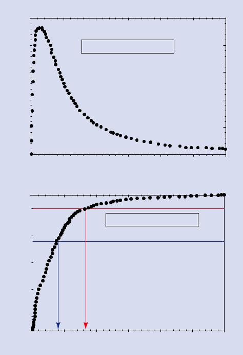
The most important characteristic of SE is their extremely low kinetic energy. Because of the large mismatch in relative velocities between the primary beam electron (incident energy 1–30 keV) and the weakly bound atomic electrons (1–15 eV ionization energy), the transfer of kinetic energy from the primary electron to the SE is relatively small, and as a result, the SE are ejected with low kinetic energy. After ejection, the SE must propagate through the specimen while undergoing inelastic scattering, which further decreases their kinetic energy. SE are generated along the complete trajectory of the beam electron within the specimen, but only a very small fraction of SE reach the surface with sufficient kinetic energy to exceed the surface energy barrier and escape. The energy spectrum of the secondary electrons that escape is peaked at only a few eV, as shown in . Fig. 3.1a for a measurement of a copper target and an incident beam energy of E0 = 1 keV. Above this peak, the intensity falls rapidly at higher kinetic energy (Koshikawa and Shimizu 1973).
. Figure 3.1b shows the cumulative intensity as a function of energy: 67 % of the secondary electrons from copper are emitted with less than 4 eV, and 90 % have less than 8.4 eV. Secondary electron production is considered to cease for kinetic energies above 50 eV, an arbitrary but reasonable value considering how sharply the energy distribution of
. Fig. 3.1a is skewed toward low energy. Inspection of the literature of secondary electrons confirms that the distribution for copper is generally representative of a large range of metals and other materials (e.g., Kanaya and Ono 1984).
3.3\ Escape Depth of Secondary Electrons
The kinetic energy of SE is so low that it has a strong influence on the depth from which SE can escape from the specimen. While some inelastic scattering processes are absent because of the low kinetic energy of SE, nevertheless SE suffer rapid energy loss with distance traveled, limiting the range of an SE
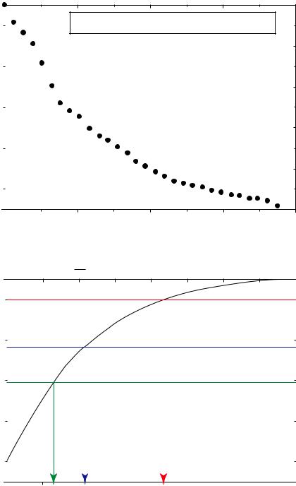
to a few nanometers rather than the hundreds to thousands of nanometers for the energetic beam electrons and BSE. Thus, although SE are generated along the entire trajectory of a beam electron scattering in the target, only those SE generated close to a surface have a significant chance to escape. The probability of escape depends on the initial kinetic energy, the depth of generation, and the nature of the host material. Since there is a spectrum of initial kinetic energies, each energy represents a different escape probability and depth sensitivity. This complex behavior is difficult to measure directly, and instead researchers have made use of the Monte Carlo simulation to characterize the escape depth. . Figure 3.2a shows the relative intensity of secondary electrons (over the energy range 0–50 eV) that escape from a copper target as a function of the depth of generation in the solid (Koshikawa and Shimizu 1974). . Figure 3.2b shows this same data in the form of the cumulative secondary electron intensity as a function of initial generation depth. For copper, virtually no secondary electron escapes if it is created below approximately 8 nm from the surface, and 67% of the secondary emission originates from a depth of less than 2.2 nm and 90% from less than 4.4 nm. Kanaya and Ono (1984) modeled the mean secondary electron escape depth, desc, in terms of various material parameters:
desc (nm) = 0.267 A I / (rZ0.66 ) |
\ |
(3.2) |
|
|
where A is the atomic weight (g/mol), ρ is the density (g/ cm3), Z is the atomic number, and I is the first ionization potential (eV). When this model is applied to the solid elements of the Periodic Table, the complex behavior seen in
. Fig. 3.3 results. The mean escape depth varies from a low value of ~ 0.25 nm for Ce to a high value of 9 nm for Li. For
copper, desc is calculated to be 1.8 nm, which can be compared to the 50 % escape value of 1.3 nm from the Monte
Carlo simulation study in . Fig. 3.2b. Systematic behavior of the atomic properties in Eq. 3.1 leads to systematic trends in the mean escape depth, with the low density alkali metals showing the largest values for the escape depth, while minima occur for the highest density elements in each period.
3.4\ Secondary Electron Yield Versus
Atomic Number
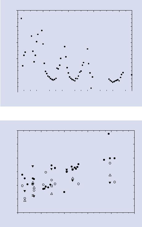
. Figure 3.4 shows a plot of the secondary electron coefficient as a function of atomic number for an incident beam energy of E0 = 5 keV with data taken from A Database of Electron-Solid Interactions of Joy (2012). The measurements of δ are chaotic and inconsistent. For example, the values of
δ for gold reported by various workers range from approximately 0.4 to 1.2. Oddly, all of these measured values may be “correct” in the sense that a valid, reproducible measurement was made on the particular specimen used. This behavior is really an indication of how difficult it is to make a
3.4 · Secondary Electron Yield Versus Atomic Number
. Fig. 3.1 a Secondary electron |
|
|
|
|
|
energy spectrum for copper with an |
|
|
|
|
|
incident beam energy of E0 = 1 keV |
a |
500 |
|
|
|
|
|
||||
(Koshikawa and Shimizu 1973). b |
|
|
|
|
|
(Data from . Fig. 3.1a replotted as |
|
|
|
|
|
the cumulative energy distribution) |
|
|
|
|
|
|
|
400 |
|
|
|
|
units) |
300 |
|
|
|
|
(arbitrary |
200 |
|
|
|
|
N(E) |
|
|
|
|
|
|
|
|
|
|
|
|
100 |
|
|
|
|
|
0 |
|
|
|
|
|
|
|
||
|
|
0 |
|||
|
b |
1.0 |
|
|
|
|
|
|
|||
|
emission |
0.8 |
|
|
|
|
electron |
0.6 |
|
|
|
|
secondary |
|
|
|
|
|
0.4 |
|
|
|
|
|
Cumulative |
|
|
|
|
|
0.2 |
|
|
|
|
|
|
|
|
|
|
|
|
0.0 |
|
|
|
|
|
|
|
||
|
|
0 |
31 |
|
3 |
|
|
|
Secondary electron energy spectrum for Cu (E0 = 1 keV)
Koshikawa & Shimizu (1973) data
5 |
10 |
15 |
20 |
25 |
30 |
|
|
Energy (eV) |
|
|
|
Cumulative secondary electron energy distribution (Cu, E0 = 1 keV)
Koshikawa & Shimizu (1973) data
4 eV |
8.4 eV |
|
5 |
10 |
15 |
20 |
25 |
30 |
|
Secondary electron energy (eV) |
|
|
representative measurement of a property that results from very low energy electrons generated within and escaping from a very shallow layer below the surface. Thus, a surface modified by accumulations of oxide and contamination (e.g., adsorbed water, chemisorbed water, hydrocarbons, etc.) is likely to produce a value of δ that is different from
the “ideal” pure element or pure compound value. If the specimen is pre-cleaned by ion bombardment in an ultrahigh vacuum electron beam instrument (chamber pressure maintained below 10−8 Pa) which preserves the clean surface, and if the surface composition is confirmed to be that of the pure element or compound by a surface-specific
|
32\ |
Chapter 3 · Secondary Electrons |
|
|
|
|
|
|
|
. Fig. 3.2 a Escape of secondary |
a |
|
|
|
|
|
|
|
electrons from copper as a function of |
|
1.0 |
|
|
|
|
|
|
|
|
|
|||||
|
generation depth from Monte Carlo |
|
|
|
|
|
|
|
|
simulation (Koshikawa and Shimizu |
units) |
|
|
|
|
|
|
|
1974). b (Data from . Fig. 3.2a |
|
|
|
|
|
||
|
|
|
|
|
|
|
||
|
replotted to show the cumulative |
(arbitrary |
0.8 |
|
|
|
|
|
3 |
escape of secondary electrons as a |
|
|
|
|
|||
|
|
|
|
|
||||
|
|
|
|
|
|
|||
function of depth of generation) |
|
|
|
|
|
|
||
|
|
|
electrons |
0.6 |
|
|
|
|
|
|
|
|
|
|
|
||
|
|
|
secondaryof |
|
|
|
|
|
|
|
|
0.4 |
|
|
|
|
|
|
|
|
Intensity |
|
|
|
|
|
|
|
|
0.2 |
|
|
|
|
|
|
|
|
|
|
|
|
|
|
|
|
|
|
0.0 |
|
|
|
|
|
|
|
|
0 |
||||
|
|
|
b |
|
|
|
|
|
|
|
|
|
1.0 |
|
|
|
|
|
|
|
|
|
|
|
|
|
|
|
|
intensitySE |
0.8 |
|
|
|
|
|
|
|
|
|
|
|
||
|
|
|
0.6 |
|
|
|
|
|
|
|
|
Cumulative |
|
|
|
|
|
|
|
|
0.4 |
|
|
|
|
|
|
|
|
|
|
|
|
|
|
|
|
|
|
0.2 |
|
|
|
|
|
|
|
|
|
|
|
|
|
|
|
|
|
0.0 |
|
|
|
|
|
|
|
|
0 |
Secondary electron escape depth for Cu
Koshikawa & Shimizu (1974) Monte Carlo calculation
2 |
4 |
6 |
8 |
|
Depth (nm) |
|
|
Cumulative secondary electron emission for copper
Koshikawa-Shimizu (1974) Monte Carlo
1.3 nm |
|
2.2 nm |
|
|
|
4.4 nm |
|
|
|
|||
|
|
|
|
|
|
|
||||||
|
|
|
|
|
|
|
||||||
|
|
|
|
|
|
|
||||||
|
|
|
|
|
|
|
||||||
|
|
|
|
|
|
|
||||||
|
|
|
|
|
|
|
||||||
|
|
|
|
|
|
|
|
|
||||
|
|
|
|
|
|
|
|
|
|
|
|
|
|
|
|
|
|
|
|
|
|
|
|
|
|
|
|
|
|
|
|
|
|
|
|
|
|
|
2 |
|
|
4 |
6 |
8 |
|||||||
|
|
|
|
Depth |
(nm) |
|
|
|
measurement method such as Auger electron spectroscopy or X-ray photoelectron spectroscopy, then the measured secondary electron coefficient is likely to be representative of the pure substance. However, the surfaces of most specimens examined in the conventional-vacuum SEM (chamber
pressure ~ 10−4 Pa) or a variable pressure SEM (chamber pressure from 10−4 Pa to values as high as 2500 Pa) are not likely to be that of pure substances, but are almost inevitably covered with a complex mixture of oxides, hydrocarbons, and chemisorbed water molecules that quickly redeposit
3.4 · Secondary Electron Yield Versus Atomic Number
. Fig. 3.3 Mean secondary electron |
|
|
escape depth for various materials as |
|
|
modeled by Kanaya and Ono (1984) |
|
10 |
|
|
8 |
|
(nm) |
6 |
|
depth |
|
|
|
|
|
Escape |
4 |
|
|
2
0
33 |
|
3 |
|
|
|
Secondary electron escape depth
Li
Kanaya-Ono (1984) calculations
K
Na
Rb
Cs
C
|
|
AI |
|
|
|
|
|
|
|
|
|
|
|
|
||
|
|
Be |
|
|
|
|
|
|
|
|
|
Bi |
||||
|
|
|
|
|
|
|
|
|
|
|
Hf |
|
|
|
|
Th |
|
|
|
|
|
|
|
|
|
|
|
|
|
|
|
||
|
|
|
|
|
|
|
|
|
|
|
|
|
|
|
|
|
|
|
|
|
Ni |
|
|
Rh |
Ce |
|
Re |
||||||
|
|
|
|
|
|
|
|
|
||||||||
|
|
|
|
|
|
|
|
|
|
|
|
|
|
|||
|
|
|
|
|
|
|
|
|
|
|
|
|
|
|
|
|
0 |
20 |
40 |
60 |
|
80 |
|
|
|||||||||
|
|
|
|
|
Atomic number |
|
|
|
|
|
|
|
|
|
. Fig. 3.4 Secondary electron coefficient as a function of atomic number for E0 = 5 keV (Data from the secondary electron database of Joy (2012))
Secondary electron coefficient
1.2
1.0
0.8
0.6
0.4
0.2
0.0
0
Secondary electron yield vs. atomic number (E0 = 5 keV)
|
|
|
|
|
|
|
|
|
|
|
|
|
|
|
|
|
|
|
|
|
|
|
|
|
|
|
|
|
|
|
|
|
|
|
|
|
|
|
|
20 |
40 |
60 |
80 |
100 |
|||
|
|
|
Atomic number |
|
|
|
at such elevated pressures even when ion beam cleaning is utilized to expose the “true” surface. The effective secondary electron coefficient of a “real” material under typical SEM or VP-SEM vacuum conditions is unlikely to produce a consistent, predictable response as a function of the composition of the nominal substance under examination.
Thus, while compositionally dependent secondary electron signals may be occasionally observed, they are generally not predictable and reproducible, which is the critical basis for establishing a useful contrast mechanism such as that found for backscattered electrons as a function of atomic number.
\34 Chapter 3 · Secondary Electrons
3.5\ Secondary Electron Yield Versus
Specimen Tilt
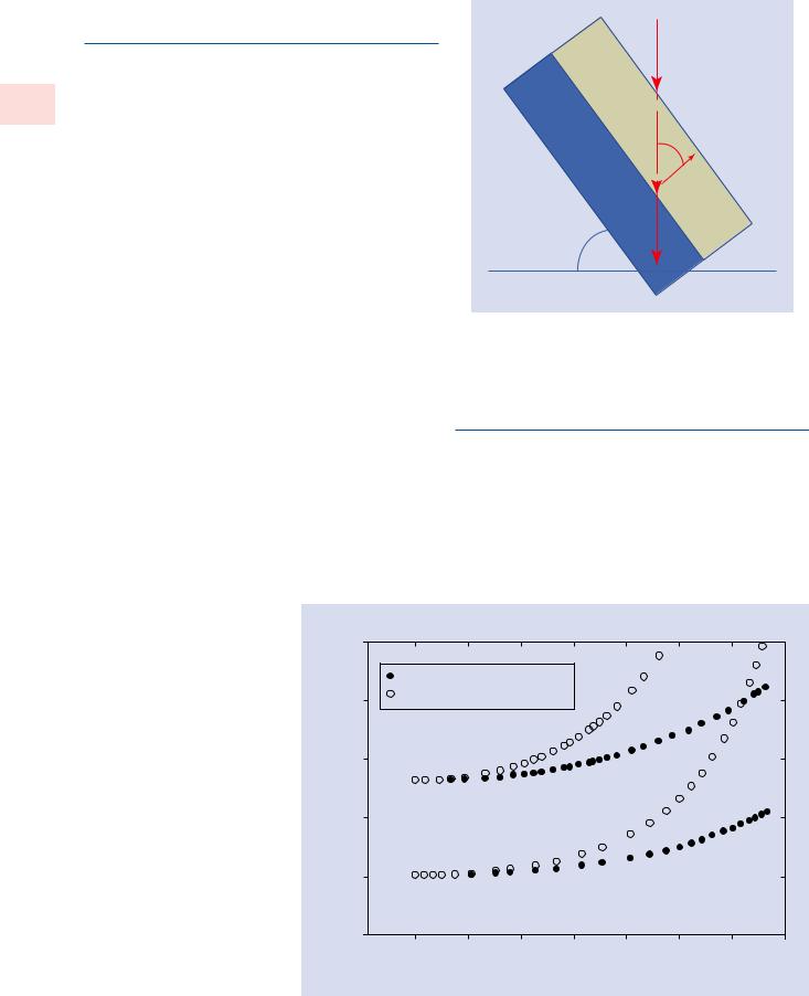
When the secondary electron coefficient is measured as a function of the specimen tilt angle, θ (i.e., the specimen incli- 3 nation to the beam, where a tilt of 0° means that the beam is perpendicular to the surface), a monotonic increase with tilt is observed, as shown for copper at two different incident beam energies in . Fig. 3.5, which is taken from the measurements of Koshikawa and Shimizu (1973). This increase in δ with θ can be understood from the geometric argument presented schematically in . Fig. 3.6. As the primary beam enters the specimen, the rate of secondary electron production is effectively constant along the path that lies within the shallow secondary electron escape depth because the beam electrons have not yet undergone sufficient scattering to modify their energies or trajectories. The length of the primary beam path within the depth of escape, desc, increases as the secant of the tilt angle. Assuming that the number of secondary electrons that eventually escape will be proportional to the number produced in this near surface region, the secondary electron coefficient is similarly expected to rise with the secant of the tilt angle. As shown in . Fig. 3.5, the measured dependence of δ upon θ does not rise as fast as the secant relation that the simple geometric argument predicts. This deviation from the secant function model in . Fig. 3.6 is due to the large contribution of secondary electrons produced by the exiting backscattered electrons which follow different trajectories through
the escape layer, as discussed below.
The monotonic dependence of the secondary electron coefficient on the local surface inclination is an important factor in producing topographic contrast that reveals the shape of an object.
cos θ = Sesc/L L = Sesc/cos θ L = Sesc sec θ
L
θ
Sesc
θ
. Fig. 3.6 Simple geometric argument predicting that the secondary electron coefficient should follow a secant function of the tilt angle
3.6\ Angular Distribution of
Secondary Electrons
When a secondary electron is generated within the escape depth below the surface, as shown in . Fig. 3.7a, the shortest path to the surface, s, lies along the direction parallel to the local surface normal. For any other trajectory at an angle φ relative to this surface normal, the path length increases in length as s/cos φ. The probability of secondary electron escape decreases as the escape path length increases, so that the angular distribution of emitted
. Fig. 3.5 Behavior of the secondary electron coefficient as a function of surface tilt (Data of Koshikawa and Shimizu (1973)) showing a monotonic increase with tilt angle but at a much slower rate than would be predicted by a secant function
Secondary electron coefficient
Secondary electron emission for copper vs. surface tilt
2.5
|
Koshikawa & Shimizu data (1973) |
2.0 |
Ideal secant function behavior |
|
E0 = 1 keV
1.5
1.0
E0 = 10 keV
0.5
0.0
0 |
10 |
20 |
30 |
40 |
50 |
60 |
70 |
Tilt angle (degrees)