

- •Preface
- •Imaging Microscopic Features
- •Measuring the Crystal Structure
- •References
- •Contents
- •1.4 Simulating the Effects of Elastic Scattering: Monte Carlo Calculations
- •What Are the Main Features of the Beam Electron Interaction Volume?
- •How Does the Interaction Volume Change with Composition?
- •How Does the Interaction Volume Change with Incident Beam Energy?
- •How Does the Interaction Volume Change with Specimen Tilt?
- •1.5 A Range Equation To Estimate the Size of the Interaction Volume
- •References
- •2: Backscattered Electrons
- •2.1 Origin
- •2.2.1 BSE Response to Specimen Composition (η vs. Atomic Number, Z)
- •SEM Image Contrast with BSE: “Atomic Number Contrast”
- •SEM Image Contrast: “BSE Topographic Contrast—Number Effects”
- •2.2.3 Angular Distribution of Backscattering
- •Beam Incident at an Acute Angle to the Specimen Surface (Specimen Tilt > 0°)
- •SEM Image Contrast: “BSE Topographic Contrast—Trajectory Effects”
- •2.2.4 Spatial Distribution of Backscattering
- •Depth Distribution of Backscattering
- •Radial Distribution of Backscattered Electrons
- •2.3 Summary
- •References
- •3: Secondary Electrons
- •3.1 Origin
- •3.2 Energy Distribution
- •3.3 Escape Depth of Secondary Electrons
- •3.8 Spatial Characteristics of Secondary Electrons
- •References
- •4: X-Rays
- •4.1 Overview
- •4.2 Characteristic X-Rays
- •4.2.1 Origin
- •4.2.2 Fluorescence Yield
- •4.2.3 X-Ray Families
- •4.2.4 X-Ray Nomenclature
- •4.2.6 Characteristic X-Ray Intensity
- •Isolated Atoms
- •X-Ray Production in Thin Foils
- •X-Ray Intensity Emitted from Thick, Solid Specimens
- •4.3 X-Ray Continuum (bremsstrahlung)
- •4.3.1 X-Ray Continuum Intensity
- •4.3.3 Range of X-ray Production
- •4.4 X-Ray Absorption
- •4.5 X-Ray Fluorescence
- •References
- •5.1 Electron Beam Parameters
- •5.2 Electron Optical Parameters
- •5.2.1 Beam Energy
- •Landing Energy
- •5.2.2 Beam Diameter
- •5.2.3 Beam Current
- •5.2.4 Beam Current Density
- •5.2.5 Beam Convergence Angle, α
- •5.2.6 Beam Solid Angle
- •5.2.7 Electron Optical Brightness, β
- •Brightness Equation
- •5.2.8 Focus
- •Astigmatism
- •5.3 SEM Imaging Modes
- •5.3.1 High Depth-of-Field Mode
- •5.3.2 High-Current Mode
- •5.3.3 Resolution Mode
- •5.3.4 Low-Voltage Mode
- •5.4 Electron Detectors
- •5.4.1 Important Properties of BSE and SE for Detector Design and Operation
- •Abundance
- •Angular Distribution
- •Kinetic Energy Response
- •5.4.2 Detector Characteristics
- •Angular Measures for Electron Detectors
- •Elevation (Take-Off) Angle, ψ, and Azimuthal Angle, ζ
- •Solid Angle, Ω
- •Energy Response
- •Bandwidth
- •5.4.3 Common Types of Electron Detectors
- •Backscattered Electrons
- •Passive Detectors
- •Scintillation Detectors
- •Semiconductor BSE Detectors
- •5.4.4 Secondary Electron Detectors
- •Everhart–Thornley Detector
- •Through-the-Lens (TTL) Electron Detectors
- •TTL SE Detector
- •TTL BSE Detector
- •Measuring the DQE: BSE Semiconductor Detector
- •References
- •6: Image Formation
- •6.1 Image Construction by Scanning Action
- •6.2 Magnification
- •6.3 Making Dimensional Measurements With the SEM: How Big Is That Feature?
- •Using a Calibrated Structure in ImageJ-Fiji
- •6.4 Image Defects
- •6.4.1 Projection Distortion (Foreshortening)
- •6.4.2 Image Defocusing (Blurring)
- •6.5 Making Measurements on Surfaces With Arbitrary Topography: Stereomicroscopy
- •6.5.1 Qualitative Stereomicroscopy
- •Fixed beam, Specimen Position Altered
- •Fixed Specimen, Beam Incidence Angle Changed
- •6.5.2 Quantitative Stereomicroscopy
- •Measuring a Simple Vertical Displacement
- •References
- •7: SEM Image Interpretation
- •7.1 Information in SEM Images
- •7.2.2 Calculating Atomic Number Contrast
- •Establishing a Robust Light-Optical Analogy
- •Getting It Wrong: Breaking the Light-Optical Analogy of the Everhart–Thornley (Positive Bias) Detector
- •Deconstructing the SEM/E–T Image of Topography
- •SUM Mode (A + B)
- •DIFFERENCE Mode (A−B)
- •References
- •References
- •9: Image Defects
- •9.1 Charging
- •9.1.1 What Is Specimen Charging?
- •9.1.3 Techniques to Control Charging Artifacts (High Vacuum Instruments)
- •Observing Uncoated Specimens
- •Coating an Insulating Specimen for Charge Dissipation
- •Choosing the Coating for Imaging Morphology
- •9.2 Radiation Damage
- •9.3 Contamination
- •References
- •10: High Resolution Imaging
- •10.2 Instrumentation Considerations
- •10.4.1 SE Range Effects Produce Bright Edges (Isolated Edges)
- •10.4.4 Too Much of a Good Thing: The Bright Edge Effect Hinders Locating the True Position of an Edge for Critical Dimension Metrology
- •10.5.1 Beam Energy Strategies
- •Low Beam Energy Strategy
- •High Beam Energy Strategy
- •Making More SE1: Apply a Thin High-δ Metal Coating
- •Making Fewer BSEs, SE2, and SE3 by Eliminating Bulk Scattering From the Substrate
- •10.6 Factors That Hinder Achieving High Resolution
- •10.6.2 Pathological Specimen Behavior
- •Contamination
- •Instabilities
- •References
- •11: Low Beam Energy SEM
- •11.3 Selecting the Beam Energy to Control the Spatial Sampling of Imaging Signals
- •11.3.1 Low Beam Energy for High Lateral Resolution SEM
- •11.3.2 Low Beam Energy for High Depth Resolution SEM
- •11.3.3 Extremely Low Beam Energy Imaging
- •References
- •12.1.1 Stable Electron Source Operation
- •12.1.2 Maintaining Beam Integrity
- •12.1.4 Minimizing Contamination
- •12.3.1 Control of Specimen Charging
- •12.5 VPSEM Image Resolution
- •References
- •13: ImageJ and Fiji
- •13.1 The ImageJ Universe
- •13.2 Fiji
- •13.3 Plugins
- •13.4 Where to Learn More
- •References
- •14: SEM Imaging Checklist
- •14.1.1 Conducting or Semiconducting Specimens
- •14.1.2 Insulating Specimens
- •14.2 Electron Signals Available
- •14.2.1 Beam Electron Range
- •14.2.2 Backscattered Electrons
- •14.2.3 Secondary Electrons
- •14.3 Selecting the Electron Detector
- •14.3.2 Backscattered Electron Detectors
- •14.3.3 “Through-the-Lens” Detectors
- •14.4 Selecting the Beam Energy for SEM Imaging
- •14.4.4 High Resolution SEM Imaging
- •Strategy 1
- •Strategy 2
- •14.5 Selecting the Beam Current
- •14.5.1 High Resolution Imaging
- •14.5.2 Low Contrast Features Require High Beam Current and/or Long Frame Time to Establish Visibility
- •14.6 Image Presentation
- •14.6.1 “Live” Display Adjustments
- •14.6.2 Post-Collection Processing
- •14.7 Image Interpretation
- •14.7.1 Observer’s Point of View
- •14.7.3 Contrast Encoding
- •14.8.1 VPSEM Advantages
- •14.8.2 VPSEM Disadvantages
- •15: SEM Case Studies
- •15.1 Case Study: How High Is That Feature Relative to Another?
- •15.2 Revealing Shallow Surface Relief
- •16.1.2 Minor Artifacts: The Si-Escape Peak
- •16.1.3 Minor Artifacts: Coincidence Peaks
- •16.1.4 Minor Artifacts: Si Absorption Edge and Si Internal Fluorescence Peak
- •16.2 “Best Practices” for Electron-Excited EDS Operation
- •16.2.1 Operation of the EDS System
- •Choosing the EDS Time Constant (Resolution and Throughput)
- •Choosing the Solid Angle of the EDS
- •Selecting a Beam Current for an Acceptable Level of System Dead-Time
- •16.3.1 Detector Geometry
- •16.3.2 Process Time
- •16.3.3 Optimal Working Distance
- •16.3.4 Detector Orientation
- •16.3.5 Count Rate Linearity
- •16.3.6 Energy Calibration Linearity
- •16.3.7 Other Items
- •16.3.8 Setting Up a Quality Control Program
- •Using the QC Tools Within DTSA-II
- •Creating a QC Project
- •Linearity of Output Count Rate with Live-Time Dose
- •Resolution and Peak Position Stability with Count Rate
- •Solid Angle for Low X-ray Flux
- •Maximizing Throughput at Moderate Resolution
- •References
- •17: DTSA-II EDS Software
- •17.1 Getting Started With NIST DTSA-II
- •17.1.1 Motivation
- •17.1.2 Platform
- •17.1.3 Overview
- •17.1.4 Design
- •Simulation
- •Quantification
- •Experiment Design
- •Modeled Detectors (. Fig. 17.1)
- •Window Type (. Fig. 17.2)
- •The Optimal Working Distance (. Figs. 17.3 and 17.4)
- •Elevation Angle
- •Sample-to-Detector Distance
- •Detector Area
- •Crystal Thickness
- •Number of Channels, Energy Scale, and Zero Offset
- •Resolution at Mn Kα (Approximate)
- •Azimuthal Angle
- •Gold Layer, Aluminum Layer, Nickel Layer
- •Dead Layer
- •Zero Strobe Discriminator (. Figs. 17.7 and 17.8)
- •Material Editor Dialog (. Figs. 17.9, 17.10, 17.11, 17.12, 17.13, and 17.14)
- •17.2.1 Introduction
- •17.2.2 Monte Carlo Simulation
- •17.2.4 Optional Tables
- •References
- •18: Qualitative Elemental Analysis by Energy Dispersive X-Ray Spectrometry
- •18.1 Quality Assurance Issues for Qualitative Analysis: EDS Calibration
- •18.2 Principles of Qualitative EDS Analysis
- •Exciting Characteristic X-Rays
- •Fluorescence Yield
- •X-ray Absorption
- •Si Escape Peak
- •Coincidence Peaks
- •18.3 Performing Manual Qualitative Analysis
- •Beam Energy
- •Choosing the EDS Resolution (Detector Time Constant)
- •Obtaining Adequate Counts
- •18.4.1 Employ the Available Software Tools
- •18.4.3 Lower Photon Energy Region
- •18.4.5 Checking Your Work
- •18.5 A Worked Example of Manual Peak Identification
- •References
- •19.1 What Is a k-ratio?
- •19.3 Sets of k-ratios
- •19.5 The Analytical Total
- •19.6 Normalization
- •19.7.1 Oxygen by Assumed Stoichiometry
- •19.7.3 Element by Difference
- •19.8 Ways of Reporting Composition
- •19.8.1 Mass Fraction
- •19.8.2 Atomic Fraction
- •19.8.3 Stoichiometry
- •19.8.4 Oxide Fractions
- •Example Calculations
- •19.9 The Accuracy of Quantitative Electron-Excited X-ray Microanalysis
- •19.9.1 Standards-Based k-ratio Protocol
- •19.9.2 “Standardless Analysis”
- •19.10 Appendix
- •19.10.1 The Need for Matrix Corrections To Achieve Quantitative Analysis
- •19.10.2 The Physical Origin of Matrix Effects
- •19.10.3 ZAF Factors in Microanalysis
- •X-ray Generation With Depth, φ(ρz)
- •X-ray Absorption Effect, A
- •X-ray Fluorescence, F
- •References
- •20.2 Instrumentation Requirements
- •20.2.1 Choosing the EDS Parameters
- •EDS Spectrum Channel Energy Width and Spectrum Energy Span
- •EDS Time Constant (Resolution and Throughput)
- •EDS Calibration
- •EDS Solid Angle
- •20.2.2 Choosing the Beam Energy, E0
- •20.2.3 Measuring the Beam Current
- •20.2.4 Choosing the Beam Current
- •Optimizing Analysis Strategy
- •20.3.4 Ba-Ti Interference in BaTiSi3O9
- •20.4 The Need for an Iterative Qualitative and Quantitative Analysis Strategy
- •20.4.2 Analysis of a Stainless Steel
- •20.5 Is the Specimen Homogeneous?
- •20.6 Beam-Sensitive Specimens
- •20.6.1 Alkali Element Migration
- •20.6.2 Materials Subject to Mass Loss During Electron Bombardment—the Marshall-Hall Method
- •Thin Section Analysis
- •Bulk Biological and Organic Specimens
- •References
- •21: Trace Analysis by SEM/EDS
- •21.1 Limits of Detection for SEM/EDS Microanalysis
- •21.2.1 Estimating CDL from a Trace or Minor Constituent from Measuring a Known Standard
- •21.2.2 Estimating CDL After Determination of a Minor or Trace Constituent with Severe Peak Interference from a Major Constituent
- •21.3 Measurements of Trace Constituents by Electron-Excited Energy Dispersive X-ray Spectrometry
- •The Inevitable Physics of Remote Excitation Within the Specimen: Secondary Fluorescence Beyond the Electron Interaction Volume
- •Simulation of Long-Range Secondary X-ray Fluorescence
- •NIST DTSA II Simulation: Vertical Interface Between Two Regions of Different Composition in a Flat Bulk Target
- •NIST DTSA II Simulation: Cubic Particle Embedded in a Bulk Matrix
- •21.5 Summary
- •References
- •22.1.2 Low Beam Energy Analysis Range
- •22.2 Advantage of Low Beam Energy X-Ray Microanalysis
- •22.2.1 Improved Spatial Resolution
- •22.3 Challenges and Limitations of Low Beam Energy X-Ray Microanalysis
- •22.3.1 Reduced Access to Elements
- •22.3.3 At Low Beam Energy, Almost Everything Is Found To Be Layered
- •Analysis of Surface Contamination
- •References
- •23: Analysis of Specimens with Special Geometry: Irregular Bulk Objects and Particles
- •23.2.1 No Chemical Etching
- •23.3 Consequences of Attempting Analysis of Bulk Materials With Rough Surfaces
- •23.4.1 The Raw Analytical Total
- •23.4.2 The Shape of the EDS Spectrum
- •23.5 Best Practices for Analysis of Rough Bulk Samples
- •23.6 Particle Analysis
- •Particle Sample Preparation: Bulk Substrate
- •The Importance of Beam Placement
- •Overscanning
- •“Particle Mass Effect”
- •“Particle Absorption Effect”
- •The Analytical Total Reveals the Impact of Particle Effects
- •Does Overscanning Help?
- •23.6.6 Peak-to-Background (P/B) Method
- •Specimen Geometry Severely Affects the k-ratio, but Not the P/B
- •Using the P/B Correspondence
- •23.7 Summary
- •References
- •24: Compositional Mapping
- •24.2 X-Ray Spectrum Imaging
- •24.2.1 Utilizing XSI Datacubes
- •24.2.2 Derived Spectra
- •SUM Spectrum
- •MAXIMUM PIXEL Spectrum
- •24.3 Quantitative Compositional Mapping
- •24.4 Strategy for XSI Elemental Mapping Data Collection
- •24.4.1 Choosing the EDS Dead-Time
- •24.4.2 Choosing the Pixel Density
- •24.4.3 Choosing the Pixel Dwell Time
- •“Flash Mapping”
- •High Count Mapping
- •References
- •25.1 Gas Scattering Effects in the VPSEM
- •25.1.1 Why Doesn’t the EDS Collimator Exclude the Remote Skirt X-Rays?
- •25.2 What Can Be Done To Minimize gas Scattering in VPSEM?
- •25.2.2 Favorable Sample Characteristics
- •Particle Analysis
- •25.2.3 Unfavorable Sample Characteristics
- •References
- •26.1 Instrumentation
- •26.1.2 EDS Detector
- •26.1.3 Probe Current Measurement Device
- •Direct Measurement: Using a Faraday Cup and Picoammeter
- •A Faraday Cup
- •Electrically Isolated Stage
- •Indirect Measurement: Using a Calibration Spectrum
- •26.1.4 Conductive Coating
- •26.2 Sample Preparation
- •26.2.1 Standard Materials
- •26.2.2 Peak Reference Materials
- •26.3 Initial Set-Up
- •26.3.1 Calibrating the EDS Detector
- •Selecting a Pulse Process Time Constant
- •Energy Calibration
- •Quality Control
- •Sample Orientation
- •Detector Position
- •Probe Current
- •26.4 Collecting Data
- •26.4.1 Exploratory Spectrum
- •26.4.2 Experiment Optimization
- •26.4.3 Selecting Standards
- •26.4.4 Reference Spectra
- •26.4.5 Collecting Standards
- •26.4.6 Collecting Peak-Fitting References
- •26.5 Data Analysis
- •26.5.2 Quantification
- •26.6 Quality Check
- •Reference
- •27.2 Case Study: Aluminum Wire Failures in Residential Wiring
- •References
- •28: Cathodoluminescence
- •28.1 Origin
- •28.2 Measuring Cathodoluminescence
- •28.3 Applications of CL
- •28.3.1 Geology
- •Carbonado Diamond
- •Ancient Impact Zircons
- •28.3.2 Materials Science
- •Semiconductors
- •Lead-Acid Battery Plate Reactions
- •28.3.3 Organic Compounds
- •References
- •29.1.1 Single Crystals
- •29.1.2 Polycrystalline Materials
- •29.1.3 Conditions for Detecting Electron Channeling Contrast
- •Specimen Preparation
- •Instrument Conditions
- •29.2.1 Origin of EBSD Patterns
- •29.2.2 Cameras for EBSD Pattern Detection
- •29.2.3 EBSD Spatial Resolution
- •29.2.5 Steps in Typical EBSD Measurements
- •Sample Preparation for EBSD
- •Align Sample in the SEM
- •Check for EBSD Patterns
- •Adjust SEM and Select EBSD Map Parameters
- •Run the Automated Map
- •29.2.6 Display of the Acquired Data
- •29.2.7 Other Map Components
- •29.2.10 Application Example
- •Application of EBSD To Understand Meteorite Formation
- •29.2.11 Summary
- •Specimen Considerations
- •EBSD Detector
- •Selection of Candidate Crystallographic Phases
- •Microscope Operating Conditions and Pattern Optimization
- •Selection of EBSD Acquisition Parameters
- •Collect the Orientation Map
- •References
- •30.1 Introduction
- •30.2 Ion–Solid Interactions
- •30.3 Focused Ion Beam Systems
- •30.5 Preparation of Samples for SEM
- •30.5.1 Cross-Section Preparation
- •30.5.2 FIB Sample Preparation for 3D Techniques and Imaging
- •30.6 Summary
- •References
- •31: Ion Beam Microscopy
- •31.1 What Is So Useful About Ions?
- •31.2 Generating Ion Beams
- •31.3 Signal Generation in the HIM
- •31.5 Patterning with Ion Beams
- •31.7 Chemical Microanalysis with Ion Beams
- •References
- •Appendix
- •A Database of Electron–Solid Interactions
- •A Database of Electron–Solid Interactions
- •Introduction
- •Backscattered Electrons
- •Secondary Yields
- •Stopping Powers
- •X-ray Ionization Cross Sections
- •Conclusions
- •References
- •Index
- •Reference List
- •Index

147 |
|
10 |
|
|
|
High Resolution Imaging
10.1\ What Is “High Resolution SEM Imaging“? – 148
10.2\ Instrumentation Considerations – 148
10.3\ Pixel Size, Beam Footprint, and Delocalized Signals – 148
10.4\ Secondary Electron Contrast at High Spatial Resolution – 150
10.4.1\ SE range Effects Produce Bright Edges (Isolated Edges) – 151 10.4.2\ Even More Localized Signal: Edges Which Are Thin Relative
to the Beam Range – 152
10.4.3\ Too Much of a Good Thing: The Bright Edge Effect Can Hinder Distinguishing Shape – 153
10.4.4\ Too Much of a Good Thing: The Bright Edge Effect Hinders Locating the True Position of an Edge for Critical Dimension Metrology – 154
10.5\ Achieving High Resolution with Secondary Electrons – 156
10.5.1\ Beam Energy Strategies – 156
10.5.2Improving theSE 1 Signal – 158
10.5.3\ Eliminate the Use of SEs Altogether: “Low Loss BSEs“ – 161
10.6\ Factors That Hinder Achieving High Resolution – 163
10.6.1\ Achieving Visibility: The Threshold Contrast – 163 10.6.2\ Pathological Specimen Behavior – 163
10.6.3\ Pathological Specimen and Instrumentation Behavior – 164
\References – 164
© Springer Science+Business Media LLC 2018
J. Goldstein et al., Scanning Electron Microscopy and X-Ray Microanalysis, https://doi.org/10.1007/978-1-4939-6676-9_10

\148 Chapter 10 · High Resolution Imaging
10.1\ What Is “High Resolution SEM
Imaging”?
|
\ |
“I know high resolution when I see it, but sometimes it |
|||
|
|
|
doesn’t seem to be achievable!” |
||
|
|
“High resolution SEM imaging” refers to the capability of |
|||
|
|
discerning fine-scale spatial features of a specimen. Such fea- |
|||
|
|
tures may be free-standing objects or structures embedded in |
|||
|
|
a matrix. The definition of “fine-scale” depends on the appli- |
|||
|
|
cation, which may involve sub-nanometer features in the |
|||
|
|
most extreme cases. The most important factor determining |
|||
|
|
the limit of spatial resolution is the footprint of the incident |
|||
|
|
beam as it enters the specimen. Depending on the level of |
|||
|
|
performance of the electron optics, the limiting beam diam- |
|||
|
|
eter can be as small as 1 nm or even finer. However, the ulti- |
|||
|
|
mate resolution performance is likely to be substantially |
|||
|
|
poorer than the beam footprint and will be determined by |
|||
|
|
one or more of several additional factors: (1) delocalization |
|||
|
|
of the imaging signal, which consists of secondary electrons |
|||
|
|
and/or backscattered electrons, due to the physics of the |
|||
|
|
beam |
electron ̶ specimen interactions; (2) constraints |
||
|
|||||
10 |
|
imposed on the beam size needed to satisfy the Threshold |
|||
|
|
Equation to establish the visibility for the contrast produced |
|||
|
|
by the features of interest; (3) mechanical stability of the |
|||
|
|
SEM; (4) mechanical stability of the specimen mounting; (5) |
|||
|
|
the vacuum environment and specimen cleanliness neces- |
|||
|
|
sary to avoid contamination of the specimen; (6) degradation |
|||
|
|
of the specimen due to radiation damage; and (7) stray elec- |
|||
|
|
tromagnetic fields in the SEM environment. Recognizing |
|||
|
|
these factors and minimizing or eliminating their impact is |
|||
|
|
critical to achieving optimum high resolution imaging per- |
|||
|
|
formance. Because achieving satisfactory high resolution |
|||
|
|
SEM often involves operating at the performance limit of the |
|||
|
|
instrument as well as the technique, the experience may vary |
|||
|
|
from one specimen type to another, with different limiting |
|||
|
|
factors manifesting themselves in different situations. Most |
|||
|
|
importantly, because of the limitations on feature visibility |
|||
|
|
imposed by the Threshold Current/Contrast Equation, for a |
|||
|
|
given choice of operating conditions, there will always be a |
|||
|
|
level of feature contrast below which specimen features will |
|||
|
|
not be visible. Thus, there is always a possible “now you see it, |
|||
|
|
now you don’t” experience lurking when we seek to operate |
|||
|
|
at the limit of the SEM performance envelope. |
|||
|
10.2\ |
Instrumentation Considerations |
|||
|
|
|
|
||
|
|
High resolution SEM requires that the instrument produce a |
|||
|
|
finely focused, astigmatic beam, in the extreme 1 nm or less |
|||
|
|
in diameter, that carries as much current as possible to maxi- |
|||
|
|
mize contrast visibility. This challenge has been solved by |
|||
|
|
different vendors using a variety of electron optical designs. |
|||
|
|
The electron sources most appropriate to high resolution |
|||
|
|
work are (1) cold field emission, which produces the high- |
|||
|
|
est brightness among possible sources (e.g., ~109 A/(cm2sr−1) |
|||
|
|
at |
E0 = 20 keV) but which suffers from emission current |
||
instability with a time constant of seconds to minutes and (2) Schottky thermally assisted field emission, which produces high brightness (e.g., ~108 A/(cm2sr−1) at E0 = 20 keV) and high stability both over the short term (seconds to minutes) and long term (hours to days).
10.3\ Pixel Size, Beam Footprint,
and Delocalized Signals
The fundamental step in recording an SEM image is to create a picture element (pixel) by placing the focused beam at a fixed location on the specimen and collecting the signal(s) generated by the beam–specimen interaction over a specific dwell time. The pixel is the smallest unit of information that is recorded in the SEM image. The linear distance between adjacent pixels (the pixel pitch) is the length of edge of the area scanned on the specimen divided by the number of pixels along that edge. As the magnification is increased at fixed pixel number, the area scanned on the specimen decreases and the pixel pitch decreases. Each pixel represents a unique sampling of specimen features and properties, provided that the signal(s) collected is isolated within the area represented by that pixel. “Resolution” means the capability of distinguishing changes in specimen properties between contiguous pixels that represent a fine-scale feature against the adjacent background pixels or against pixels that represent other possibly similar nearby features. Resolution degrades when the signal(s) collected delocalizes out of the area represented by a pixel into the area represented by adjacent pixels so that the signal no longer exclusively samples the pixel of interest. Signal delocalization has two consequences, the loss of spatial specificity and the diminution of the feature contrast, which affects visibility. Thus, when the lateral leakage becomes sufficiently large, the observer will perceive blurring, and less obviously the feature contrast will diminish, possibly falling below the threshold of visibility.
How closely spaced are adjacent pixels of an image?
. Table 10.1 lists the distance between pixels as a function of the nominal magnification (relative to a 10 x 10-cm display) for a 1000 x 1000 pixel scan. For low magnifications, for example, less than a nominal value of 100×, the large scan fields result in pixel-to-pixel distances that are large enough (pixel pitch >1 μm) to contain nearly all of the possible information-carrying backscattered electrons (BSE) and secondary electrons (SE1, SE2, and SE3) that result from the beam electron–specimen interactions, despite the lateral delocalization that occurs within the interaction volume for the BSE (SE3) and SE2 signals.
. Table 10.1 reveals that the footprint of a 1-nm focused beam will fit inside a single pixel up to a nominal magnification of 100,000×. However, as discussed in the “Electron Beam–Specimen Interactions” module, the BSE and the SE2 and SE3 signals, which are created by the BSE and carry the same spatial information, are subject to substantial lateral delocalization because of the scattering of the beam electrons giving rise to the beam interaction volume, which is beam
10.3 · Pixel Size, Beam Footprint, and Delocalized Signals
. Table 10.1 Relationship between nominal magnification
and pixel dimension
Nominal magnification |
Edge of |
Pixel pitch (1000 x |
(10 × 10-cm display) |
scanned area |
1000-pixel scan) |
|
(μm) |
|
|
|
|
40× |
2500 |
2.5 μm |
100× |
1000 |
1 μm |
200× |
500 |
500 nm |
400× |
250 |
250 nm |
1000× |
100 |
100 nm |
2000× |
50 |
50 nm |
4000× |
25 |
25 nm |
10,000× |
10 |
10 nm |
20,000× |
5 |
5 nm |
40,000× |
2.5 |
2.5 nm |
100,000× |
1 |
1 nm |
200,000× |
0.5 |
500 pm |
400,000× |
0.25 |
250 pm |
1,000,000× |
0.1 |
100 pm |
. Table 10.2 Diameter of the area at the surface from which
90 % of BSE (SE3) and SE2 emerge
E0 |
C |
Cu |
Au |
30 keV |
11.8 µm |
2.6 µm |
1.2 µm |
20 keV |
6.0 µm |
1.4 µm |
590 nm |
10 keV |
1.9 µm |
410 nm |
180 nm |
5 keV |
590 nm |
130 nm |
58 nm |
2 keV |
128 nm |
28 nm |
12 nm |
1 keV |
41 nm |
8.8 nm |
3.9 nm |
0.5 keV |
12.7 nm |
2.8 nm |
1.2 nm |
0.25 keV |
4.0 nm |
0.9 nm |
0.39 nm |
0.1 keV |
0.86 nm |
0.19 nm |
0.08 nm |
energy and composition dependent. . Table 10.2 gives the diameter of the footprint of the area that contains 90% of the
BSE, SE2, and SE3 emission, which is compositionally dependent, as calculated from the cumulative radial spreading plotted in . Fig. 2.14. The radial spreading is surprisingly large when compared to the distance between pixels in . Table 10.1. For a beam energy of 10 keV, the BSE (SE3) and SE2 signals will delocalize out of a single pixel at very low magnifications, approximately 40× for C, 200× for Cu, and 1000× for Au. Even allowing for the fact that the average observer viewing an SEM
149 |
|
10 |
|
|
|
a
b
. Fig. 10.1 Aluminum-copper eutectic alloy, directionally solidified. The phases are CuAl2 and an Al(Cu) solid solution. Beam energy = 20 keV. a Two-segment semiconductor BSE detector, sum mode (A + B). b Ever- hart–Thornley detector(positive bias)
image prepared with a high pixel density scan will only perceive blurring when several pixels effectively overlap, these are surprisingly modest magnification values. Considering that high resolution SEM performance is routinely expected and is apparently delivered, this begs the question: Is such poor resolution actually encountered in practice and why does it not prevent useful high resolution applications of the SEM?
. Figure 10.1a shows an example of degraded resolution observed in BSE imaging at E0 =20 keV of what should be nearly atomically sharp interfaces in directionally solidified Al-Cu eutectic. This material contains repeated interfaces (which were carefully aligned to be parallel to the incident beam) between the two phases of the eutectic, CuAl2 intermetallic, and Al(Cu) solid solution. A similar image is shown in
. Fig. 2.14 with a plot of the BSE signal (recorded with a large solid angle semiconductor detector) across the interface. The BSE signal changes over approximately 300 nm rather than being limited by the beam size, which is approximately 5 nm for this image. The same area is imaged with the Everhart–
Thornley detector(positive bias) in . Fig. 10.1b and shows finer-scale details, that is, “better resolution.” The positively
\150 Chapter 10 · High Resolution Imaging
biased Everhart–Thornley (E–T) detector collects a complex mixture of BSE and SE signals, including a large BSE component (Oatley 1972). The BSE component consists of a relatively small contribution from the BSEs that directly strike the scintillator (because of its small solid angle) but this direct BSE component is augmented by a much larger contribution of indirectly collected BSEs from the relatively abundant SE2 (produced as all BSEs exit the specimen surface) and SE3 (created when the BSEs strike the objective lens pole piece and specimen chamber walls). For an intermediate atomic number target such as copper, the SE2 class created as the BSEs emerge constitutes about 45 % of the total SE signal collected by the E–T(positive bias) detector (Peters 1984, 1985). The SE3 class from BSE-to-SE conversion at the objective lens pole piece and specimen chamber walls constitutes about 40% of the total SE intensity. The SE2 and SE3, constituting 85% of the total SE signal, respond to BSE number effects and create most of the atomic number contrast seen in the E–T(positive bias) image. However, the SE2 and SE3 are subject to the same lateral delocalization suffered by the BSEs and result in a similar loss of edge resolution. Fortunately for achieving useful high resolution SEM, the E–T (positive bias) detector also collects
10 the SE1 component (about 15 % of the total SE signal for copper) which is emitted from the footprint of the incident beam. The SE1 signal component thus retains high resolution spatial information on the scale of the beam, and that information is superimposed on the lower resolution spatial information carried by the BSE, SE2, and SE3 signals. Careful inspection of
. Fig. 10.1b reveals several examples of discrete fine particles which appear in much sharper focus than the boundaries of the Al-Cu eutectic phases. These particles are distinguished by
bright edges and uniform interiors and are due in part to the dominance of the SE1 component that occurs at the edges of structures but which are lost in the pure BSE image of
. Fig. 10.1a.
10.4\ Secondary Electron Contrast at High
Spatial Resolution
The secondary electron coefficient responds to changes in the local inclination (topography) of the specimen approximately following a secant function:
δ (θ )=δ0 secθ |
\ |
(10.1) |
|
|
where δ0 is the secondary electron coefficient at normal beam incidence, i.e., θ = 0°. The contrast between two surfaces at different tilts can be estimated by taking the derivative of
Eq. 10.1:
dδ (θ )=δ0 secθ tanθ dθ |
\ |
(10.2) |
|
|
The contrast for a small change in tilt angle dθ is then
C ~ dδ (θ ) / δ (θ )= δ0 secθ tanθ dθ / δ0 secθ
= tanθ dθ |
\ |
(10.3) |
|
|
As the local tilt angle increases, the contrast between two adjacent planar surfaces with a small difference in tilt angle, dθ, increases as the average tilt angle, θ, increases, as shown in . Fig. 10.2 for surfaces with a difference in tilt of dθ = 1°, 5°
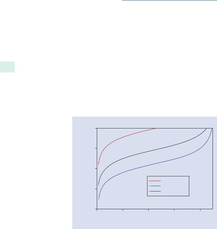
. Fig. 10.2 Plot of secondary electron topographic contrast between two flat surfaces with a difference in tilt angle of 1°, 5°, and 10°
SE contrast between planar surfaces
1
0.1
0.01
0.001
0.0001
0
Secondary electron topographic contrast
Dq = 10 degrees
Dq = 1 degree
Dq = 5 degrees
20 |
40 |
60 |
80 |
Average tilt angle (degrees)