

- •Preface
- •Imaging Microscopic Features
- •Measuring the Crystal Structure
- •References
- •Contents
- •1.4 Simulating the Effects of Elastic Scattering: Monte Carlo Calculations
- •What Are the Main Features of the Beam Electron Interaction Volume?
- •How Does the Interaction Volume Change with Composition?
- •How Does the Interaction Volume Change with Incident Beam Energy?
- •How Does the Interaction Volume Change with Specimen Tilt?
- •1.5 A Range Equation To Estimate the Size of the Interaction Volume
- •References
- •2: Backscattered Electrons
- •2.1 Origin
- •2.2.1 BSE Response to Specimen Composition (η vs. Atomic Number, Z)
- •SEM Image Contrast with BSE: “Atomic Number Contrast”
- •SEM Image Contrast: “BSE Topographic Contrast—Number Effects”
- •2.2.3 Angular Distribution of Backscattering
- •Beam Incident at an Acute Angle to the Specimen Surface (Specimen Tilt > 0°)
- •SEM Image Contrast: “BSE Topographic Contrast—Trajectory Effects”
- •2.2.4 Spatial Distribution of Backscattering
- •Depth Distribution of Backscattering
- •Radial Distribution of Backscattered Electrons
- •2.3 Summary
- •References
- •3: Secondary Electrons
- •3.1 Origin
- •3.2 Energy Distribution
- •3.3 Escape Depth of Secondary Electrons
- •3.8 Spatial Characteristics of Secondary Electrons
- •References
- •4: X-Rays
- •4.1 Overview
- •4.2 Characteristic X-Rays
- •4.2.1 Origin
- •4.2.2 Fluorescence Yield
- •4.2.3 X-Ray Families
- •4.2.4 X-Ray Nomenclature
- •4.2.6 Characteristic X-Ray Intensity
- •Isolated Atoms
- •X-Ray Production in Thin Foils
- •X-Ray Intensity Emitted from Thick, Solid Specimens
- •4.3 X-Ray Continuum (bremsstrahlung)
- •4.3.1 X-Ray Continuum Intensity
- •4.3.3 Range of X-ray Production
- •4.4 X-Ray Absorption
- •4.5 X-Ray Fluorescence
- •References
- •5.1 Electron Beam Parameters
- •5.2 Electron Optical Parameters
- •5.2.1 Beam Energy
- •Landing Energy
- •5.2.2 Beam Diameter
- •5.2.3 Beam Current
- •5.2.4 Beam Current Density
- •5.2.5 Beam Convergence Angle, α
- •5.2.6 Beam Solid Angle
- •5.2.7 Electron Optical Brightness, β
- •Brightness Equation
- •5.2.8 Focus
- •Astigmatism
- •5.3 SEM Imaging Modes
- •5.3.1 High Depth-of-Field Mode
- •5.3.2 High-Current Mode
- •5.3.3 Resolution Mode
- •5.3.4 Low-Voltage Mode
- •5.4 Electron Detectors
- •5.4.1 Important Properties of BSE and SE for Detector Design and Operation
- •Abundance
- •Angular Distribution
- •Kinetic Energy Response
- •5.4.2 Detector Characteristics
- •Angular Measures for Electron Detectors
- •Elevation (Take-Off) Angle, ψ, and Azimuthal Angle, ζ
- •Solid Angle, Ω
- •Energy Response
- •Bandwidth
- •5.4.3 Common Types of Electron Detectors
- •Backscattered Electrons
- •Passive Detectors
- •Scintillation Detectors
- •Semiconductor BSE Detectors
- •5.4.4 Secondary Electron Detectors
- •Everhart–Thornley Detector
- •Through-the-Lens (TTL) Electron Detectors
- •TTL SE Detector
- •TTL BSE Detector
- •Measuring the DQE: BSE Semiconductor Detector
- •References
- •6: Image Formation
- •6.1 Image Construction by Scanning Action
- •6.2 Magnification
- •6.3 Making Dimensional Measurements With the SEM: How Big Is That Feature?
- •Using a Calibrated Structure in ImageJ-Fiji
- •6.4 Image Defects
- •6.4.1 Projection Distortion (Foreshortening)
- •6.4.2 Image Defocusing (Blurring)
- •6.5 Making Measurements on Surfaces With Arbitrary Topography: Stereomicroscopy
- •6.5.1 Qualitative Stereomicroscopy
- •Fixed beam, Specimen Position Altered
- •Fixed Specimen, Beam Incidence Angle Changed
- •6.5.2 Quantitative Stereomicroscopy
- •Measuring a Simple Vertical Displacement
- •References
- •7: SEM Image Interpretation
- •7.1 Information in SEM Images
- •7.2.2 Calculating Atomic Number Contrast
- •Establishing a Robust Light-Optical Analogy
- •Getting It Wrong: Breaking the Light-Optical Analogy of the Everhart–Thornley (Positive Bias) Detector
- •Deconstructing the SEM/E–T Image of Topography
- •SUM Mode (A + B)
- •DIFFERENCE Mode (A−B)
- •References
- •References
- •9: Image Defects
- •9.1 Charging
- •9.1.1 What Is Specimen Charging?
- •9.1.3 Techniques to Control Charging Artifacts (High Vacuum Instruments)
- •Observing Uncoated Specimens
- •Coating an Insulating Specimen for Charge Dissipation
- •Choosing the Coating for Imaging Morphology
- •9.2 Radiation Damage
- •9.3 Contamination
- •References
- •10: High Resolution Imaging
- •10.2 Instrumentation Considerations
- •10.4.1 SE Range Effects Produce Bright Edges (Isolated Edges)
- •10.4.4 Too Much of a Good Thing: The Bright Edge Effect Hinders Locating the True Position of an Edge for Critical Dimension Metrology
- •10.5.1 Beam Energy Strategies
- •Low Beam Energy Strategy
- •High Beam Energy Strategy
- •Making More SE1: Apply a Thin High-δ Metal Coating
- •Making Fewer BSEs, SE2, and SE3 by Eliminating Bulk Scattering From the Substrate
- •10.6 Factors That Hinder Achieving High Resolution
- •10.6.2 Pathological Specimen Behavior
- •Contamination
- •Instabilities
- •References
- •11: Low Beam Energy SEM
- •11.3 Selecting the Beam Energy to Control the Spatial Sampling of Imaging Signals
- •11.3.1 Low Beam Energy for High Lateral Resolution SEM
- •11.3.2 Low Beam Energy for High Depth Resolution SEM
- •11.3.3 Extremely Low Beam Energy Imaging
- •References
- •12.1.1 Stable Electron Source Operation
- •12.1.2 Maintaining Beam Integrity
- •12.1.4 Minimizing Contamination
- •12.3.1 Control of Specimen Charging
- •12.5 VPSEM Image Resolution
- •References
- •13: ImageJ and Fiji
- •13.1 The ImageJ Universe
- •13.2 Fiji
- •13.3 Plugins
- •13.4 Where to Learn More
- •References
- •14: SEM Imaging Checklist
- •14.1.1 Conducting or Semiconducting Specimens
- •14.1.2 Insulating Specimens
- •14.2 Electron Signals Available
- •14.2.1 Beam Electron Range
- •14.2.2 Backscattered Electrons
- •14.2.3 Secondary Electrons
- •14.3 Selecting the Electron Detector
- •14.3.2 Backscattered Electron Detectors
- •14.3.3 “Through-the-Lens” Detectors
- •14.4 Selecting the Beam Energy for SEM Imaging
- •14.4.4 High Resolution SEM Imaging
- •Strategy 1
- •Strategy 2
- •14.5 Selecting the Beam Current
- •14.5.1 High Resolution Imaging
- •14.5.2 Low Contrast Features Require High Beam Current and/or Long Frame Time to Establish Visibility
- •14.6 Image Presentation
- •14.6.1 “Live” Display Adjustments
- •14.6.2 Post-Collection Processing
- •14.7 Image Interpretation
- •14.7.1 Observer’s Point of View
- •14.7.3 Contrast Encoding
- •14.8.1 VPSEM Advantages
- •14.8.2 VPSEM Disadvantages
- •15: SEM Case Studies
- •15.1 Case Study: How High Is That Feature Relative to Another?
- •15.2 Revealing Shallow Surface Relief
- •16.1.2 Minor Artifacts: The Si-Escape Peak
- •16.1.3 Minor Artifacts: Coincidence Peaks
- •16.1.4 Minor Artifacts: Si Absorption Edge and Si Internal Fluorescence Peak
- •16.2 “Best Practices” for Electron-Excited EDS Operation
- •16.2.1 Operation of the EDS System
- •Choosing the EDS Time Constant (Resolution and Throughput)
- •Choosing the Solid Angle of the EDS
- •Selecting a Beam Current for an Acceptable Level of System Dead-Time
- •16.3.1 Detector Geometry
- •16.3.2 Process Time
- •16.3.3 Optimal Working Distance
- •16.3.4 Detector Orientation
- •16.3.5 Count Rate Linearity
- •16.3.6 Energy Calibration Linearity
- •16.3.7 Other Items
- •16.3.8 Setting Up a Quality Control Program
- •Using the QC Tools Within DTSA-II
- •Creating a QC Project
- •Linearity of Output Count Rate with Live-Time Dose
- •Resolution and Peak Position Stability with Count Rate
- •Solid Angle for Low X-ray Flux
- •Maximizing Throughput at Moderate Resolution
- •References
- •17: DTSA-II EDS Software
- •17.1 Getting Started With NIST DTSA-II
- •17.1.1 Motivation
- •17.1.2 Platform
- •17.1.3 Overview
- •17.1.4 Design
- •Simulation
- •Quantification
- •Experiment Design
- •Modeled Detectors (. Fig. 17.1)
- •Window Type (. Fig. 17.2)
- •The Optimal Working Distance (. Figs. 17.3 and 17.4)
- •Elevation Angle
- •Sample-to-Detector Distance
- •Detector Area
- •Crystal Thickness
- •Number of Channels, Energy Scale, and Zero Offset
- •Resolution at Mn Kα (Approximate)
- •Azimuthal Angle
- •Gold Layer, Aluminum Layer, Nickel Layer
- •Dead Layer
- •Zero Strobe Discriminator (. Figs. 17.7 and 17.8)
- •Material Editor Dialog (. Figs. 17.9, 17.10, 17.11, 17.12, 17.13, and 17.14)
- •17.2.1 Introduction
- •17.2.2 Monte Carlo Simulation
- •17.2.4 Optional Tables
- •References
- •18: Qualitative Elemental Analysis by Energy Dispersive X-Ray Spectrometry
- •18.1 Quality Assurance Issues for Qualitative Analysis: EDS Calibration
- •18.2 Principles of Qualitative EDS Analysis
- •Exciting Characteristic X-Rays
- •Fluorescence Yield
- •X-ray Absorption
- •Si Escape Peak
- •Coincidence Peaks
- •18.3 Performing Manual Qualitative Analysis
- •Beam Energy
- •Choosing the EDS Resolution (Detector Time Constant)
- •Obtaining Adequate Counts
- •18.4.1 Employ the Available Software Tools
- •18.4.3 Lower Photon Energy Region
- •18.4.5 Checking Your Work
- •18.5 A Worked Example of Manual Peak Identification
- •References
- •19.1 What Is a k-ratio?
- •19.3 Sets of k-ratios
- •19.5 The Analytical Total
- •19.6 Normalization
- •19.7.1 Oxygen by Assumed Stoichiometry
- •19.7.3 Element by Difference
- •19.8 Ways of Reporting Composition
- •19.8.1 Mass Fraction
- •19.8.2 Atomic Fraction
- •19.8.3 Stoichiometry
- •19.8.4 Oxide Fractions
- •Example Calculations
- •19.9 The Accuracy of Quantitative Electron-Excited X-ray Microanalysis
- •19.9.1 Standards-Based k-ratio Protocol
- •19.9.2 “Standardless Analysis”
- •19.10 Appendix
- •19.10.1 The Need for Matrix Corrections To Achieve Quantitative Analysis
- •19.10.2 The Physical Origin of Matrix Effects
- •19.10.3 ZAF Factors in Microanalysis
- •X-ray Generation With Depth, φ(ρz)
- •X-ray Absorption Effect, A
- •X-ray Fluorescence, F
- •References
- •20.2 Instrumentation Requirements
- •20.2.1 Choosing the EDS Parameters
- •EDS Spectrum Channel Energy Width and Spectrum Energy Span
- •EDS Time Constant (Resolution and Throughput)
- •EDS Calibration
- •EDS Solid Angle
- •20.2.2 Choosing the Beam Energy, E0
- •20.2.3 Measuring the Beam Current
- •20.2.4 Choosing the Beam Current
- •Optimizing Analysis Strategy
- •20.3.4 Ba-Ti Interference in BaTiSi3O9
- •20.4 The Need for an Iterative Qualitative and Quantitative Analysis Strategy
- •20.4.2 Analysis of a Stainless Steel
- •20.5 Is the Specimen Homogeneous?
- •20.6 Beam-Sensitive Specimens
- •20.6.1 Alkali Element Migration
- •20.6.2 Materials Subject to Mass Loss During Electron Bombardment—the Marshall-Hall Method
- •Thin Section Analysis
- •Bulk Biological and Organic Specimens
- •References
- •21: Trace Analysis by SEM/EDS
- •21.1 Limits of Detection for SEM/EDS Microanalysis
- •21.2.1 Estimating CDL from a Trace or Minor Constituent from Measuring a Known Standard
- •21.2.2 Estimating CDL After Determination of a Minor or Trace Constituent with Severe Peak Interference from a Major Constituent
- •21.3 Measurements of Trace Constituents by Electron-Excited Energy Dispersive X-ray Spectrometry
- •The Inevitable Physics of Remote Excitation Within the Specimen: Secondary Fluorescence Beyond the Electron Interaction Volume
- •Simulation of Long-Range Secondary X-ray Fluorescence
- •NIST DTSA II Simulation: Vertical Interface Between Two Regions of Different Composition in a Flat Bulk Target
- •NIST DTSA II Simulation: Cubic Particle Embedded in a Bulk Matrix
- •21.5 Summary
- •References
- •22.1.2 Low Beam Energy Analysis Range
- •22.2 Advantage of Low Beam Energy X-Ray Microanalysis
- •22.2.1 Improved Spatial Resolution
- •22.3 Challenges and Limitations of Low Beam Energy X-Ray Microanalysis
- •22.3.1 Reduced Access to Elements
- •22.3.3 At Low Beam Energy, Almost Everything Is Found To Be Layered
- •Analysis of Surface Contamination
- •References
- •23: Analysis of Specimens with Special Geometry: Irregular Bulk Objects and Particles
- •23.2.1 No Chemical Etching
- •23.3 Consequences of Attempting Analysis of Bulk Materials With Rough Surfaces
- •23.4.1 The Raw Analytical Total
- •23.4.2 The Shape of the EDS Spectrum
- •23.5 Best Practices for Analysis of Rough Bulk Samples
- •23.6 Particle Analysis
- •Particle Sample Preparation: Bulk Substrate
- •The Importance of Beam Placement
- •Overscanning
- •“Particle Mass Effect”
- •“Particle Absorption Effect”
- •The Analytical Total Reveals the Impact of Particle Effects
- •Does Overscanning Help?
- •23.6.6 Peak-to-Background (P/B) Method
- •Specimen Geometry Severely Affects the k-ratio, but Not the P/B
- •Using the P/B Correspondence
- •23.7 Summary
- •References
- •24: Compositional Mapping
- •24.2 X-Ray Spectrum Imaging
- •24.2.1 Utilizing XSI Datacubes
- •24.2.2 Derived Spectra
- •SUM Spectrum
- •MAXIMUM PIXEL Spectrum
- •24.3 Quantitative Compositional Mapping
- •24.4 Strategy for XSI Elemental Mapping Data Collection
- •24.4.1 Choosing the EDS Dead-Time
- •24.4.2 Choosing the Pixel Density
- •24.4.3 Choosing the Pixel Dwell Time
- •“Flash Mapping”
- •High Count Mapping
- •References
- •25.1 Gas Scattering Effects in the VPSEM
- •25.1.1 Why Doesn’t the EDS Collimator Exclude the Remote Skirt X-Rays?
- •25.2 What Can Be Done To Minimize gas Scattering in VPSEM?
- •25.2.2 Favorable Sample Characteristics
- •Particle Analysis
- •25.2.3 Unfavorable Sample Characteristics
- •References
- •26.1 Instrumentation
- •26.1.2 EDS Detector
- •26.1.3 Probe Current Measurement Device
- •Direct Measurement: Using a Faraday Cup and Picoammeter
- •A Faraday Cup
- •Electrically Isolated Stage
- •Indirect Measurement: Using a Calibration Spectrum
- •26.1.4 Conductive Coating
- •26.2 Sample Preparation
- •26.2.1 Standard Materials
- •26.2.2 Peak Reference Materials
- •26.3 Initial Set-Up
- •26.3.1 Calibrating the EDS Detector
- •Selecting a Pulse Process Time Constant
- •Energy Calibration
- •Quality Control
- •Sample Orientation
- •Detector Position
- •Probe Current
- •26.4 Collecting Data
- •26.4.1 Exploratory Spectrum
- •26.4.2 Experiment Optimization
- •26.4.3 Selecting Standards
- •26.4.4 Reference Spectra
- •26.4.5 Collecting Standards
- •26.4.6 Collecting Peak-Fitting References
- •26.5 Data Analysis
- •26.5.2 Quantification
- •26.6 Quality Check
- •Reference
- •27.2 Case Study: Aluminum Wire Failures in Residential Wiring
- •References
- •28: Cathodoluminescence
- •28.1 Origin
- •28.2 Measuring Cathodoluminescence
- •28.3 Applications of CL
- •28.3.1 Geology
- •Carbonado Diamond
- •Ancient Impact Zircons
- •28.3.2 Materials Science
- •Semiconductors
- •Lead-Acid Battery Plate Reactions
- •28.3.3 Organic Compounds
- •References
- •29.1.1 Single Crystals
- •29.1.2 Polycrystalline Materials
- •29.1.3 Conditions for Detecting Electron Channeling Contrast
- •Specimen Preparation
- •Instrument Conditions
- •29.2.1 Origin of EBSD Patterns
- •29.2.2 Cameras for EBSD Pattern Detection
- •29.2.3 EBSD Spatial Resolution
- •29.2.5 Steps in Typical EBSD Measurements
- •Sample Preparation for EBSD
- •Align Sample in the SEM
- •Check for EBSD Patterns
- •Adjust SEM and Select EBSD Map Parameters
- •Run the Automated Map
- •29.2.6 Display of the Acquired Data
- •29.2.7 Other Map Components
- •29.2.10 Application Example
- •Application of EBSD To Understand Meteorite Formation
- •29.2.11 Summary
- •Specimen Considerations
- •EBSD Detector
- •Selection of Candidate Crystallographic Phases
- •Microscope Operating Conditions and Pattern Optimization
- •Selection of EBSD Acquisition Parameters
- •Collect the Orientation Map
- •References
- •30.1 Introduction
- •30.2 Ion–Solid Interactions
- •30.3 Focused Ion Beam Systems
- •30.5 Preparation of Samples for SEM
- •30.5.1 Cross-Section Preparation
- •30.5.2 FIB Sample Preparation for 3D Techniques and Imaging
- •30.6 Summary
- •References
- •31: Ion Beam Microscopy
- •31.1 What Is So Useful About Ions?
- •31.2 Generating Ion Beams
- •31.3 Signal Generation in the HIM
- •31.5 Patterning with Ion Beams
- •31.7 Chemical Microanalysis with Ion Beams
- •References
- •Appendix
- •A Database of Electron–Solid Interactions
- •A Database of Electron–Solid Interactions
- •Introduction
- •Backscattered Electrons
- •Secondary Yields
- •Stopping Powers
- •X-ray Ionization Cross Sections
- •Conclusions
- •References
- •Index
- •Reference List
- •Index
\216 Chapter 16 · Energy Dispersive X-ray Spectrometry: Physical Principles and User-Selected Parameters
Counts
Counts
18 000
16 000
14 000
12 000
10 000
8 000
6 000
4 000
2 000
0
0
18 000
16 000
14 000
12 000
10 000
8 000
6 000
4 000
2 000
0
0
Cu_20kV9.95nA300s
Cu
E0 = 20 keV
500 1 000 1 500 2 000 2 500 Photon energy (eV)
Cu_20kV9.95nA300s
Residual[Cu_20kV9.95nA300s]
500 |
1 000 |
1 500 |
2 000 |
2 500 |
|
|
Photon energy (eV) |
|
|
|
. Fig. 16.8 Cu at E0 = 20 keV. The artifact Si peak is a combination of |
support grid and the Si detector dead-layer, and subsequent Si X-ray |
16 |
the Si K-absorption edge and the Si internal fluorescence peak (peak |
emission |
fitting in lower spectrum) created by absorption of X-rays in the Si |
|
|
|
|
|
peak-like structure. The absorption of X-rays by the Si grid and Si dead-layer ionizes Si atoms and subsequently results in the emission of Si K-shell X-rays, which contribute a false Si peak to the spectrum. In the example for a copper target shown in . Fig. 16.8, the apparent level of Si contributed by the internal fluorescence artifact is approximately 0.002 mass fraction.
16.2\ “Best Practices” for Electron-Excited EDS Operation
While modern EDS systems are well supported by computer automation, there remain parameters whose selection is the responsibility of the user.
16.2.1\ Operation of the EDS System
Before commencing any EDS microanalysis campaign, the analyst should follow an established checklist with careful attention to the measurement science of EDS operation. To establish the basis for quantitative analysis, the EDS parameters must be chosen consistently, especially if the analyst wishes to use archived spectra to serve as standards.
Choosing the EDS Time Constant (Resolution and Throughput)
The EDS amplifier time constant (a generic term which may be locally known as “shaping time,” “processing time,” “resolution,” “count rate range,” “1–6,” etc.) should be checked. There are usually at least two settings, one that optimizes resolution
16.2 · “Best Practices” for Electron-Excited EDS Operation
(at the cost of X-ray throughput) and one that optimizes throughput (at the cost of resolution). Confirming the desired choice of the time constant is critical for consistent recording of spectra, especially if the analyst is using archived spectra to serve as standards for quantitative analysis. This is especially important when the EDS system is in a multi-user environment, since the previous user may have altered this parameter.
Channel Width andNumber
The energy width of the histogram bins is typically chosen as 5, 10, or 20 eV. The bin energy width determines how many bins will define an X-ray peak. Since the peak width is a function of photon energy, as described by Eq. (16.2), decreasing from approximately 129 eV at Mn K-L3 (5.895 keV) to approximately 50 eV FWHM for C K-L2 (0.282 keV), a selection of a 5-eV bin width is a useful choice to optimize peak fitting since this choice will provide 10 channels across C
K-L2. The number of bins that comprise the spectrum multiplied by the bin width gives the energy span. It is useful to capture the complete energy spectrum from a threshold of 0.1 keV to the incident beam energy, E0. Thus, to span 0–20 keV with 5 eV bins requires 4096 channels.
Choosing the Solid Angle of the EDS
The solid angle Ω of a detector with an active area A at a distance r from the specimen is
W = A / r2 |
\ |
(16.4) |
|
|
217 |
|
16 |
|
|
|
If the EDS is mounted on a translatable slide that can alter the detector-to-specimen distance, then the user must select a specific value for this distance for consistency with archived standard spectra if these are to be used in quantitative analysis procedures. Because of the exponent on the distance parameter r in Eq. (16.4), a small error in r propagates to a much larger error in the solid angle and a proportional deviation in the measured intensity.
Selecting a Beam Current for an Acceptable Level of System Dead-Time
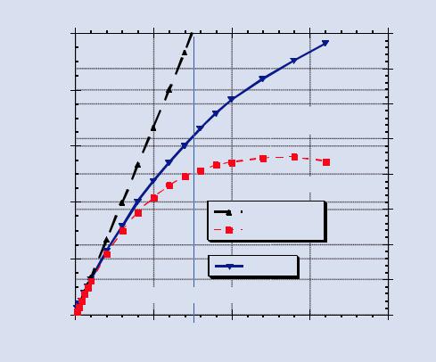
X-rays are generated randomly in time with an average rate determined by the flux of electrons striking the specimen, thus scaling with the incident beam current. As discussed above, the EDS system can measure only one X-ray photon at a time, so that it is effectively unavailable if another photon arrives while the system is “busy” measuring the first photon.
Depending on the separation in the time of arrival of the second photon, the anti-coincidence function will exclude the second photon, but if the measurement of the first photon is not sufficiently advanced, both photons will be excluded from the measurement and effectively lost. Due to this photon loss, the output count rate (OCR) in counts/second of the detector will always be less than the input count rate (ICR). The relation between the OCR and ICR is shown in . Fig. 16.9 for a four-detector SDD-EDS. An automatic correction function measures the time increments when the detector is busy processing photons, and to compensate for possible photon loss during this “dead-time,” additional time is added at the conclusion of the user-specified measurement time so that all
. Fig. 16.9 Output count rate versus input count rate for a fourdetector SDD-EDS
Quad SDD (medium peaking time)
1,000,000 |
|
|
|
|
80 |
|
|
Mn |
|
|
|
|
|
OCR |
E0 = 20 keV |
|
|
|
70 |
|
|
SDD 470 ns |
|
|
|
|
|
|
|
|
|
|
|
|
800,000 |
shaping |
|
|
|
|
|
time |
|
|
|
|
|
|
|
|
|
|
60 |
|
|
|
|
|
Single SDD |
|
|
|
|
|
|
|
|
|
|
|
|
|
Maximum = 130 kcps |
|
|
|
600,000 |
|
|
550 kHz |
|
50 |
|
|
|
|
|
|
||
|
|
|
|
|
Deadtime |
|
|
|
|
127.5 eV at MnKα |
40 |
||
|
|
|
|
|||
400,000 |
|
|
|
|
|
|
(c/s)rateCount |
|
|
ICR (c/clock-s) |
30 |
||
|
|
|
OCR (Medium) |
|
|
|
|
|
|
|
|
20 |
|
200,000 |
|
|
Deadtime |
|
|
|
|
|
|
|
|
|
|
|
|
|
|
|
10 |
|
|
Single SDD chip: maximum output ~ 130 kHz |
|
|
|
||
0 |
|
|
|
|
0 |
|
0 |
500 kHz |
1MHz |
1.5 MHz |
2 MHz |
2.5 MHz |
|
Input count rate
\218 Chapter 16 · Energy Dispersive X-ray Spectrometry: Physical Principles and User-Selected Parameters
measurements are made on the basis of the same “live-time” so as to achieve constant dose for quantitative measurements. The level of activity of the EDS is reported to the user as a percentage “dead-time”:
Deadtime(%)= (ICR − OCR) / ICR ×100% (16.5) |
||
|
|
\ |
|
|
|
Dead-time increases as the beam current increases. The dead time correction circuit can correct the measurement
time over the full dead-time range to 80 % or higher. (Note that as a component of a quality measurement system, the dead-time correction function should be periodically checked by systematically changing the beam current and comparing the measured X-ray intensity with predicted.) However, as the dead-time increases and the arrival rate of X-rays at the EDS increases, coincidence events become progressively more prominent. This effect is illustrated in
. Fig. 16.10 for a sequence of spectra from a glass with six
Counts
16
Counts
140 000
120 000
100 000
80 000
60 000
40 000
20 000
0
0
14 000
12 000
10 000
8 000
6 000
4 000
2 000
0
0
2O K not NaK
K412
E0 = 20 keV 7% deadtime
2 |
|
|
4 |
6 |
|
|
|
Photon energy (keV) |
|
Coincidence |
|
Coincidence |
||
peaks |
|
|
peaks |
|
SiK+O K 2MgK |
2AlK |
2SiK |
AlK+CaK-L, not V K-L |
-SiKL+CaK-L, not CrK-L |
16DT |
||||
20DT |
|
|
|
|
12DT |
|
|
|
|
10DT |
|
|
|
|
7DT |
|
|
|
|
2 |
|
|
4 |
6 |
|
|
|
Energy (keV) |
|
K412 (mass frac)
O |
0.428 |
Mg |
0.117 |
Al |
0.0491 |
Si |
0.212 |
Ca |
0.109 |
Fe |
0.0774 |
8 |
10 |
K412 (mass frac)
O |
0.428 |
Mg |
0.117 |
Al |
0.0491 |
Si |
0.212 |
Ca |
0.109 |
Fe |
0.0774 |
8 |
10 |
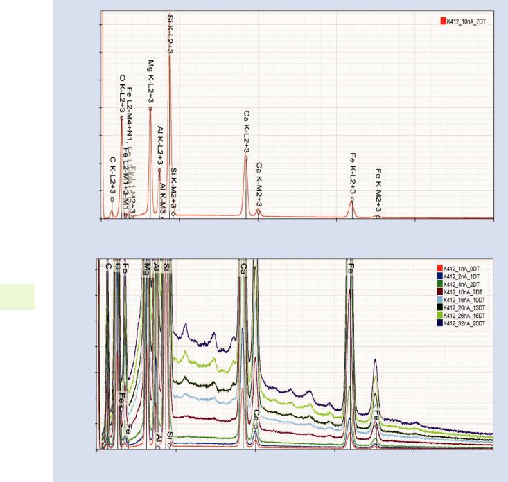
. Fig. 16.10 Development of coincidence peaks as a function of deadtime. NIST Standard Reference Material SRM 470 (Mineral Glasses) K412. (upper) SDD-EDS spectrum at 7 % dead-time showing the characteristic
peaks for O, Mg, Al, Si, Ca, and Fe. (lower) SDD-EDS spectra recorded over arrange of dead-times showing in-growth of coincidence peaks. Note elemental misidentifications that are possible

219 |
16 |
16.3 · Practical Aspects of Ensuring EDS Performance for a Quality Measurement Environment
major constituents (O, Mg, Al, Si, Ca, and Fe) measured at increasing dead-time. The spectra show the in-growth of a series of coincidence peaks as the dead-time increases. With the long pulses of the Si(Li) EDS technology, the pulse inspection function was effective in minimizing coincidence effects to dead-times in the range 20–30 %. There is more vendor-to-vendor variability in SDD-EDS technology. Some vendors provide coincidence detection that will permit dead-times of up to 50 %, while others are restricted to 10 % dead-time. Since there is variability among vendors’ SDD performance, it is useful to perform a measurement to determine the performance characteristic of each detector. See the sidebar for a procedure implementing such a procedure. Regardless of dead-time restrictions, an SDD-EDS is still a factor of 10 or more faster than an Si(Li)-EDS for the same resolution. In summary, as a critical step in establishing a quality measurement strategy, the beam current (for a specific EDS solid angle) should be selected to produce an acceptable rate of coincidence events in the worst-case scenario. This beam current can then be used for all measurements with reasonable expectation that the dead-time will be within acceptable limits.
kSidebar: Protocol for Determining the Optimal Probe Current and Dead-Time
Aluminum produces one of the highest fluxes of X-rays per unit probe current: With the Al K-shell ionization energy of 1.559 keV, a modest beam energy of 15 keV provides an overvoltage of 9.6 for strong excitation. Al K-L2 is of sufficient energy (1.487 keV) that it has low self-absorption, and at this energy the SDD efficiency is also relatively high. The Al K-L2 energy is low enough that this peak is also quite susceptible to coincidence events. Pure aluminum thus makes an ideal sample for testing the coincidence detection performance of a detector and for determining the maximum practical probe current for a given beam energy.
\1.\ Place a mounted, flat, polished sample of pure Al in the SEM chamber at optimal analytical working distance.
\2.\ Mount a Faraday cup with a picoammeter in the SEM chamber.
\3.\ Configure the detector at the desired process time.
\4.\ Configure the SEM at the desired beam energy and an initial probe current. Measure the probe current using the Faraday cup/picoammeter.
\5.\ Collect a spectrum from the pure Al sample with at least 10,000 counts in the Al K peak.
\6.\ Use your vendor’s software (or NIST DTSA-II) to integrate the background-corrected intensity in the Al K peak (E = 1.486 keV).
\7.\ Use your vendor’s software (or NIST DTSA-II) to look for and integrate the background-corrected intensity in the Al K + Al K coincidence peak (E = 2.972 keV).
\8.\ Determine the ratio of the integrated intensity I(Al
K + Al K)/I(Al K). We desire this ratio to be smaller than 0.01 (1 %). In some trace analysis situations, it may desirable to have this ratio less than 0.001 (0.1 %). Setting this limit too low will limit throughput but
setting it too high may make trace element analysis challenging.
\ 9.\ If the ratio is too large, decrease the probe current and re-measure the probe current and the Al spectrum. Re-measure the ratio I(Al K + Al K)/I(Al K).
\10.\ Repeat steps 5–10 until a suitable probe current has been determine.
\11.\ Finally, note the suitable probe current and use it consistently at the beam energy for which it was determined.
16.3\ Practical Aspects of Ensuring EDS
Performance for a Quality
Measurement Environment
The modern energy dispersive X-ray spectrometer is an amazing device capable of measuring the energy of tens of thousands of X-ray events per second. The spectra can be processed to extract measures of composition with a precision of a fraction of a weight-percent. However, this potential will not be realized if the detector is not performing optimally. It is important to ensure that the detector is mounted and configured optimally each time it is used. Some parameters change infrequently and need only be checked when a significant modification is made to the detector or the SEM. Other parameters and performance metrics can change from day-to-day and need to be verified more frequently. The following sections will step through a series of tests in a rationally ordered progression. The initial tests and configuration steps need only be performed occasionally, for example, when the detector is first commissioned or when a significant service event has occurred. Later steps, like ensuring proper calibration, should be performed regularly and a archival record of the results maintained.
16.3.1\ Detector Geometry
In most electron-beam instruments, the EDS detector is mounted on a fixed flange to ensure a consistent sample/ detector geometry with a fixed elevation angle. Almost all modern EDS detectors are mounted in a tubular snout with the crystal mounted at the end of the snout and the face of the active detector element perpendicular to the principle axis of the snout. The principal axis of the snout is oriented in the instrument such that it intersects with the electron beam axis at the “optimal working distance.” This geometry is illustrated in . Fig. 16.11.
Often the detector is mounted on the flange on a sliding mechanism that allows the position of the detector to translate (move in and out) along the axis of the snout. The elevation angle is nominally held fixed during the translation but the distance from the detector crystal changes and along with it the solid angle (Ω) subtended by the detector. The solid

220\ Chapter 16 · Energy Dispersive X-ray Spectrometry: Physical Principles and User-Selected Parameters
. Fig. 16.11 The elevation angle is a fixed property of the instrument/detector
|
|
|
C |
|
|
|
|
|
L |
|
|
|
|
|
Objective |
|
|
|
|
|
lens |
|
|
|
|
|
|
tor |
snout |
|
|
|
|
|
|
Axes |
X |
|
EDS |
detec |
|
|
|
|
|||
Y |
|
Optimal |
|
|
|
|
|
|
|
|
|
Z |
|
working |
ψ: Elevation angle |
|
|
|
distance |
|
|||
Sample
. Fig. 16.12 The solid angle is a function of sample-to-detector distance and the active detector area
16
C
L
Objective
lens
|
Detector |
W |
crystal |
Sample |
Sample-to |
|
|
|
-detector |
|
distance |
angle is illustrated in the . Fig. 16.12. Moving the detector away from the sample is designed to decrease the solid angle but does not change the elevation angle or the optimal working distance.
It is important to be able to maintain a reproducible solid angle through consistent repositioning of the detector. Some slide mechanisms are motorized. Motorized mechanisms should define an “inserted” position and a “retracted”
221 |
16 |
16.3 · Practical Aspects of Ensuring EDS Performance for a Quality Measurement Environment
position, which you should test to ensure that the positioning is reproducible between insertions. Manual mechanisms usually provide a threaded screw with a manual crank to pull the detector in and out. The threaded screw will usually have a pair of interlocking nuts which can be positioned to define a consistent insertion position. The procedure in the sidebar below will allow you to set and maintain a constant solid angle and thus also a consistent detector collection efficiency.
zz Sidebar: Setting a Constant Detector-to-Sample Distance to Maintain Solid Angle
\1.\ Locate the pair of lock nuts on the screw mechanism. Move the lock nuts to the inner most position on the treaded rod.
\2.\ Insert the detector as close to the sample as possible. Ensure that the detector does not touch the interior of the microscope. The detector snout must be electrically isolated (no conductive path) from the interior of the chamber to eliminate noise caused by electrical ground loops.
\3.\ Twist the upper lock nut to limit the motion of the detector towards the sample. Tighten the lower nut to lock the upper nut into position.
\4.\ Test the reproducibility of the insertion point by extracting and inserting the detector and collecting a series of spectra. If the characteristic peak intensities are reproducible (to much better than a fraction of a percent) between insertions, the precision is adequate.
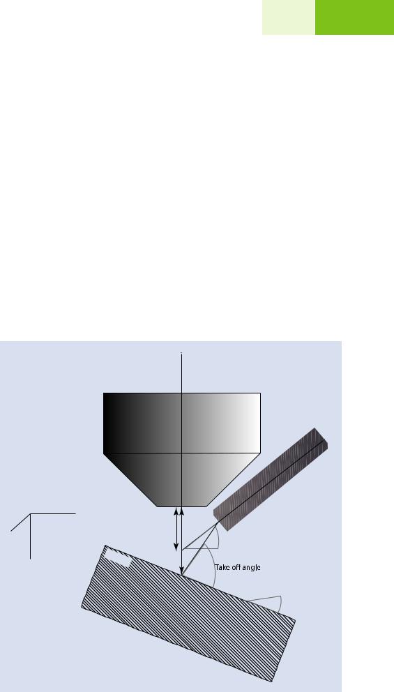
The take-off angle is the angle at which X-rays exit a flat sample in the direction of the detector. For a flat sample mounted perpendicular to the electron beam at the optimal working distance, the take-off angle equals the elevation angle. If the sample is tilted or the sample surface is at a slightly different working distance, then the take-off angle can be computed from the sample tilt, the working distance and the sample-to- detector distance. This is shown in . Fig. 16.13. Often you will hear the terms elevation angle and take-off angle used interchangeably. It is more precise however to think of the elevation angle as being a fixed property of the instrument/ detector geometry and the take-off angle being dependent upon instrument-specimen configuration.
zz Check 1: Verify the Elevation Angle
It is critical that your quantitative analysis software has the correct elevation/take-off angle. Matrix correction algorithms
use the take-off angle to calculate the correct absorption
. Fig. 16.13 The take-off angle is a function of the elevation angle, the sample tilt and the actual working distance
C
L
Objective
lens
Axes X
Y
Optimal |
working |
|
|
distanc |
|
|
|
|
|
|
e |
ψ:
|
tor |
snout |
|
|
|
EDS |
detec |
|
|
|
|
Ac |
|
|
|
tual |
working |
Elevation angle |
|
|
||
|
|
|
|
Z |
Sample |
distance |
|
|
|
||
|
|
|
|
Sample tilt