

- •Preface
- •Imaging Microscopic Features
- •Measuring the Crystal Structure
- •References
- •Contents
- •1.4 Simulating the Effects of Elastic Scattering: Monte Carlo Calculations
- •What Are the Main Features of the Beam Electron Interaction Volume?
- •How Does the Interaction Volume Change with Composition?
- •How Does the Interaction Volume Change with Incident Beam Energy?
- •How Does the Interaction Volume Change with Specimen Tilt?
- •1.5 A Range Equation To Estimate the Size of the Interaction Volume
- •References
- •2: Backscattered Electrons
- •2.1 Origin
- •2.2.1 BSE Response to Specimen Composition (η vs. Atomic Number, Z)
- •SEM Image Contrast with BSE: “Atomic Number Contrast”
- •SEM Image Contrast: “BSE Topographic Contrast—Number Effects”
- •2.2.3 Angular Distribution of Backscattering
- •Beam Incident at an Acute Angle to the Specimen Surface (Specimen Tilt > 0°)
- •SEM Image Contrast: “BSE Topographic Contrast—Trajectory Effects”
- •2.2.4 Spatial Distribution of Backscattering
- •Depth Distribution of Backscattering
- •Radial Distribution of Backscattered Electrons
- •2.3 Summary
- •References
- •3: Secondary Electrons
- •3.1 Origin
- •3.2 Energy Distribution
- •3.3 Escape Depth of Secondary Electrons
- •3.8 Spatial Characteristics of Secondary Electrons
- •References
- •4: X-Rays
- •4.1 Overview
- •4.2 Characteristic X-Rays
- •4.2.1 Origin
- •4.2.2 Fluorescence Yield
- •4.2.3 X-Ray Families
- •4.2.4 X-Ray Nomenclature
- •4.2.6 Characteristic X-Ray Intensity
- •Isolated Atoms
- •X-Ray Production in Thin Foils
- •X-Ray Intensity Emitted from Thick, Solid Specimens
- •4.3 X-Ray Continuum (bremsstrahlung)
- •4.3.1 X-Ray Continuum Intensity
- •4.3.3 Range of X-ray Production
- •4.4 X-Ray Absorption
- •4.5 X-Ray Fluorescence
- •References
- •5.1 Electron Beam Parameters
- •5.2 Electron Optical Parameters
- •5.2.1 Beam Energy
- •Landing Energy
- •5.2.2 Beam Diameter
- •5.2.3 Beam Current
- •5.2.4 Beam Current Density
- •5.2.5 Beam Convergence Angle, α
- •5.2.6 Beam Solid Angle
- •5.2.7 Electron Optical Brightness, β
- •Brightness Equation
- •5.2.8 Focus
- •Astigmatism
- •5.3 SEM Imaging Modes
- •5.3.1 High Depth-of-Field Mode
- •5.3.2 High-Current Mode
- •5.3.3 Resolution Mode
- •5.3.4 Low-Voltage Mode
- •5.4 Electron Detectors
- •5.4.1 Important Properties of BSE and SE for Detector Design and Operation
- •Abundance
- •Angular Distribution
- •Kinetic Energy Response
- •5.4.2 Detector Characteristics
- •Angular Measures for Electron Detectors
- •Elevation (Take-Off) Angle, ψ, and Azimuthal Angle, ζ
- •Solid Angle, Ω
- •Energy Response
- •Bandwidth
- •5.4.3 Common Types of Electron Detectors
- •Backscattered Electrons
- •Passive Detectors
- •Scintillation Detectors
- •Semiconductor BSE Detectors
- •5.4.4 Secondary Electron Detectors
- •Everhart–Thornley Detector
- •Through-the-Lens (TTL) Electron Detectors
- •TTL SE Detector
- •TTL BSE Detector
- •Measuring the DQE: BSE Semiconductor Detector
- •References
- •6: Image Formation
- •6.1 Image Construction by Scanning Action
- •6.2 Magnification
- •6.3 Making Dimensional Measurements With the SEM: How Big Is That Feature?
- •Using a Calibrated Structure in ImageJ-Fiji
- •6.4 Image Defects
- •6.4.1 Projection Distortion (Foreshortening)
- •6.4.2 Image Defocusing (Blurring)
- •6.5 Making Measurements on Surfaces With Arbitrary Topography: Stereomicroscopy
- •6.5.1 Qualitative Stereomicroscopy
- •Fixed beam, Specimen Position Altered
- •Fixed Specimen, Beam Incidence Angle Changed
- •6.5.2 Quantitative Stereomicroscopy
- •Measuring a Simple Vertical Displacement
- •References
- •7: SEM Image Interpretation
- •7.1 Information in SEM Images
- •7.2.2 Calculating Atomic Number Contrast
- •Establishing a Robust Light-Optical Analogy
- •Getting It Wrong: Breaking the Light-Optical Analogy of the Everhart–Thornley (Positive Bias) Detector
- •Deconstructing the SEM/E–T Image of Topography
- •SUM Mode (A + B)
- •DIFFERENCE Mode (A−B)
- •References
- •References
- •9: Image Defects
- •9.1 Charging
- •9.1.1 What Is Specimen Charging?
- •9.1.3 Techniques to Control Charging Artifacts (High Vacuum Instruments)
- •Observing Uncoated Specimens
- •Coating an Insulating Specimen for Charge Dissipation
- •Choosing the Coating for Imaging Morphology
- •9.2 Radiation Damage
- •9.3 Contamination
- •References
- •10: High Resolution Imaging
- •10.2 Instrumentation Considerations
- •10.4.1 SE Range Effects Produce Bright Edges (Isolated Edges)
- •10.4.4 Too Much of a Good Thing: The Bright Edge Effect Hinders Locating the True Position of an Edge for Critical Dimension Metrology
- •10.5.1 Beam Energy Strategies
- •Low Beam Energy Strategy
- •High Beam Energy Strategy
- •Making More SE1: Apply a Thin High-δ Metal Coating
- •Making Fewer BSEs, SE2, and SE3 by Eliminating Bulk Scattering From the Substrate
- •10.6 Factors That Hinder Achieving High Resolution
- •10.6.2 Pathological Specimen Behavior
- •Contamination
- •Instabilities
- •References
- •11: Low Beam Energy SEM
- •11.3 Selecting the Beam Energy to Control the Spatial Sampling of Imaging Signals
- •11.3.1 Low Beam Energy for High Lateral Resolution SEM
- •11.3.2 Low Beam Energy for High Depth Resolution SEM
- •11.3.3 Extremely Low Beam Energy Imaging
- •References
- •12.1.1 Stable Electron Source Operation
- •12.1.2 Maintaining Beam Integrity
- •12.1.4 Minimizing Contamination
- •12.3.1 Control of Specimen Charging
- •12.5 VPSEM Image Resolution
- •References
- •13: ImageJ and Fiji
- •13.1 The ImageJ Universe
- •13.2 Fiji
- •13.3 Plugins
- •13.4 Where to Learn More
- •References
- •14: SEM Imaging Checklist
- •14.1.1 Conducting or Semiconducting Specimens
- •14.1.2 Insulating Specimens
- •14.2 Electron Signals Available
- •14.2.1 Beam Electron Range
- •14.2.2 Backscattered Electrons
- •14.2.3 Secondary Electrons
- •14.3 Selecting the Electron Detector
- •14.3.2 Backscattered Electron Detectors
- •14.3.3 “Through-the-Lens” Detectors
- •14.4 Selecting the Beam Energy for SEM Imaging
- •14.4.4 High Resolution SEM Imaging
- •Strategy 1
- •Strategy 2
- •14.5 Selecting the Beam Current
- •14.5.1 High Resolution Imaging
- •14.5.2 Low Contrast Features Require High Beam Current and/or Long Frame Time to Establish Visibility
- •14.6 Image Presentation
- •14.6.1 “Live” Display Adjustments
- •14.6.2 Post-Collection Processing
- •14.7 Image Interpretation
- •14.7.1 Observer’s Point of View
- •14.7.3 Contrast Encoding
- •14.8.1 VPSEM Advantages
- •14.8.2 VPSEM Disadvantages
- •15: SEM Case Studies
- •15.1 Case Study: How High Is That Feature Relative to Another?
- •15.2 Revealing Shallow Surface Relief
- •16.1.2 Minor Artifacts: The Si-Escape Peak
- •16.1.3 Minor Artifacts: Coincidence Peaks
- •16.1.4 Minor Artifacts: Si Absorption Edge and Si Internal Fluorescence Peak
- •16.2 “Best Practices” for Electron-Excited EDS Operation
- •16.2.1 Operation of the EDS System
- •Choosing the EDS Time Constant (Resolution and Throughput)
- •Choosing the Solid Angle of the EDS
- •Selecting a Beam Current for an Acceptable Level of System Dead-Time
- •16.3.1 Detector Geometry
- •16.3.2 Process Time
- •16.3.3 Optimal Working Distance
- •16.3.4 Detector Orientation
- •16.3.5 Count Rate Linearity
- •16.3.6 Energy Calibration Linearity
- •16.3.7 Other Items
- •16.3.8 Setting Up a Quality Control Program
- •Using the QC Tools Within DTSA-II
- •Creating a QC Project
- •Linearity of Output Count Rate with Live-Time Dose
- •Resolution and Peak Position Stability with Count Rate
- •Solid Angle for Low X-ray Flux
- •Maximizing Throughput at Moderate Resolution
- •References
- •17: DTSA-II EDS Software
- •17.1 Getting Started With NIST DTSA-II
- •17.1.1 Motivation
- •17.1.2 Platform
- •17.1.3 Overview
- •17.1.4 Design
- •Simulation
- •Quantification
- •Experiment Design
- •Modeled Detectors (. Fig. 17.1)
- •Window Type (. Fig. 17.2)
- •The Optimal Working Distance (. Figs. 17.3 and 17.4)
- •Elevation Angle
- •Sample-to-Detector Distance
- •Detector Area
- •Crystal Thickness
- •Number of Channels, Energy Scale, and Zero Offset
- •Resolution at Mn Kα (Approximate)
- •Azimuthal Angle
- •Gold Layer, Aluminum Layer, Nickel Layer
- •Dead Layer
- •Zero Strobe Discriminator (. Figs. 17.7 and 17.8)
- •Material Editor Dialog (. Figs. 17.9, 17.10, 17.11, 17.12, 17.13, and 17.14)
- •17.2.1 Introduction
- •17.2.2 Monte Carlo Simulation
- •17.2.4 Optional Tables
- •References
- •18: Qualitative Elemental Analysis by Energy Dispersive X-Ray Spectrometry
- •18.1 Quality Assurance Issues for Qualitative Analysis: EDS Calibration
- •18.2 Principles of Qualitative EDS Analysis
- •Exciting Characteristic X-Rays
- •Fluorescence Yield
- •X-ray Absorption
- •Si Escape Peak
- •Coincidence Peaks
- •18.3 Performing Manual Qualitative Analysis
- •Beam Energy
- •Choosing the EDS Resolution (Detector Time Constant)
- •Obtaining Adequate Counts
- •18.4.1 Employ the Available Software Tools
- •18.4.3 Lower Photon Energy Region
- •18.4.5 Checking Your Work
- •18.5 A Worked Example of Manual Peak Identification
- •References
- •19.1 What Is a k-ratio?
- •19.3 Sets of k-ratios
- •19.5 The Analytical Total
- •19.6 Normalization
- •19.7.1 Oxygen by Assumed Stoichiometry
- •19.7.3 Element by Difference
- •19.8 Ways of Reporting Composition
- •19.8.1 Mass Fraction
- •19.8.2 Atomic Fraction
- •19.8.3 Stoichiometry
- •19.8.4 Oxide Fractions
- •Example Calculations
- •19.9 The Accuracy of Quantitative Electron-Excited X-ray Microanalysis
- •19.9.1 Standards-Based k-ratio Protocol
- •19.9.2 “Standardless Analysis”
- •19.10 Appendix
- •19.10.1 The Need for Matrix Corrections To Achieve Quantitative Analysis
- •19.10.2 The Physical Origin of Matrix Effects
- •19.10.3 ZAF Factors in Microanalysis
- •X-ray Generation With Depth, φ(ρz)
- •X-ray Absorption Effect, A
- •X-ray Fluorescence, F
- •References
- •20.2 Instrumentation Requirements
- •20.2.1 Choosing the EDS Parameters
- •EDS Spectrum Channel Energy Width and Spectrum Energy Span
- •EDS Time Constant (Resolution and Throughput)
- •EDS Calibration
- •EDS Solid Angle
- •20.2.2 Choosing the Beam Energy, E0
- •20.2.3 Measuring the Beam Current
- •20.2.4 Choosing the Beam Current
- •Optimizing Analysis Strategy
- •20.3.4 Ba-Ti Interference in BaTiSi3O9
- •20.4 The Need for an Iterative Qualitative and Quantitative Analysis Strategy
- •20.4.2 Analysis of a Stainless Steel
- •20.5 Is the Specimen Homogeneous?
- •20.6 Beam-Sensitive Specimens
- •20.6.1 Alkali Element Migration
- •20.6.2 Materials Subject to Mass Loss During Electron Bombardment—the Marshall-Hall Method
- •Thin Section Analysis
- •Bulk Biological and Organic Specimens
- •References
- •21: Trace Analysis by SEM/EDS
- •21.1 Limits of Detection for SEM/EDS Microanalysis
- •21.2.1 Estimating CDL from a Trace or Minor Constituent from Measuring a Known Standard
- •21.2.2 Estimating CDL After Determination of a Minor or Trace Constituent with Severe Peak Interference from a Major Constituent
- •21.3 Measurements of Trace Constituents by Electron-Excited Energy Dispersive X-ray Spectrometry
- •The Inevitable Physics of Remote Excitation Within the Specimen: Secondary Fluorescence Beyond the Electron Interaction Volume
- •Simulation of Long-Range Secondary X-ray Fluorescence
- •NIST DTSA II Simulation: Vertical Interface Between Two Regions of Different Composition in a Flat Bulk Target
- •NIST DTSA II Simulation: Cubic Particle Embedded in a Bulk Matrix
- •21.5 Summary
- •References
- •22.1.2 Low Beam Energy Analysis Range
- •22.2 Advantage of Low Beam Energy X-Ray Microanalysis
- •22.2.1 Improved Spatial Resolution
- •22.3 Challenges and Limitations of Low Beam Energy X-Ray Microanalysis
- •22.3.1 Reduced Access to Elements
- •22.3.3 At Low Beam Energy, Almost Everything Is Found To Be Layered
- •Analysis of Surface Contamination
- •References
- •23: Analysis of Specimens with Special Geometry: Irregular Bulk Objects and Particles
- •23.2.1 No Chemical Etching
- •23.3 Consequences of Attempting Analysis of Bulk Materials With Rough Surfaces
- •23.4.1 The Raw Analytical Total
- •23.4.2 The Shape of the EDS Spectrum
- •23.5 Best Practices for Analysis of Rough Bulk Samples
- •23.6 Particle Analysis
- •Particle Sample Preparation: Bulk Substrate
- •The Importance of Beam Placement
- •Overscanning
- •“Particle Mass Effect”
- •“Particle Absorption Effect”
- •The Analytical Total Reveals the Impact of Particle Effects
- •Does Overscanning Help?
- •23.6.6 Peak-to-Background (P/B) Method
- •Specimen Geometry Severely Affects the k-ratio, but Not the P/B
- •Using the P/B Correspondence
- •23.7 Summary
- •References
- •24: Compositional Mapping
- •24.2 X-Ray Spectrum Imaging
- •24.2.1 Utilizing XSI Datacubes
- •24.2.2 Derived Spectra
- •SUM Spectrum
- •MAXIMUM PIXEL Spectrum
- •24.3 Quantitative Compositional Mapping
- •24.4 Strategy for XSI Elemental Mapping Data Collection
- •24.4.1 Choosing the EDS Dead-Time
- •24.4.2 Choosing the Pixel Density
- •24.4.3 Choosing the Pixel Dwell Time
- •“Flash Mapping”
- •High Count Mapping
- •References
- •25.1 Gas Scattering Effects in the VPSEM
- •25.1.1 Why Doesn’t the EDS Collimator Exclude the Remote Skirt X-Rays?
- •25.2 What Can Be Done To Minimize gas Scattering in VPSEM?
- •25.2.2 Favorable Sample Characteristics
- •Particle Analysis
- •25.2.3 Unfavorable Sample Characteristics
- •References
- •26.1 Instrumentation
- •26.1.2 EDS Detector
- •26.1.3 Probe Current Measurement Device
- •Direct Measurement: Using a Faraday Cup and Picoammeter
- •A Faraday Cup
- •Electrically Isolated Stage
- •Indirect Measurement: Using a Calibration Spectrum
- •26.1.4 Conductive Coating
- •26.2 Sample Preparation
- •26.2.1 Standard Materials
- •26.2.2 Peak Reference Materials
- •26.3 Initial Set-Up
- •26.3.1 Calibrating the EDS Detector
- •Selecting a Pulse Process Time Constant
- •Energy Calibration
- •Quality Control
- •Sample Orientation
- •Detector Position
- •Probe Current
- •26.4 Collecting Data
- •26.4.1 Exploratory Spectrum
- •26.4.2 Experiment Optimization
- •26.4.3 Selecting Standards
- •26.4.4 Reference Spectra
- •26.4.5 Collecting Standards
- •26.4.6 Collecting Peak-Fitting References
- •26.5 Data Analysis
- •26.5.2 Quantification
- •26.6 Quality Check
- •Reference
- •27.2 Case Study: Aluminum Wire Failures in Residential Wiring
- •References
- •28: Cathodoluminescence
- •28.1 Origin
- •28.2 Measuring Cathodoluminescence
- •28.3 Applications of CL
- •28.3.1 Geology
- •Carbonado Diamond
- •Ancient Impact Zircons
- •28.3.2 Materials Science
- •Semiconductors
- •Lead-Acid Battery Plate Reactions
- •28.3.3 Organic Compounds
- •References
- •29.1.1 Single Crystals
- •29.1.2 Polycrystalline Materials
- •29.1.3 Conditions for Detecting Electron Channeling Contrast
- •Specimen Preparation
- •Instrument Conditions
- •29.2.1 Origin of EBSD Patterns
- •29.2.2 Cameras for EBSD Pattern Detection
- •29.2.3 EBSD Spatial Resolution
- •29.2.5 Steps in Typical EBSD Measurements
- •Sample Preparation for EBSD
- •Align Sample in the SEM
- •Check for EBSD Patterns
- •Adjust SEM and Select EBSD Map Parameters
- •Run the Automated Map
- •29.2.6 Display of the Acquired Data
- •29.2.7 Other Map Components
- •29.2.10 Application Example
- •Application of EBSD To Understand Meteorite Formation
- •29.2.11 Summary
- •Specimen Considerations
- •EBSD Detector
- •Selection of Candidate Crystallographic Phases
- •Microscope Operating Conditions and Pattern Optimization
- •Selection of EBSD Acquisition Parameters
- •Collect the Orientation Map
- •References
- •30.1 Introduction
- •30.2 Ion–Solid Interactions
- •30.3 Focused Ion Beam Systems
- •30.5 Preparation of Samples for SEM
- •30.5.1 Cross-Section Preparation
- •30.5.2 FIB Sample Preparation for 3D Techniques and Imaging
- •30.6 Summary
- •References
- •31: Ion Beam Microscopy
- •31.1 What Is So Useful About Ions?
- •31.2 Generating Ion Beams
- •31.3 Signal Generation in the HIM
- •31.5 Patterning with Ion Beams
- •31.7 Chemical Microanalysis with Ion Beams
- •References
- •Appendix
- •A Database of Electron–Solid Interactions
- •A Database of Electron–Solid Interactions
- •Introduction
- •Backscattered Electrons
- •Secondary Yields
- •Stopping Powers
- •X-ray Ionization Cross Sections
- •Conclusions
- •References
- •Index
- •Reference List
- •Index
References
a
Counts
489 |
|
28 |
|
|
|
b
4000
c
3500
3000
2500
2000
1500
1000
500
0
300 |
350 |
400 |
450 |
500 |
550 |
600 |
650 |
700 |
750 |
800 |
|
|
|
|
|
nm |
|
|
|
|
|
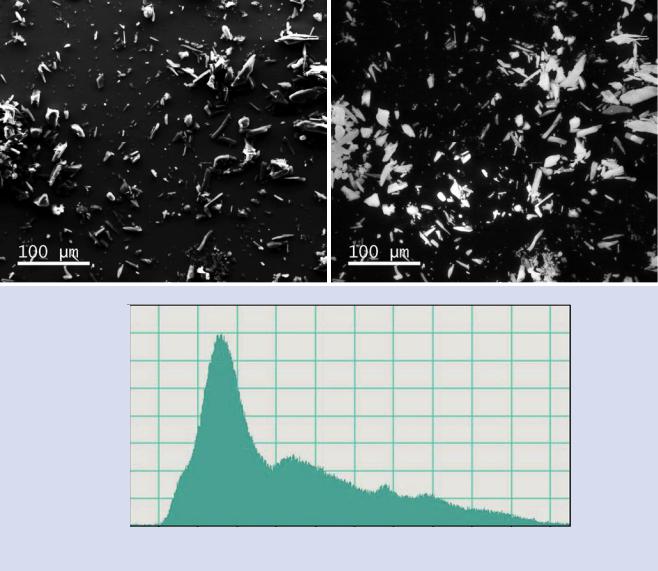
. Fig. 28.12 Acetaminophen, E0 = 20 keV: a SEM SE image; b panchromatic CL image; c CL spectrum (Example courtesy of S. Wight, NIST)
28.3.3\ Organic Compounds |
|
References |
|
|
|
Despite the general vulnerability of organic compounds to radiation damage under electron bombardment, some organic compounds can be examined with CL spectrometry.
. Figure 28.12 shows an SEM SE image and a panchromatic CL image of acetaminophen (paracetamol, N-(4-hydroxyphenyl) ethanamide N-(4-hydroxyphenyl)acetamide) along with a CL spectrum showing broad CL bands.
Magee C, Teles G, Vicenzi E, Taylor W, Heaney P (2016) Uranium irradiation history of carbonado diamond; implications for Paleoarchean oxidation in the São Francisco craton (South America). Geology 44. doi: 10.1130/G37749.1
Zanetti M, Wittman A, Carpenter PK, Joliff BL, Vicenzi E, Nemchin A, Timms N (2015) Using EPMA, Raman LS, Hyperspetcral CL, SIMS, and EBSD to study impact meltinduced decomposition of zircon. Microsc Microanal 21:S3 1447–1448

491 |
|
29 |
|
|
|
Characterizing Crystalline
Materials in the SEM
29.1\ Imaging Crystalline Materials with Electron Channeling Contrast – 492
29.1.1\ Single Crystals – 492
29.1.2\ Polycrystalline Materials – 494
29.1.3\ Conditions for Detecting Electron Channeling Contrast – 496
29.2\ Electron Backscatter Diffraction in the Scanning Electron Microscope – 496
29.2.1\ Origin of EBSD Patterns – 498
29.2.2\ Cameras for EBSD Pattern Detection – 499 29.2.3\ EBSD Spatial Resolution – 499
29.2.4\ How Does a Modern EBSD System Index Patterns – 501 29.2.5\ Steps in Typical EBSD Measurements – 502
29.2.6\ Display of the Acquired Data – 505 29.2.7\ Other Map Components – 508
29.2.8\ Dangers and Practice of “Cleaning” EBSD Data – 508 29.2.9\ Transmission Kikuchi Diffraction in the SEM – 509 29.2.10\ Application Example – 510
29.2.11\ Summary – 513
29.2.12\ Electron Backscatter Diffraction Checklist – 513
References – 514
© Springer Science+Business Media LLC 2018
J. Goldstein et al., Scanning Electron Microscopy and X-Ray Microanalysis, https://doi.org/10.1007/978-1-4939-6676-9_29
\492 Chapter 29 · Characterizing Crystalline Materials in the SEM
While amorphous substances such as glass are encountered both in natural and artificial materials, most inorganic materials are found to be crystalline on some scale, ranging from sub-nanometer to centimeter or larger. A crystal consists of a regular arrangement of atoms, the so-called “unit cell,” which is repeated in a twoor three-dimensional pattern. In the previous discussion of electron beam–specimen interactions, the crystal structure of the target was not considered as a variable in the electron range equation or in the Monte Carlo electron trajectory simulation. To a first order, the crystal structure
29 does not have a strong effect on the electron–specimen interactions. However, through the phenomenon of channeling of charged particles through the crystal lattice, crystal orientation can cause small perturbations in the total electron backscattering coefficient that can be utilized to image crystallographic microstructure through the mechanism designated “electron channeling contrast,” also referred to as
“orientation contrast” (Newbury et al. 1986). The characteristics of a crystal (e.g., interplanar angles and spacings) and its relative orientation can be determined through diffraction of the high-energy backscattered electrons (BSE) to form “electron backscatter diffraction patterns (EBSD).
29.1\ Imaging Crystalline Materials
with Electron Channeling Contrast
29.1.1\ Single Crystals
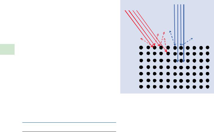
The regular arrangement of atoms in crystalline solids can influence the backscattering of electrons because of the regular three-dimensional variations in atomic density in the crystal compared to those same atoms placed in the near random three-dimensional distribution of an amorphous solid. If a well-collimated (i.e., highly parallel) electron beam is directed at a crystal array of atoms along a series of different directions, the density of atoms that the beam encounters will vary with the crystal orientation, as shown in the simple schematic of . Fig. 29.1. A sense of this effect can be obtained by manual manipulation of a macroscopic, three-dimensional ball-and-stick model of a crystal. For certain orientations of the model, the observer can see through the “atoms” along the open gaps between the planes in the model. In a real solid, the atoms are tightly packed, limited in their approach by the repulsive interaction of their atomic shells. The “channels” in reality are regions of the crystal where the atomic packing creates lower charge density with which the beam electrons will interact more weakly. When the beam is aligned with the channels, a small fraction of the beam electrons penetrate more deeply into the crystal before beginning to scatter. For beam electrons that start scattering deeper in the crystal, the probability that they will return to the surface as backscattered electrons is reduced compared to the amorphous target case, and so the measured backscatter coefficient is lowered compared to the average value from the amorphous target.
. Fig. 29.1 Schematic illustration of the channeling effect: the atomic area density that the beam encounters depends on its orientation relative to the crystal
For other crystal orientations where denser atom packing is found, the beam electrons begin to scatter immediately at the surface, increasing the backscatter coefficient relative to the amorphous target case. As seen in the Monte Carlo simulation of an amorphous target, the elastic scattering of beam electrons rapidly randomizes their trajectories out of their initially well-collimated condition, reducing and eventually eliminating sensitivity to channeling in the crystal. For a bulk target, the modulation of the backscatter coefficient between the maximum and minimum channeling case is small, typically only about a 2–5 % difference. Nevertheless, this crystallographic or electron channeling contrast can be used to form SEM images that contain information about the important class of crystalline materials.
To determine the likelihood of electron channeling, the properties of the electron beam (i.e., its energy, E, or equivalently, wavelength, λ) are related to the critical crystal property, namely the spacing of the atomic planes, d, through the Bragg diffraction relation:
nλ =2d sinθB \ |
(29.1) |
where n is the integer order of diffraction (n = 1, 2, 3, etc.). Equation 29.1 defines a special beam incidence angle relative to a particular set of the crystal planes with spacing d (referred to as the “Bragg angle,” θB) at which the channeling condition changes sharply from weak to strong as the beam incidence angle increases relative to that particular set of crystal planes. Since a real crystal contains many different possible sets of atom planes, the degree of channeling
29.1 · Imaging Crystalline Materials with Electron Channeling Contrast
encountered for an arbitrary orientation of the beam to the crystal is actually the sum of the contributions of many planes. Generally, these contributions tend to cancel giving the amorphous average backscattering except when the Bragg condition for a certain set of planes dominates the mix, giving rise to a sharp change in the channeling condition. What is the magnitude of Bragg angles for typical SEM beam and target conditions? Consider an incident beam of E0 = 15 keV, where the electron wavelength, λe is given by the de Broglie equation:
λe =h/p \ |
(29.2a) |
where h is Planck’s constant and p is the momentum (m0v). In terms of beam energy, the wavelength is given by
λ (nm)=1.226 / E0.5 |
(1+ 0.979E − 6 E)0.5 |
(29.2b) |
|
e |
|
|
\ |
|
|
|
|
where E is expressed in eV (Hirsch et al. 1965).
At 15 keV, λe = 0.00994 nm. If this 15 keV-beam is directed at a crystal of silicon, which has a diamond-cubic crystal lattice with a fundamental cube dimension of a = 0.543 nm, the series of possible “allowed” Bragg angles (expressed in the “Miller indices” [hkl] which designate the crystal planes) is given in . Table 29.1.
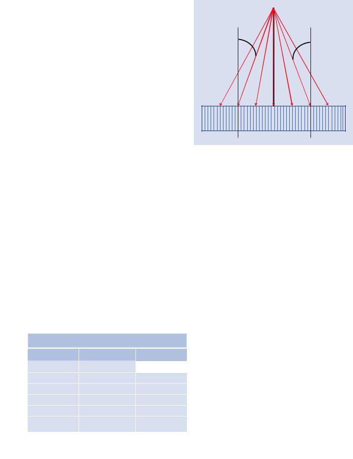
We can directly image the effects of crystallographic channeling on the total backscattered electron intensity for the special case of a large single crystal viewed with a large scanned area (i.e., low magnification). As shown schematically in . Fig. 29.2, the act of image scanning not only moves the beam laterally in x- and y-directions, but at each beam position the angle of the beam relative to the surface normal changes. For a 10-mm working distance from the scan rocking point, a scan excursion of 2 mm in width causes the beam incidence angle to change by ±12° across the field. As seen in
. Table 29.1, the allowed Bragg angles for a 15-keV electron beam striking Si have values of a fraction of a degree to a few degrees, so that a scan angle of ±12° will certainly cause the beam to pass through the Bragg condition for at least some of
. Table 29.1 Bragg angles for Si with E0 = 15 keV
Planes (hkl) |
Spacing (nm) |
θB (degrees) |
111 |
0.314 |
0.908 |
|
|
|
220 |
0.192 |
1.48 |
311 |
0.164 |
1.74 |
400 |
0.136 |
2.10 |
422 |
0.111 |
2.57 |
511 |
0.105 |
2.72 |
493 |
|
29 |
|
|
|
–qB |
qB |
. Fig. 29.2 Wide field (“low magnification”) image scanning produces sufficiently large changes in the scan incidence angle to pass through the Bragg conditions for the particular set of crystal planes. Note that the Bragg condition is satisfied in positive and negative going angles, giving rise to two sharp changes in contrast
the crystal planes. A large area image created at E0 = 15 keV by scanning a flat, topographically featureless silicon crys- tal—prepared with the surface nearly parallel to the (001) plane—is shown in . Fig. 29.3. The image consists of a pattern of bands, each running parallel to a particular crystal plane, creating a so-called electron channeling pattern (Coates 1967). The channeling effect appears as this series of prominent bands that span the crystal because the intersection of the crystal planes with the surface defines a linear trace, and the Bragg condition is satisfied along lines parallel to this trace where the scan angle relative to the planes equals the Bragg angle, ±θB. “Higher order” Bragg angles (n = 2, 3, 4, etc., with the specific integers that appear depending on “allowed reflections”) are satisfied as a series of progressively fainter lines parallel to the central bands, which can be seen in . Fig. 29.3 (b) for the family of {220} type bands. Note that it is appropriate to apply both a dimensional marker and an angular marker to this image. When the scanned area is decreased, that is, the magnification is increased, the range of the angular scan is reduced, and consequently, the bands on the display appear to widen and the angular extent of the electron channeling pattern decreases, as shown in
. Fig. 29.4a, b. If the magnification is made high enough and the angular range is sufficiently reduced, the beam will scan through such a small angle that the observer will see the center of the pattern swell to eventually fill the image with a single gray level. Effectively, the crystal presents a single atomic density that restricts the channeling effect to a single intensity value.