

- •Preface
- •Imaging Microscopic Features
- •Measuring the Crystal Structure
- •References
- •Contents
- •1.4 Simulating the Effects of Elastic Scattering: Monte Carlo Calculations
- •What Are the Main Features of the Beam Electron Interaction Volume?
- •How Does the Interaction Volume Change with Composition?
- •How Does the Interaction Volume Change with Incident Beam Energy?
- •How Does the Interaction Volume Change with Specimen Tilt?
- •1.5 A Range Equation To Estimate the Size of the Interaction Volume
- •References
- •2: Backscattered Electrons
- •2.1 Origin
- •2.2.1 BSE Response to Specimen Composition (η vs. Atomic Number, Z)
- •SEM Image Contrast with BSE: “Atomic Number Contrast”
- •SEM Image Contrast: “BSE Topographic Contrast—Number Effects”
- •2.2.3 Angular Distribution of Backscattering
- •Beam Incident at an Acute Angle to the Specimen Surface (Specimen Tilt > 0°)
- •SEM Image Contrast: “BSE Topographic Contrast—Trajectory Effects”
- •2.2.4 Spatial Distribution of Backscattering
- •Depth Distribution of Backscattering
- •Radial Distribution of Backscattered Electrons
- •2.3 Summary
- •References
- •3: Secondary Electrons
- •3.1 Origin
- •3.2 Energy Distribution
- •3.3 Escape Depth of Secondary Electrons
- •3.8 Spatial Characteristics of Secondary Electrons
- •References
- •4: X-Rays
- •4.1 Overview
- •4.2 Characteristic X-Rays
- •4.2.1 Origin
- •4.2.2 Fluorescence Yield
- •4.2.3 X-Ray Families
- •4.2.4 X-Ray Nomenclature
- •4.2.6 Characteristic X-Ray Intensity
- •Isolated Atoms
- •X-Ray Production in Thin Foils
- •X-Ray Intensity Emitted from Thick, Solid Specimens
- •4.3 X-Ray Continuum (bremsstrahlung)
- •4.3.1 X-Ray Continuum Intensity
- •4.3.3 Range of X-ray Production
- •4.4 X-Ray Absorption
- •4.5 X-Ray Fluorescence
- •References
- •5.1 Electron Beam Parameters
- •5.2 Electron Optical Parameters
- •5.2.1 Beam Energy
- •Landing Energy
- •5.2.2 Beam Diameter
- •5.2.3 Beam Current
- •5.2.4 Beam Current Density
- •5.2.5 Beam Convergence Angle, α
- •5.2.6 Beam Solid Angle
- •5.2.7 Electron Optical Brightness, β
- •Brightness Equation
- •5.2.8 Focus
- •Astigmatism
- •5.3 SEM Imaging Modes
- •5.3.1 High Depth-of-Field Mode
- •5.3.2 High-Current Mode
- •5.3.3 Resolution Mode
- •5.3.4 Low-Voltage Mode
- •5.4 Electron Detectors
- •5.4.1 Important Properties of BSE and SE for Detector Design and Operation
- •Abundance
- •Angular Distribution
- •Kinetic Energy Response
- •5.4.2 Detector Characteristics
- •Angular Measures for Electron Detectors
- •Elevation (Take-Off) Angle, ψ, and Azimuthal Angle, ζ
- •Solid Angle, Ω
- •Energy Response
- •Bandwidth
- •5.4.3 Common Types of Electron Detectors
- •Backscattered Electrons
- •Passive Detectors
- •Scintillation Detectors
- •Semiconductor BSE Detectors
- •5.4.4 Secondary Electron Detectors
- •Everhart–Thornley Detector
- •Through-the-Lens (TTL) Electron Detectors
- •TTL SE Detector
- •TTL BSE Detector
- •Measuring the DQE: BSE Semiconductor Detector
- •References
- •6: Image Formation
- •6.1 Image Construction by Scanning Action
- •6.2 Magnification
- •6.3 Making Dimensional Measurements With the SEM: How Big Is That Feature?
- •Using a Calibrated Structure in ImageJ-Fiji
- •6.4 Image Defects
- •6.4.1 Projection Distortion (Foreshortening)
- •6.4.2 Image Defocusing (Blurring)
- •6.5 Making Measurements on Surfaces With Arbitrary Topography: Stereomicroscopy
- •6.5.1 Qualitative Stereomicroscopy
- •Fixed beam, Specimen Position Altered
- •Fixed Specimen, Beam Incidence Angle Changed
- •6.5.2 Quantitative Stereomicroscopy
- •Measuring a Simple Vertical Displacement
- •References
- •7: SEM Image Interpretation
- •7.1 Information in SEM Images
- •7.2.2 Calculating Atomic Number Contrast
- •Establishing a Robust Light-Optical Analogy
- •Getting It Wrong: Breaking the Light-Optical Analogy of the Everhart–Thornley (Positive Bias) Detector
- •Deconstructing the SEM/E–T Image of Topography
- •SUM Mode (A + B)
- •DIFFERENCE Mode (A−B)
- •References
- •References
- •9: Image Defects
- •9.1 Charging
- •9.1.1 What Is Specimen Charging?
- •9.1.3 Techniques to Control Charging Artifacts (High Vacuum Instruments)
- •Observing Uncoated Specimens
- •Coating an Insulating Specimen for Charge Dissipation
- •Choosing the Coating for Imaging Morphology
- •9.2 Radiation Damage
- •9.3 Contamination
- •References
- •10: High Resolution Imaging
- •10.2 Instrumentation Considerations
- •10.4.1 SE Range Effects Produce Bright Edges (Isolated Edges)
- •10.4.4 Too Much of a Good Thing: The Bright Edge Effect Hinders Locating the True Position of an Edge for Critical Dimension Metrology
- •10.5.1 Beam Energy Strategies
- •Low Beam Energy Strategy
- •High Beam Energy Strategy
- •Making More SE1: Apply a Thin High-δ Metal Coating
- •Making Fewer BSEs, SE2, and SE3 by Eliminating Bulk Scattering From the Substrate
- •10.6 Factors That Hinder Achieving High Resolution
- •10.6.2 Pathological Specimen Behavior
- •Contamination
- •Instabilities
- •References
- •11: Low Beam Energy SEM
- •11.3 Selecting the Beam Energy to Control the Spatial Sampling of Imaging Signals
- •11.3.1 Low Beam Energy for High Lateral Resolution SEM
- •11.3.2 Low Beam Energy for High Depth Resolution SEM
- •11.3.3 Extremely Low Beam Energy Imaging
- •References
- •12.1.1 Stable Electron Source Operation
- •12.1.2 Maintaining Beam Integrity
- •12.1.4 Minimizing Contamination
- •12.3.1 Control of Specimen Charging
- •12.5 VPSEM Image Resolution
- •References
- •13: ImageJ and Fiji
- •13.1 The ImageJ Universe
- •13.2 Fiji
- •13.3 Plugins
- •13.4 Where to Learn More
- •References
- •14: SEM Imaging Checklist
- •14.1.1 Conducting or Semiconducting Specimens
- •14.1.2 Insulating Specimens
- •14.2 Electron Signals Available
- •14.2.1 Beam Electron Range
- •14.2.2 Backscattered Electrons
- •14.2.3 Secondary Electrons
- •14.3 Selecting the Electron Detector
- •14.3.2 Backscattered Electron Detectors
- •14.3.3 “Through-the-Lens” Detectors
- •14.4 Selecting the Beam Energy for SEM Imaging
- •14.4.4 High Resolution SEM Imaging
- •Strategy 1
- •Strategy 2
- •14.5 Selecting the Beam Current
- •14.5.1 High Resolution Imaging
- •14.5.2 Low Contrast Features Require High Beam Current and/or Long Frame Time to Establish Visibility
- •14.6 Image Presentation
- •14.6.1 “Live” Display Adjustments
- •14.6.2 Post-Collection Processing
- •14.7 Image Interpretation
- •14.7.1 Observer’s Point of View
- •14.7.3 Contrast Encoding
- •14.8.1 VPSEM Advantages
- •14.8.2 VPSEM Disadvantages
- •15: SEM Case Studies
- •15.1 Case Study: How High Is That Feature Relative to Another?
- •15.2 Revealing Shallow Surface Relief
- •16.1.2 Minor Artifacts: The Si-Escape Peak
- •16.1.3 Minor Artifacts: Coincidence Peaks
- •16.1.4 Minor Artifacts: Si Absorption Edge and Si Internal Fluorescence Peak
- •16.2 “Best Practices” for Electron-Excited EDS Operation
- •16.2.1 Operation of the EDS System
- •Choosing the EDS Time Constant (Resolution and Throughput)
- •Choosing the Solid Angle of the EDS
- •Selecting a Beam Current for an Acceptable Level of System Dead-Time
- •16.3.1 Detector Geometry
- •16.3.2 Process Time
- •16.3.3 Optimal Working Distance
- •16.3.4 Detector Orientation
- •16.3.5 Count Rate Linearity
- •16.3.6 Energy Calibration Linearity
- •16.3.7 Other Items
- •16.3.8 Setting Up a Quality Control Program
- •Using the QC Tools Within DTSA-II
- •Creating a QC Project
- •Linearity of Output Count Rate with Live-Time Dose
- •Resolution and Peak Position Stability with Count Rate
- •Solid Angle for Low X-ray Flux
- •Maximizing Throughput at Moderate Resolution
- •References
- •17: DTSA-II EDS Software
- •17.1 Getting Started With NIST DTSA-II
- •17.1.1 Motivation
- •17.1.2 Platform
- •17.1.3 Overview
- •17.1.4 Design
- •Simulation
- •Quantification
- •Experiment Design
- •Modeled Detectors (. Fig. 17.1)
- •Window Type (. Fig. 17.2)
- •The Optimal Working Distance (. Figs. 17.3 and 17.4)
- •Elevation Angle
- •Sample-to-Detector Distance
- •Detector Area
- •Crystal Thickness
- •Number of Channels, Energy Scale, and Zero Offset
- •Resolution at Mn Kα (Approximate)
- •Azimuthal Angle
- •Gold Layer, Aluminum Layer, Nickel Layer
- •Dead Layer
- •Zero Strobe Discriminator (. Figs. 17.7 and 17.8)
- •Material Editor Dialog (. Figs. 17.9, 17.10, 17.11, 17.12, 17.13, and 17.14)
- •17.2.1 Introduction
- •17.2.2 Monte Carlo Simulation
- •17.2.4 Optional Tables
- •References
- •18: Qualitative Elemental Analysis by Energy Dispersive X-Ray Spectrometry
- •18.1 Quality Assurance Issues for Qualitative Analysis: EDS Calibration
- •18.2 Principles of Qualitative EDS Analysis
- •Exciting Characteristic X-Rays
- •Fluorescence Yield
- •X-ray Absorption
- •Si Escape Peak
- •Coincidence Peaks
- •18.3 Performing Manual Qualitative Analysis
- •Beam Energy
- •Choosing the EDS Resolution (Detector Time Constant)
- •Obtaining Adequate Counts
- •18.4.1 Employ the Available Software Tools
- •18.4.3 Lower Photon Energy Region
- •18.4.5 Checking Your Work
- •18.5 A Worked Example of Manual Peak Identification
- •References
- •19.1 What Is a k-ratio?
- •19.3 Sets of k-ratios
- •19.5 The Analytical Total
- •19.6 Normalization
- •19.7.1 Oxygen by Assumed Stoichiometry
- •19.7.3 Element by Difference
- •19.8 Ways of Reporting Composition
- •19.8.1 Mass Fraction
- •19.8.2 Atomic Fraction
- •19.8.3 Stoichiometry
- •19.8.4 Oxide Fractions
- •Example Calculations
- •19.9 The Accuracy of Quantitative Electron-Excited X-ray Microanalysis
- •19.9.1 Standards-Based k-ratio Protocol
- •19.9.2 “Standardless Analysis”
- •19.10 Appendix
- •19.10.1 The Need for Matrix Corrections To Achieve Quantitative Analysis
- •19.10.2 The Physical Origin of Matrix Effects
- •19.10.3 ZAF Factors in Microanalysis
- •X-ray Generation With Depth, φ(ρz)
- •X-ray Absorption Effect, A
- •X-ray Fluorescence, F
- •References
- •20.2 Instrumentation Requirements
- •20.2.1 Choosing the EDS Parameters
- •EDS Spectrum Channel Energy Width and Spectrum Energy Span
- •EDS Time Constant (Resolution and Throughput)
- •EDS Calibration
- •EDS Solid Angle
- •20.2.2 Choosing the Beam Energy, E0
- •20.2.3 Measuring the Beam Current
- •20.2.4 Choosing the Beam Current
- •Optimizing Analysis Strategy
- •20.3.4 Ba-Ti Interference in BaTiSi3O9
- •20.4 The Need for an Iterative Qualitative and Quantitative Analysis Strategy
- •20.4.2 Analysis of a Stainless Steel
- •20.5 Is the Specimen Homogeneous?
- •20.6 Beam-Sensitive Specimens
- •20.6.1 Alkali Element Migration
- •20.6.2 Materials Subject to Mass Loss During Electron Bombardment—the Marshall-Hall Method
- •Thin Section Analysis
- •Bulk Biological and Organic Specimens
- •References
- •21: Trace Analysis by SEM/EDS
- •21.1 Limits of Detection for SEM/EDS Microanalysis
- •21.2.1 Estimating CDL from a Trace or Minor Constituent from Measuring a Known Standard
- •21.2.2 Estimating CDL After Determination of a Minor or Trace Constituent with Severe Peak Interference from a Major Constituent
- •21.3 Measurements of Trace Constituents by Electron-Excited Energy Dispersive X-ray Spectrometry
- •The Inevitable Physics of Remote Excitation Within the Specimen: Secondary Fluorescence Beyond the Electron Interaction Volume
- •Simulation of Long-Range Secondary X-ray Fluorescence
- •NIST DTSA II Simulation: Vertical Interface Between Two Regions of Different Composition in a Flat Bulk Target
- •NIST DTSA II Simulation: Cubic Particle Embedded in a Bulk Matrix
- •21.5 Summary
- •References
- •22.1.2 Low Beam Energy Analysis Range
- •22.2 Advantage of Low Beam Energy X-Ray Microanalysis
- •22.2.1 Improved Spatial Resolution
- •22.3 Challenges and Limitations of Low Beam Energy X-Ray Microanalysis
- •22.3.1 Reduced Access to Elements
- •22.3.3 At Low Beam Energy, Almost Everything Is Found To Be Layered
- •Analysis of Surface Contamination
- •References
- •23: Analysis of Specimens with Special Geometry: Irregular Bulk Objects and Particles
- •23.2.1 No Chemical Etching
- •23.3 Consequences of Attempting Analysis of Bulk Materials With Rough Surfaces
- •23.4.1 The Raw Analytical Total
- •23.4.2 The Shape of the EDS Spectrum
- •23.5 Best Practices for Analysis of Rough Bulk Samples
- •23.6 Particle Analysis
- •Particle Sample Preparation: Bulk Substrate
- •The Importance of Beam Placement
- •Overscanning
- •“Particle Mass Effect”
- •“Particle Absorption Effect”
- •The Analytical Total Reveals the Impact of Particle Effects
- •Does Overscanning Help?
- •23.6.6 Peak-to-Background (P/B) Method
- •Specimen Geometry Severely Affects the k-ratio, but Not the P/B
- •Using the P/B Correspondence
- •23.7 Summary
- •References
- •24: Compositional Mapping
- •24.2 X-Ray Spectrum Imaging
- •24.2.1 Utilizing XSI Datacubes
- •24.2.2 Derived Spectra
- •SUM Spectrum
- •MAXIMUM PIXEL Spectrum
- •24.3 Quantitative Compositional Mapping
- •24.4 Strategy for XSI Elemental Mapping Data Collection
- •24.4.1 Choosing the EDS Dead-Time
- •24.4.2 Choosing the Pixel Density
- •24.4.3 Choosing the Pixel Dwell Time
- •“Flash Mapping”
- •High Count Mapping
- •References
- •25.1 Gas Scattering Effects in the VPSEM
- •25.1.1 Why Doesn’t the EDS Collimator Exclude the Remote Skirt X-Rays?
- •25.2 What Can Be Done To Minimize gas Scattering in VPSEM?
- •25.2.2 Favorable Sample Characteristics
- •Particle Analysis
- •25.2.3 Unfavorable Sample Characteristics
- •References
- •26.1 Instrumentation
- •26.1.2 EDS Detector
- •26.1.3 Probe Current Measurement Device
- •Direct Measurement: Using a Faraday Cup and Picoammeter
- •A Faraday Cup
- •Electrically Isolated Stage
- •Indirect Measurement: Using a Calibration Spectrum
- •26.1.4 Conductive Coating
- •26.2 Sample Preparation
- •26.2.1 Standard Materials
- •26.2.2 Peak Reference Materials
- •26.3 Initial Set-Up
- •26.3.1 Calibrating the EDS Detector
- •Selecting a Pulse Process Time Constant
- •Energy Calibration
- •Quality Control
- •Sample Orientation
- •Detector Position
- •Probe Current
- •26.4 Collecting Data
- •26.4.1 Exploratory Spectrum
- •26.4.2 Experiment Optimization
- •26.4.3 Selecting Standards
- •26.4.4 Reference Spectra
- •26.4.5 Collecting Standards
- •26.4.6 Collecting Peak-Fitting References
- •26.5 Data Analysis
- •26.5.2 Quantification
- •26.6 Quality Check
- •Reference
- •27.2 Case Study: Aluminum Wire Failures in Residential Wiring
- •References
- •28: Cathodoluminescence
- •28.1 Origin
- •28.2 Measuring Cathodoluminescence
- •28.3 Applications of CL
- •28.3.1 Geology
- •Carbonado Diamond
- •Ancient Impact Zircons
- •28.3.2 Materials Science
- •Semiconductors
- •Lead-Acid Battery Plate Reactions
- •28.3.3 Organic Compounds
- •References
- •29.1.1 Single Crystals
- •29.1.2 Polycrystalline Materials
- •29.1.3 Conditions for Detecting Electron Channeling Contrast
- •Specimen Preparation
- •Instrument Conditions
- •29.2.1 Origin of EBSD Patterns
- •29.2.2 Cameras for EBSD Pattern Detection
- •29.2.3 EBSD Spatial Resolution
- •29.2.5 Steps in Typical EBSD Measurements
- •Sample Preparation for EBSD
- •Align Sample in the SEM
- •Check for EBSD Patterns
- •Adjust SEM and Select EBSD Map Parameters
- •Run the Automated Map
- •29.2.6 Display of the Acquired Data
- •29.2.7 Other Map Components
- •29.2.10 Application Example
- •Application of EBSD To Understand Meteorite Formation
- •29.2.11 Summary
- •Specimen Considerations
- •EBSD Detector
- •Selection of Candidate Crystallographic Phases
- •Microscope Operating Conditions and Pattern Optimization
- •Selection of EBSD Acquisition Parameters
- •Collect the Orientation Map
- •References
- •30.1 Introduction
- •30.2 Ion–Solid Interactions
- •30.3 Focused Ion Beam Systems
- •30.5 Preparation of Samples for SEM
- •30.5.1 Cross-Section Preparation
- •30.5.2 FIB Sample Preparation for 3D Techniques and Imaging
- •30.6 Summary
- •References
- •31: Ion Beam Microscopy
- •31.1 What Is So Useful About Ions?
- •31.2 Generating Ion Beams
- •31.3 Signal Generation in the HIM
- •31.5 Patterning with Ion Beams
- •31.7 Chemical Microanalysis with Ion Beams
- •References
- •Appendix
- •A Database of Electron–Solid Interactions
- •A Database of Electron–Solid Interactions
- •Introduction
- •Backscattered Electrons
- •Secondary Yields
- •Stopping Powers
- •X-ray Ionization Cross Sections
- •Conclusions
- •References
- •Index
- •Reference List
- •Index
346\ Chapter 21 · Trace Analysis by SEM/EDS
. Table 21.2 Corning Glass A, as synthesized and as analyzed with DTSA-II (E0 = 20 keV) [O by stoichiometry; Na (albite); Ca, P
(fluoroapatite); S (pyrite); K, Cl (KCl); Sr (SrTiO3); Ba aSi2O5); Pb (PbTe); Mg, Al, Si, Ti, Mn, Fe, Co, Cu, Zn, Sn, Sb (pure elements)]
|
As-synthesized |
DTSA-II analysis |
Element |
(mass conc) |
(mass conc) |
|
|
|
O |
0.4407 |
0.4474 (stoich.) |
|
|
|
Na |
0.106 |
0.106 ± 0.0002 |
Mg |
0.0160 |
0.0163 ± 0.0001 |
Al |
0.0053 |
0.0051 ± 0.00005 |
Si |
0.3112 |
0.3171 ± 0.0002 |
P |
0.00057 |
0.0003 ± 0.0001 |
S |
0.0004 |
0.00085 ± 0.0001 |
Cl |
0.00069 |
0.00072 ± 0.00005 |
K |
0.0238 |
0.0237 ± 0.0001 |
Ca |
0.0360 |
0.0341 ± 0.0001 |
Ti |
0.00474 |
0.00485 ± 0.0001 |
Mn |
0.00774 |
0.00768 ± 0.0001 |
Fe |
0.00762 |
0.00717 ± 0.0001 |
Co |
0.00134 |
0.00140 ± 0.0001 |
Cu |
0.00935 |
0.00933 ± 0.0001 |
Zn |
0.00035 |
0.00047 ± 0.0001 |
Sr |
0.00085 |
0.0156 ± 0.0006 |
Sn |
0.0015 |
0.0011 ± 0.0003 |
Sb |
0.0132 |
0.0128 ± 0.0002 |
Ba |
0.00502 |
0.00405 ± 0.0002 |
Pb |
0.00111 |
0.050 ± 0.0001 |
The Inevitable Physics of Remote Excitation Within the Specimen: Secondary Fluorescence Beyond the Electron Interaction Volume
The electron interaction volume contains the region within which characteristic and continuum X-rays are directly excited by the beam electrons. Electron excitation effectively creates a volume source of generated X-rays (characteristic and continuum with energies up to the incident beam energy,
21 E0) embedded in the specimen that propagates out from the interaction volume in all directions. A photon propagating into the specimen will eventually undergo photoelectric absorption which ionizes the absorbing atom, and the subsequent de-excitation of this atom will result in emission of its characteristic X-rays, a process referred to as “secondary fluorescence” to distinguish this source from the “primary
fluorescence” induced directly by the beam electrons. Because the range of X-rays is generally one to two orders of magnitude greater than the range of electrons, depending on the photon energy and the specimen composition, the volume of secondary characteristic generation is much larger than the volume of primary characteristic generation. The range of fluorescence of Fe K-L2,3 by Ni K-L2,3 in a 75wt% Ni-25wt% Fe alloy at E0 = 25 keV is shown in . Fig. 21.5. The electron range is fully contained with a hemisphere of radius 2.5 μm, but a hemisphere of 80 -μm radius is required to capture 99 %
of the secondary fluorescence of Fe K-L2,3 by Ni K-L2,3. For quantification with the ZAF matrix correction protocol, the
secondary fluorescence correction factor, F, corrects the calculated composition for the additional radiation created by secondary fluorescence due to characteristic X-rays. An additional correction, c, is necessary for the continuum- induced secondary fluorescence. The F matrix correction factor is generally small compared to the absorption, A, and atomic number, Z, corrections. For a major constituent, the additional radiation due to secondary fluorescence represents a small perturbation in the apparent concentration, often negligible. However, when a constituent is at the trace level in the electron interaction volume, propagation of the primary characteristic and continuum X-rays into a nearby region of the specimen that is richer in this element will create additional X-rays of the trace element by secondary fluorescence. Because of the wide acceptance area of the EDS, this additional remote source of radiation will still be considered to be part of the spectrum produced at the beam position, possibly severely perturbing the accuracy of the analysis of the trace constituent by elevating the measured concentration above the true concentration. Compensation for this artifact requires careful modeling of the electron and X-ray interactions.
Simulation of Long-Range Secondary X-ray Fluorescence
The Monte Carlo electron trajectory simulation embedded in DTSA-II models the primary electron trajectories and primary X-ray generation, as well as the subsequent propagation of the primary characteristic and continuum X-rays through the target and the generation (and subsequent propagation) of secondary characteristic X-rays. The Monte Carlo menu provides “set-pieces” of analytical interest to predict the significance of secondary fluorescence at the trace level:
NIST DTSA II Simulation: Vertical Interface Between Two Regions of Different Composition in a Flat Bulk Target
. Figure 21.6 shows the simulation of an interface between Cu and NIST SRM470 (K-412 glass) for a beam with an incident energy of 25 keV placed 10 μm from the interface in the Cu region. The map of the distribution of excitation reveals the propagation of X-rays from the original electron
21.3 · Measurements of Trace Constituents by Electron-Excited Energy Dispersive X-ray Spectrometry
a 1000000 |
|
|
|
|
|
|
|
||
|
100 |
000 |
|
|
|
|
|
|
Si |
|
|
|
|
|
|
|
|
||
Counts |
|
|
|
|
|
|
|
|
E0 = 20 keV |
10 000 |
|
|
|
|
|
|
|
||
|
|
|
|
|
|
|
|
||
|
1000 |
|
|
|
|
|
|
|
|
|
|
100 |
|
|
|
|
|
|
|
|
|
0.0 |
1.0 |
2.0 |
3.0 |
4.0 |
5.0 |
6.0 |
7.0 |
|
|
|
|
|
|
|
Photon energy (keV) |
|
|
b 1000000 |
|
|
|
|
|
|
|
||
|
|
|
|
|
Si |
|
|
|
|
|
100 |
000 |
|
|
Cr |
|
|
|
|
|
|
|
Cu |
|
|
|
|
||
|
|
|
|
|
|
|
|
|
|
Counts |
|
|
|
|
E0 = 20 keV |
|
|
|
|
10 |
000 |
|
|
|
|
|
|
|
|
|
|
|
|
|
|
|
|
||
|
1000 |
|
|
|
|
|
|
|
|
|
|
100 |
|
|
|
|
|
|
|
|
|
0.0 |
1.0 |
2.0 |
3.0 |
4.0 |
5.0 |
6.0 |
7.0 |
|
|
|
|
|
|
|
Photon energy (keV) |
|
|
347 |
|
21 |
|
|
|
Si_20kV10nA14%DT
8.0 |
9.0 |
10.0 |
 Si_20kV10nA14%DT
 Cr_20kV10nA9%DT
 Cu_20kV10nA10%DT
8.0 |
9.0 |
10.0 |
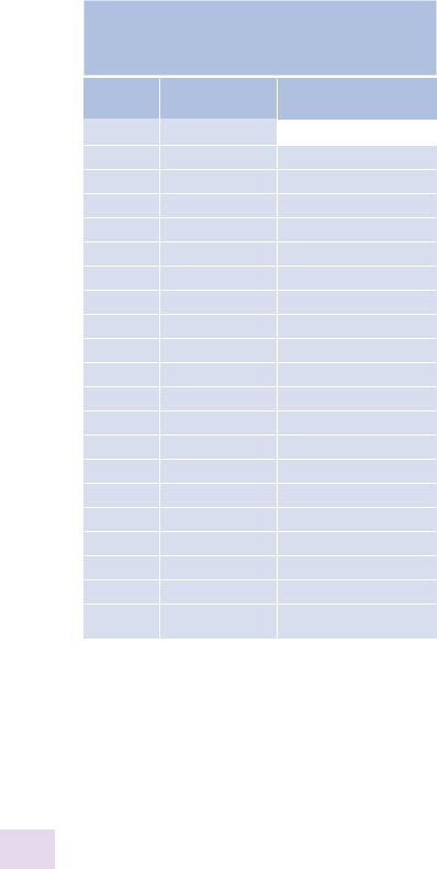
. Fig. 21.4 a SDD-EDS spectrum of Si (20 keV; 1000 nA-s; 0.1–20 keV = 22 million counts) with energy windows defined for Al, Cr, and Cu. b Spectrum for Si with the spectra of Cr and Cu superimposed
. Table 21.3 Estimated limits of detection kDL for a Si
spectrum with 110 million counts (0.1–20 keV)
Element |
kDL |
ZAF |
CDL (mass conc) |
CDL (ppm) |
Al |
0.000115 |
1.12 |
0.000129 |
129 |
|
|
|
|
|
Cr |
0.000133 |
1.01 |
0.000134 |
134 |
Cu |
0.000113 |
1.00 |
0.000113 |
113 |
Range of characteristic-induced fluorescence
Range of direct electron excitation in 75Ni-25Fe at E0 = 25 keV
50%
10 µm |
75% |
|
90% |
||
|
interaction volume into the K412 glass to excite secondary fluorescence. The calculated spectrum shown in . Fig. 21.6 shows the presence of an apparent trace level of Fe (and to a lesser extent, Ca, Si, Al, and Mg) in the Cu, corresponding to k= 0.0028 relative to a pure Fe standard. The Fe k-ratio as a function of beam position in the Cu is also shown in
. Fig. 21.6. Even with the beam placed in the Cu at a distance of 40 μm from the K-412, there is an apparent Fe trace level in the Cu of k = 0.0004, or about 400 ppm.
99%
Ni K-L3 in 75Ni-25Fe
Range of secondary X-ray excitation (characteristic fluorescence)
of Fe K-L3 by Ni K-L3
. Fig. 21.5 Range of secondary fluorescence of FeKα by NiKα in a 75Ni-25Fe alloy at E0 = 25 keV

\348 Chapter 21 · Trace Analysis by SEM/EDS
X-ray counts
300 |
|
280 |
|
260 |
|
240 |
|
220 |
|
200 |
|
180 |
|
160 |
Cu, 10 µm from K412 |
140 |
E0 = 25 keV |
120 |
Fe std |
100 |
|
80 |
|
60 |
|
40 |
|
20 |
|
0 |
|
0 |
1 |
2 |
3 |
4 |
5 |
|
|
|
|
|
|
Photon energy (keV) |
|
|
|
|
|
|
|
0.005 |
|
|
|
|
|
|
0.004 |
|
|
|
|
|
Fe |
0.003 |
|
|
|
|
|
|
|
|
|
|
|
|
k |
0.002 |
|
|
|
|
|
|
|
|
|
|
|
|
|
0.001 |
|
|
20 µm |
|
|
|
0 |
|
10.000 m from a pure |
Fe |
copper/K412 interface. |
MC simulation of bulk Fe |
|
|
Cu |
Fe
Cu
kFe = 0.0028
6 |
7 |
8 |
9 |
10 |
0 |
20 |
40 |
60 |
|
Beam distance from interface ( |
m) |
|
. Fig. 21.6 DTSA-II Monte Carlo calculation of fluorescence across a planar boundary between copper and SRM 470 (K-412 glass). The beam is placed in the copper at various distances from the interface. The spectrum calculated for a beam at 10 μm from the interface shows a small Fe peak, which is ratioed to the intensity calculated for pure
iron, giving kFe = 0.0028. The inset map of the distribution of secondary FeKα X-ray production shows the extent of penetration of characteristic Cu Kα and Cu Kβ and continuum X-rays into the K-412 glass to fluoresce FeKα. Simulations at other distances give the response plotted in the graph
NIST DTSA II Simulation: Cubic Particle Embedded in a Bulk Matrix
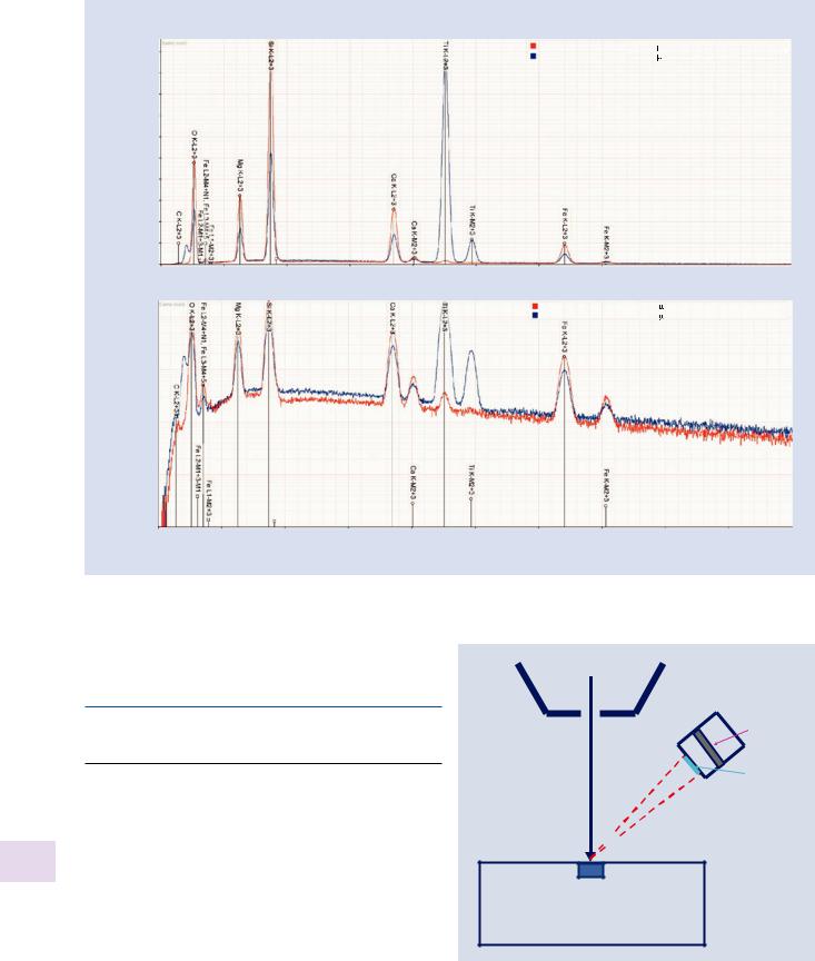
. Figure 21.7(a) shows the results of a simulation of a 1-μm cube of K-411 glass embedded in a titanium matrix and excited with a beam energy of 20 keV. For this size and beam energy, the primary electron trajectories penetrate through the sides and bottom of the cube leading to direct electron excitation of the titanium matrix, which is seen as a major
21 peak in the calculated spectrum. When the cube dimension is increased to 20 μm, the beam trajectories at E0 = 20 keV are contained entirely within the K-411 cube. DTSA-II allows calculations with and without implementing the secondary fluorescence calculation. When secondary fluorescence is not implemented, the calculated spectrum . Fig. 21.7(b)
shows no Ti characteristic X-rays. When secondary fluorescence is included in the simulation, a small Ti peak is observed, corresponding to an artifact trace level k= 0.0007 (700 ppm), demonstrating the long range of the primary X-rays and the creation of a trace level artifact.
When variable pressure SEM operation is considered, the large fraction of gas-scattered electrons creates X-rays from regions up to many millimeters from the beam impact point. Depending on the surroundings, this gas scattering can greatly modify the EDS spectrum from what would originate from the region actually excited by the focused beam.
. Figure 21.7(c) shows this effect as simulated with DTSA II, resulting in a large peak for Ti, which is not present in the specimen but which is located in the surrounding region.
349 |
21 |
21.3 · Measurements of Trace Constituents by Electron-Excited Energy Dispersive X-ray Spectrometry
a
|
15000 |
|
|
Counts |
10 |
000 |
|
|
|
|
|
|
5000 |
|
|
|
|
0 |
|
|
|
|
0 |
b |
20000 |
|
|
|
18000 |
|
|
|
16000 |
|
|
|
14000 |
|
|
Counts |
12000 |
|
|
8 |
000 |
|
|
|
10 |
000 |
|
|
6000 |
|
|
|
4000 |
|
|
|
2000 |
|
|
|
|
0 |
0 |
|
|
|
|
|
10000 |
|
|
|
1000 |
|
|
Counts |
|
100 |
|
|
|
|
|
|
|
10 |
|
|
|
1 |
0 |
Monte Carlo calculation of a cubic inclusion (1 µm edge) of K411 in a Ti matrix at E0 = 20 keV
Fe
O
Mg
1
Si
O
Fe Mg
|
|
5.09 mm x 5.09 mm |
|
|
|
5.09 mm x 5.09 mm |
Si K-M3 |
Ti K-L3 |
|
2 mm |
SiK |
TiKa |
|
|
|
|||||
|
|
|
|
|
|
|
|
|
|
|
|
|
1.21E-3 |
|
Emission |
|
8.95E-3 |
|
|
Emission |
|
|
|
|
|
Si K-M3 |
|
|
|
|
Ti K-L3 |
|
|
|
|
Si |
|
|
|
|
|
|
Ti |
|
|
|
|
|
|
|
|
Ca |
Ti |
|
|
|
|||
|
|
|
|
|
|
|
|
Fe |
|
||
|
|
|
|
|
|
|
|
|
|
|
|
|
|
|
|
|
Ca |
|
|
|
Fe |
|
|
|
|
|
|
|
|
|
|
|
|
|
|
|
|
|
|
|
|
|
|
Photon energy (keV) |
|
|
|
2 |
3 |
4 |
5 |
6 |
7 |
|
|||||
|
|
|
|
|
Photon energy (keV) |
|
|
|
|||
|
|
|
|
|
|
|
|
|
Noisy[MC simulatoin of a 20.000 |
m |
|
|
|
|
|
|
|
|
|
|
cubic inclusion of K411 in Ti] #1 |
|
|
|
|
|
|
|
|
|
|
|
Noisy[MC simulatoin of a 20.000 |
m |
|
|
|
|
|
|
|
|
|
|
cubic inclusion of K411 in Ti] #1 |
|
|
20 µm cubic inclusion of K411 in Ti E0 = 20 keV: no fluorescence calculated
with fluorescence calculated
Ca
Ca |
Ti |
Fe |
|
Ti |
Fe |
||
|
1 |
2 |
3 |
4 |
5 |
6 |
7 |
8 |
9 |
10 |
|
|
|
|
Photon energy (keV) |
|
|
|
|
|
|
|
|
|
|
|
|
Noisy[MC simulatoin of a 20.000 |
m |
|
|
|
|
|
|
|
|
cubic inclusion of K411 in Ti] #1 |
|
|
|
|
|
|
|
|
|
Noisy[MC simulatoin of a 20.000 |
m |
|
|
|
|
|
|
|
|
cubic inclusion of K411 in Ti] #1 |
|
|
Ti
Ti
1 |
2 |
3 |
4 |
5 |
6 |
7 |
8 |
9 |
10 |
Photon energy (keV)
. Fig. 21.7 a DTSA-II Monte Carlo calculation of a 1-μm cubical particle of K411 glass embedded in a Ti matrix with a beam energy of 20 keV, including maps of the distribution of SiK (particle) and TiKα (surrounding matrix). b 20-μm cubical particle of K411 glass embedded in a
Ti with and without calculation of secondary fluorescence. c 20-μm cubical particle of K411 glass embedded in a Ti with calculation of secondary fluorescence and with calculation of gas scattering in VPSEM operation—water vapor; 133 Pa (1 Torr); 10-mm gas path length
\350 Chapter 21 · Trace Analysis by SEM/EDS
c
Counts
Counts
|
|
|
Si |
|
|
Ti |
|
|
|
|
|
|
|
|
|
|
|
|
|
|
|
|
|
20000 |
|
|
|
|
|
|
Noisy[MC simulatoin of a 20.000 |
mcubic inclusion of K411 in Ti] #1 |
|||
|
|
|
|
|
|
|
Noisy[MC simulatoin of a 20.000 m cubic inclusion of K411 in Ti] #1 |
||||
18000 |
|
|
|
|
|
20 µm cubic inclusion of K411 in Ti E0 = 20 keV: |
|
|
|||
16000 |
|
|
|
|
|
|
|
||||
O |
|
|
|
|
High vacuum mode (with fluorescence) |
|
|
|
|||
|
|
|
|
|
Variable pressure mode (water vapor; |
|
|
|
|||
14000 |
|
|
|
|
|
|
|
|
|||
|
|
|
|
|
10 mm GPL; 133 Pa = 1 torr) |
|
|
|
|
||
12000 |
|
Mg |
|
|
|
|
|
|
|
||
Fe |
|
|
|
|
|
|
|
|
|
||
10000 |
|
|
|
|
Ca |
|
|
|
|
|
|
8000 |
|
|
|
|
|
Ti |
Fe |
|
|
|
|
6000 |
|
|
|
|
|
|
|
|
|
||
|
|
|
|
Ca |
|
|
Fe |
|
|
|
|
4000 |
|
|
|
|
|
|
|
|
|
|
|
|
|
|
|
|
|
|
|
|
|
|
|
2000 |
|
|
|
|
|
|
|
|
|
|
|
0 |
|
|
|
|
|
|
|
|
|
|
|
0 |
|
1 |
2 |
3 |
4 |
5 |
6 |
7 |
8 |
9 |
10 |
|
|
|
|
|
|
Photon energy (keV) |
|
|
|
|
|
|
|
|
|
|
|
|
Noisy[MC simulatoin of a 20.000 m cubic inclusion of K411 in Ti] #1 |
||||
10000 |
|
|
|
|
|
|
Noisy[MC simulatoin of a 20.000 m cubic inclusion of K411 in Ti] #1 |
||||
1000
100
10
1 0 |
1 |
2 |
3 |
4 |
5 |
6 |
7 |
8 |
9 |
10 |
|
|
|
|
Photon energy (keV) |
|
|
|
|
|
|
. Fig. 21.7 (continued)
21.4\ Pathological Electron Scattering Can
Produce “Trace” Contributions to EDS
Spectra
21.4.1\ Instrumental Sources of Trace
Analysis Artifacts
While secondary fluorescence that leads to generation of X-rays at a considerable distance from the beam impact is a physical effect which cannot be avoided, there are additional pathological scattering effects that can be minimized
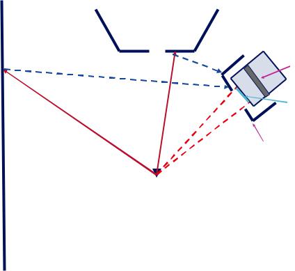
21 or even eliminated. . Figure 21.8 depicts the idealized view of the emission of X-rays generated by the electron beam in the SEM. In this idealized view, the only X-rays that are collected are those emitted into the solid angle of acceptance of the detector, which is defined by a cone whose apex is centered on the specimen interaction volume, whose altitude is the specimen-to-detector distance, and whose base is the active area of the detector that is not shielded by the
Final lens
EDS detector
window
 Specimen x-rays
. Fig. 21.8 Ideal view of the collection angle of an EDS system
21.4 · Pathological Electron Scattering Can Produce “Trace” Contributions to EDS Spectra |
|
|
351 |
|
|
21 |
|||
|
|
|
|
|
|
|
|||
|
|
|
|
|
|
|
|||
. Fig. 21.9 Effect of backscat- |
|
|
|
|
|
|
|
|
|
tering to produce remote X-ray |
|
|
|
|
|
|
|
|
|
sources on SEM components |
|
Final |
|
|
|
|
|
|
|
|
|
|
|
|
|
|
|
||
(objective lens, chamber walls, |
|
|
|
|
|
|
|
|
|
|
lens |
|
|
|
|
|
|
|
|
stage, etc.) and use of collimator |
|
|
|
|
|
|
|
|
|
|
|
|
|
|
|
|
|
|
|
to block these contributions from |
|
|
|
|
|
|
|
|
|
reaching the EDS |
Remote X-rays |
|
|
|
EDS |
|
|||
|
|
|
|
detector |
|
||||
|
|
|
|
|
|
|
|||
|
|
|
|
|
|
window |
|
||
|
|
|
|
BSE |
|
||||
|
|
BSE |
|
|
|
|
|
|
|
|
Chamber |
|
|
|
Collimator & |
|
|||
|
|
|
|
electron trap |
|
||||
|
wall |
|
Specimen X-rays |
|
|||||
|
|
|
|
|
|||||
|
|
|
|
|
|
|
|
|
|
|
|
|
|
|
|
|
|
|
|
|
|
|
|
|
|
|
|
|
|
entrance window or other hardware. However, the reality of the EDS measurement is likely to be quite different from this ideal case, at least at the trace constituent level, as a consequence of electron backscattering, shown schematically in . Fig. 21.9. For targets of intermediate and high atomic number, a significant fraction of the incident beam is emitted as backscattered electrons, and the majority of these BSEs retain more than half of the incident beam energy. After leaving the specimen, these BSEs are likely to strike the objective lens and the walls of the specimen chamber as well as other hardware, where they generate the characteristic (and continuum) X-rays of those materials. The EDS detector collects X-rays from any source with a line-of-sight to the detector, so to minimize remote BSEinduced contributions to the measured spectrum, the EDS is equipped with a collimator whose function is to restrict the view of the EDS, as illustrated schematically in
. Fig. 21.9. The solid angle of acceptance of the EDS is substantially reduced by the collimator, minimizing remote contributions from the lens and chamber walls. While the collimator provides a critical improvement to the measured spectrum, it is important for the analyst to understand its inevitable limitations. The actual acceptance solid angle must be constructed by looking out from the detector
through the |
aperture of the collimator, as shown in |
. Fig. 21.10. |
The typical collimator accepts X-rays |
generated in the specimen plane within a circular area with a diameter of several millimeters, a feature that is important for X-ray mapping applications, where the beam is scanned over large lateral areas and X-rays must be accepted from any beam position within the scanned area. Moreover, the acceptance region is three dimensional with a vertical dimension of several millimeters along the beam axis. To determine the true acceptance volume of the EDS collimator, low magnification (maximum scanning area) X-ray mapping of a target such as a blank aluminum sample stub provides a direct view of the transmission of the EDS collimator as a function of x-y position and as a function of the z-position, as shown in . Fig. 21.11. For this example, any X-ray generated in a large volume (at least 2.5 × 3 × 10 mm) can potentially be collected by this EDS system despite the otherwise effective collimator. Three important sources of uncontrolled remote excitation within this collimator acceptance volume are shown in . Fig. 21.12: (1) beam electrons scattering off the edge of the final aperture (magenta trajectory); (2) beam electrons being stopped by the final aperture and generating the characteristic and continuum X-rays of the aperture material (e.g., Pt; blue dashed trajectory); and (3) re-scattering of BSEs that have struck the final lens and return to the specimen (red trajectory). Both of these sources can create X-rays several millimeters or more from the beam impact location.
352\ Chapter 21 · Trace Analysis by SEM/EDS
. Fig. 21.10 True extent of acceptance area of EDS constructed by looking out through the collimator
|
Final |
|
|
lens |
|
Remote X-rays |
EDS |
|
detector |
||
|
||
|
window |
BSE |
|
BSE |
|
Chamber |
Collimator & |
electron trap |
|
wall |
Specimen X-rays |
|
|
|
Green = |
|
Extent of |
Several mm |
specimen |
|
X-ray sources |
|
NOT excluded |
|
by collimator |
. Fig. 21.11 X-ray mapping to determine the acceptance volume of the collimator. A series of Al X-ray maps of an aluminum SEM stub at different working distances is shown; the inset graph shows the intensity at the center of each map as a function of working distance
counts/pixel |
1200 |
|
|
|
|
|
|
|
|
|
|
|
|
|
|
|
|
|
|
|
|
||
1000 |
|
|
|
|
|
|
|
|
|
|
|
|
|
|
|
|
|
|
|
|
|
|
|
|
800 |
|
|
|
|
|
|
|
|
|
|
|
|
|
|
|
|
|
|
|
|
|
|
|
600 |
|
|
|
|
|
|
|
|
|
|
|
|
|
|
|
|
|
|
|
|
|
|
|
400 |
|
|
|
|
|
|
|
|
|
|
|
|
|
|
|
|
|
|
|
|
|
|
Al |
200 |
|
|
|
|
|
|
|
|
|
|
|
|
|
|
|
|
|
|
|
|
||
|
0 |
|
|
|
|
|
|
|
|
|
|
|
8 |
10 |
12 |
14 |
16 |
18 |
20 |
22 |
|||
|
|
|
|
|
Working distance (mm) |
|
|
|
|||
10 mm |
|
|
|
12 mm |
|
|
|
14 mm |
|
|
|
16 mm |
18 mm |
20 mm |
21
1 mm
Al machined surface  0 10 20 30 40 50 60 70 80 90 100

21.4 · Pathological Electron Scattering Can Produce “Trace” Contributions to EDS Spectra |
|
|
|
|
353 |
|
|
21 |
|||||
|
|
|
|
|
|
|
|
||||||
|
|
|
|
|
|
|
|
||||||
. Fig. 21.12 Possible sources |
|
|
|
|
|
Aperture |
Conventional SEM, |
|
|||||
of remote excitation: beam elec- |
Final lens |
|
|
|
|
|
|||||||
|
|
scattering |
|
||||||||||
trons scattering off edge of final |
|
|
|
|
|
pathological scattering |
|
||||||
|
|
|
|
|
|
|
|
|
|||||
aperture, beams stopped by |
Final aperture |
|
|
|
|
|
|
|
|
||||
aperture generating characteris- |
|
|
|
|
|
|
|
|
|||||
tic and continuum X-rays, and |
|
|
|
|
|
|
|
|
|
EDS |
|
||
|
|
|
|
|
|
|
|
|
|
||||
re-scattering of backscattered |
Remote X-rays |
|
|
|
|
|
|||||||
|
|
|
|
detector |
|
||||||||
electrons from the lens |
|
|
|
|
|
|
|
|
|
|
|||
|
|
|
|
|
|
|
|
|
|
window |
|
||
|
|
|
BSE |
|
BSE |
|
|
|
|
|
|||
|
|
|
|
|
|
|
|
|
|
|
|||
|
Chamber |
|
|
|
|
Collimator & |
|
||||||
|
|
|
|
|
electron trap |
|
|||||||
|
wall |
|
|
|
|
|
|||||||
|
|
|
Specimen X-rays |
|
|||||||||
|
|
|
|
|
|
|
|
|
|||||
|
|
|
|
|
|
|
|
|
|
|
|
|
|
|
Green = |
Several mm |
Extent of |
|
specimen |
|
X-ray sources |
|
NOT excluded |
|
by collimator |
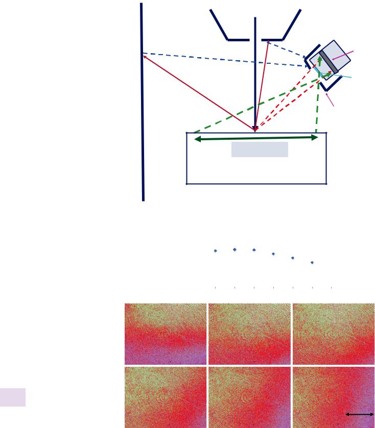
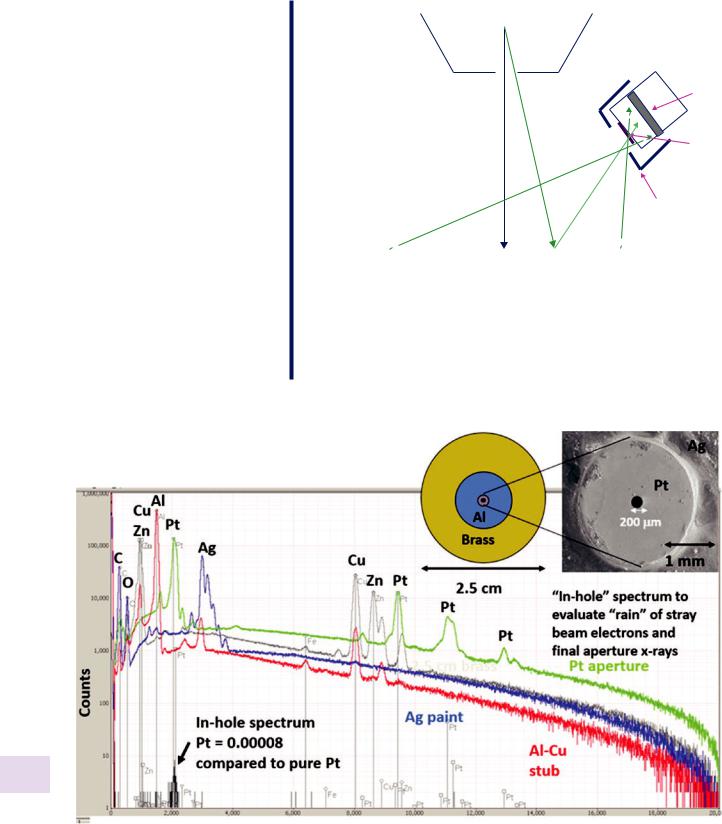
21.4.2\ Assessing Remote Excitation Sources
in an SEM-EDS System
Remote excitation of X-rays can be assessed by measuring various structures. As shown in . Fig. 21.13, a multi-mate- rial Faraday cup can be constructed by placing an SEM aperture (typically 2.5 mm in diameter and made of platinum or another heavy metal) over a blind hole drilled in a block of a different metal, such as a 1-cm diameter aluminum SEM stub, which is then inserted in a hole drilled in a 2.5-cm-diameter brass (Cu-Zn) block. This structure can be used to measure the “in-hole” spectrum to assess sources and magnitude of remote excitation (Williams and Goldstein 1981). The following sequence of measurements is made, as shown in . Fig. 21.14. The beam is successively placed for the same dose on the brass, the Al-stub, the Pt-aperture, and finally in the center of the hole (e.g., 200-μm diameter) of the aperture. Ideally, if there are no electrons scattered outside the beam by interacting with the final aperture or other electron column surfaces, the “in-hole” specimen will have no counts. As shown in . Fig. 21.14 with a logarithmic intensity display, a small number of counts is detected for Pt M, equivalent to k = 0.00008 of the intensity measured for the same dose with the beam placed on the Pt aperture. No detectable counts are found for Al from the stub or for the Cu and Zn from the brass block. Thus, for this particular instrument, a small but detectable pathological scattering occurs within approximately 1.5 mm of the central beam axis. While this is a very small effect, the analyst must nonetheless be aware that this unfocused electron or aperture X-ray source might contribute an artifact at the trace level if
the element of interest at the beam location is abundant in a nearby region.
While a useful measurement and the place to start in assessing remote excitation, the “in-hole” measurement only detects electrons scattered outside of the beam. Typically, a more serious source of remote excitation is the backscattered electrons (BSEs), which are absent from the “in-hole” measurement.
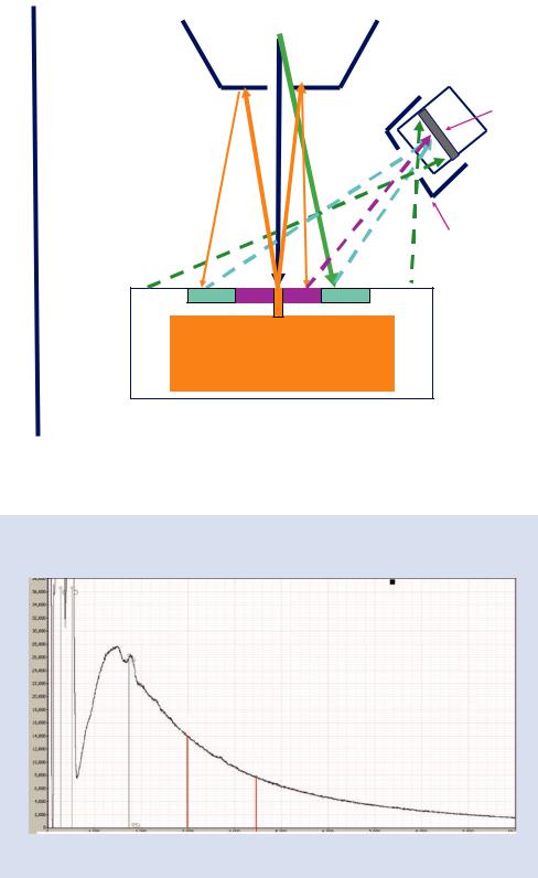
. Figure 21.15 shows a modification of the “in-hole” multimaterial target in which the central hole is replaced by a flat, polished scattering target. . Figure 21.16 shows an example of a spectrum in which the central target is high purity carbon, which has a low BSE coefficient of 0.06, surrounded by a 3-mm- diameter region filled with Ag-epoxy, which is surrounded by a Ti block. No detectable counts for characteristic peaks of Ag (conducting epoxy) or Ti (specimen holder) are found.
. Figure 21.17 shows a similar measurement for high purity tantalum, which has a high BSE coefficient of 0.45. Both Ag and Ti are detectable at very low relative intensity compared to the intensity measured with the beam placed on pure element targets.
When a three-dimensional target is used for scattering, as illustrated in . Fig. 21.18, additional BSEs are scattered from the tilted surfaces into the regions of the specimen near the beam impact point as well as more distant regions surrounding the specimen. . Figure 21.19 shows such a measurement for a pyramidal fragment of SrF2 placed on a brass substrate. Low level signals are observed for CuKα and ZnKα, and also for NiKα, which arises from Ni-plating on nearby stage components. This extreme case most closely resembles the challenge posed by a rough, topographic specimen. The uncontrollable scattering renders most trace constituent determinations questionable.
354\ Chapter 21 · Trace Analysis by SEM/EDS
. Fig. 21.13 Measurement of “in-hole” spectrum with a multi-material Faraday cup consisting of three materials arranged concentrically
|
Aperture |
Conventional SEM, |
|
|
scattering |
||
Final |
pathological scattering |
||
|
|||
|
|
||
lens |
|
|
|
|
|
EDS |
|
|
|
detector |
|
|
|
window |
Chamber |
Collimator & |
||||||||||
electron trap |
|||||||||||
wall |
|||||||||||
|
|||||||||||
|
|
|
|
|
|
|
|
|
|
Green = |
|
|
|
|
|
|
|
|
|
|
|
||
|
|
|
|
|
|
|
|
|
|
||
|
|
|
|
|
|
|
|
|
|
Extent of |
|
|
|
|
|
|
|
|
|
|
|
specimen |
|
|
|
|
|
|
|
|
|
|
|
X-ray sources |
|
|
|
|
|
|
|
|
|
|
|
||
|
|
|
|
|
|
|
|
|
|
NOT excluded |
|
|
|
|
“In-hole Spectrum” |
|
|
||||||
|
|
|
|
|
by collimator |
||||||
|
|
|
|
|
|
|
|
|
|
|
|
|
Multi-material Faraday Cup “in-hole” test specimen |
|
|||||||||
21
0.0 |
2.0 |
4.0 |
6.0 |
8.0 |
10.0 |
12.0 |
14.0 |
16.0 |
18.0 |
20.0 |
Photon energy (keV)
. Fig. 21.14 Sequence of measurements for determining pathological scattering effects by the “in-hole” method. For the same dose, EDS spectra are measured on the brass block, aluminum stub, platinum aperture, and
at the center of the 200 μm diameter hole of the platinum aperture. A logarithmic display reveals the very low counts in the “in-hole” spectrum compared to the spectra measured on the various materials
21.4 · Pathological Electron Scattering Can Produce “Trace” Contributions to EDS Spectra
. Fig. 21.15 Schematic |
|
|
diagram of the “in-hole” |
|
|
configuration with a pure |
Final |
|
element target placed at the |
||
lens |
||
center of a multi-material target |
||
|
BSE
355 |
|
21 |
|
|
|
Aperture |
Conventional SEM, |
|
scattering |
||
pathological scattering |
||
|
EDS detector
 window
Chamber wall
Spectrum from high purity flat scattering target, e.g., C, Ta, surrounded by different materials, e.g., Ag-epoxy, Ti, Al
Collimator & electron trap
Green =
Extent of specimen X-ray sources NOT excluded by collimator
Multi-material “flat scatter” test specimen
. Fig. 21.16 Measurement of high purity C surrounded by Ag (doped epoxy) and titanium; no significant signals for Ag or Ti are observed
C K + C K
C K
Si K-edge
Counts
Ag
FullamplainC_20kV25nAME 112kHz12DT500s10kx_02-09-09
Carbon
E0 = 20 keV
12% deadtime, 112 kHz
500s (12,500 nA-s)
0.1 – 20 keV integral = 56 million counts
Ti
0 |
1.0 |
2.0 |
3.0 |
4.0 |
5.0 |
6.0 |
7.0 |
8.0 |
9.0 |
10.0 |
Photon energy (keV)

356\ Chapter 21 · Trace Analysis by SEM/EDS
. Fig. 21.17 Measurement of high purity Ta surrounded by Ag (doped epoxy) and titanium; Ag or Ti are both observed at very low levels: Ag, k = 0.000003; Ti, k = 0.000005
Counts
Ag = 0.000003 |
|
|
2TaMa,b |
Ti = 0.000005 |
Ta |
Ag |
Ti |
E0 = 20 keV |
8% Deadtime
0.0 |
2.0 |
4.0 |
6.0 |
8.0 |
10.0 |
12.0 |
14.0 |
16.0 |
18.0 |
20 |
Photon energy (keV)
. Fig. 21.18 Modification of the “in-hole” configuration with a three-dimensional target to produce the effects of backscattering from inclined surfaces
Chamber wall
21
Aperture |
Conventional SEM, |
|
scattering |
||
pathological scattering |
||
Final |
||
|
||
lens |
|
EDS
 detector

 window
 Collimator &
electron trap
|
|
|
|
|
|
Green = |
|
Spectrum from strong |
|
||||
|
|
Extent of |
||||
|
topographic scatterer, e.g., SrF2, |
|
||||
|
|
specimen |
||||
|
surrounded by different |
|
||||
|
|
X-ray sources |
||||
|
materials, e.g., Pt, Ti |
|
||||
|
|
NOT excluded by |
||||
|
|
|
|
|
|
|
Multi-material “topographic scatter” test specimen |
collimator |
|||||
|
||||||