


8XC196Kx, Jx, CA USER’S MANUAL
2.2DEVICE FEATURES
Table 2-1 lists the features of each member of the 8XC196Kx family.
Table 2-1. Features of the 8XC196Kx, Jx, CA Product Family
|
|
OTPROM/ |
Register |
Code/ |
I/O |
EPA |
SIO/ |
A/D |
External |
|
Device |
Pins |
EPROM/ |
SSIO |
Interrupt |
||||||
RAM (2) |
Data RAM |
Pins |
Pins |
Channels |
||||||
|
|
ROM (1) |
Ports |
Pins |
||||||
|
|
|
|
|
|
|
||||
8XC196JV (3) |
52 |
48 K |
1536 |
512 |
56 |
6 |
3 |
6 |
1 |
|
8XC196KT |
68 |
32 K |
1024 |
512 |
56 |
10 |
3 |
8 |
2 |
|
|
|
|
|
|
|
|
|
|
|
|
8XC196JT (3) |
52 |
32 K |
1024 |
512 |
41 |
6 |
3 |
6 |
1 |
|
87C196CA (4) |
68 |
32 K |
1024 |
256 |
51 |
6 |
3 |
6 |
2 |
|
8XC196KS (3) |
68 |
24 K |
1024 |
256 |
56 |
10 |
3 |
8 |
2 |
|
8XC196KR |
68 |
16 K |
512 |
256 |
56 |
10 |
3 |
8 |
2 |
|
|
|
|
|
|
|
|
|
|
|
|
8XC196JR |
52 |
16 K |
512 |
256 |
41 |
6 |
3 |
6 |
1 |
|
|
|
|
|
|
|
|
|
|
|
|
8XC196KQ |
68 |
12 K |
384 |
128 |
56 |
10 |
3 |
8 |
2 |
|
|
|
|
|
|
|
|
|
|
|
|
8XC196JQ |
52 |
12 K |
384 |
128 |
41 |
6 |
3 |
6 |
1 |
|
|
|
|
|
|
|
|
|
|
|
NOTES:
1.Optional. The second character of the device name indicates the presence and type of nonvolatile memory. 80C196xx = none; 83C196xx = ROM; 87C196xx = OTPROM or EPROM.
2.Register RAM amounts include the 24 bytes allocated to core SFRs and the stack pointer.
3.The 8XC196JT, JV, and KS are offered in automotive temperature ranges only. The 87C196CA, 8XC196JQ, JR, KQ, KR, and KT are offered in both automotive and commercial temperature ranges.
4.The 87C196CA also has an on-chip networking peripheral that supports CAN specification 2.0.
2.3BLOCK DIAGRAM
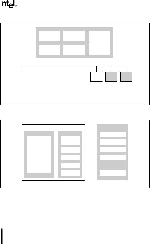
Figure 2-1 shows the major blocks within the device. The core of the device (Figure 2-2) consists of the central processing unit (CPU) and memory controller. The CPU contains the register file and the register arithmetic-logic unit (RALU). The CPU connects to both the memory controller and an interrupt controller via a 16-bit internal bus. An extension of this bus connects the CPU to the internal peripheral modules. In addition, an 8-bit internal bus transfers instruction bytes from the memory controller to the instruction register in the RALU.
2-2
ARCHITECTURAL OVERVIEW
Core |
|
Optional |
|
ROM |
|
|
|
|
|
|
|
|
|
|
Clock and |
|
Code/Data |
Power Mgmt. |
|
RAM |
|
|
|
|
|
|
|
|
|
|
|
|
|
|
|
|
|
|
|
|
|
|
|
|
|
|
|
|
|
|
|
|
|
|
|
|
|
|
|
|
|
|
|
|
|
|
|
I/O |
|
|
SIO |
|
|
SSIO |
|
|
EPA |
|
|
|
A/D |
|
||||
|
|
|
|
|
|
|
|
|
|
|
|
|
|
|
|
|
|
|
|
|
|
|
|
|
|
|
|
|
|
|
|
|
|
|
|
|
|
|
|
|
|
Note:
The slave port is unique to 8XC196Kx devices. The CAN peripheral is unique to the 8XC196CA.
Interrupt
Controller
PTS
Slave
WDT CAN
Port
A2799-02
Figure 2-1. 8XC196Kx Block Diagram
|
|
CPU |
|
|
Memory Controller |
||||||
|
|
|
|
|
|
|
|
|
|
|
|
|
Register File |
|
|
|
|
RALU |
|
|
Prefetch Queue |
|
|
|
|
|
|
|
|
Microcode |
|
|
|
|
|
|
|
|
|
|
|
|
|
|
|
|
|
|
|
|
|
|
|
Engine |
|
|
|
Slave PC |
|
|
Register |
|
|
|
|
|
|
|
|
|
|
|
|
|
|
|
|
|
|
|
|
|
|
|
|
|
|
|
ALU |
|
|
|
Address Register |
|
|
|
RAM |
|
|
|
|
|
|
|
|
||
|
|
|
|
|
|
|
|
|
|
|
|
|
|
|
|
|
|
Master PC |
|
|
|
Data Register |
|
|
|
|
|
|
|
|
|
|
|
|
|
|
|
|
|
|
|
PSW |
|
|
|
|
|
|
CPU SFRs |
|
|
|
|
|
|
|
|
|
|
|
|
|
|
|
Registers |
|
|
|
Bus Controller |
|
|
|
|
|
|
|
|
|
|
|
|
||
|
|
|
|
|
|
|
|
|
|
|
|
|
|
|
|
|
|
|
|
|
|
|
|
|
|
|
|
|
|
|
|
|
|
|
|
A2797-01
Figure 2-2. Block Diagram of the Core
2-3
8XC196Kx, Jx, CA USER’S MANUAL
2.3.1CPU Control
The CPU is controlled by the microcode engine, which instructs the RALU to perform operations using bytes, words, or double words from either the 256-byte lower register file or through a window that directly accesses the upper register file. (See Chapter 4, “Memory Partitions,” for more information about the register file and windowing.) CPU instructions move from the 4-byte queue in the memory controller into the RALU’s instruction register. The microcode engine decodes the instructions and then generates the sequence of events that cause desired functions to occur.
2.3.2Register File
The register file is divided into an upper and a lower file. In the lower register file, the lowest 24 bytes are allocated to the CPU’s special-function registers (SFRs) and the stack pointer, while the remainder is available as general-purpose register RAM. The upper register file contains only general-purpose register RAM. The register RAM can be accessed as bytes, words, or doublewords.
The RALU accesses the upper and lower register files differently. The lower register file is always directly accessible with register-direct addressing (see “Addressing Modes” on page 3-5). The upper register file is accessible with register-direct addressing only when windowing is enabled. Windowing is a technique that maps blocks of the upper register file into a window in the lower register file. See Chapter 4, “Memory Partitions,” for more information about the register file and windowing.
2.3.3Register Arithmetic-logic Unit (RALU)
The RALU contains the microcode engine, the 16-bit arithmetic logic unit (ALU), the master program counter (PC), the program status word (PSW), and several registers. The registers in the RALU are the instruction register, a constants register, a bit-select register, a loop counter, and three temporary registers (the upper-word, lower-word, and second-operand registers).
The PSW contains one bit (PSW.1) that globally enables or disables servicing of all maskable interrupts, one bit (PSW.2) that enables or disables the peripheral transaction server (PTS), and six Boolean flags that reflect the state of your program. Appendix A, “Instruction Set Reference” provides a detailed description of the PSW.
All registers, except the 3-bit bit-select register and the 6-bit loop counter, are either 16 or 17 bits (16 bits plus a sign extension). Some of these registers can reduce the ALU’s workload by performing simple operations.
2-4

ARCHITECTURAL OVERVIEW
The RALU uses the upperand lower-word registers together for the 32-bit instructions and as temporary registers for many instructions. These registers have their own shift logic and are used for operations that require logical shifts, including normalize, multiply, and divide operations. The six-bit loop counter counts repetitive shifts. The second-operand register stores the second operand for two-operand instructions, including the multiplier during multiply operations and the divisor during divide operations. During subtraction operations, the output of this register is complemented before it is moved into the ALU.
The RALU speeds up calculations by storing constants (e.g., 0, 1, and 2) in the constants register so that they are readily available when complementing, incrementing, or decrementing bytes or words. In addition, the constants register generates single-bit masks, based on the bit-select register, for bit-test instructions.
2.3.3.1Code Execution
The RALU performs most calculations for the device, but it does not use an accumulator. Instead it operates directly on the lower register file, which essentially provides 256 accumulators. Because data does not flow through a single accumulator, the device’s code executes faster and more efficiently.
2.3.3.2Instruction Format
MCS 96 microcontrollers combine a large set of general-purpose registers with a three-operand instruction format. This format allows a single instruction to specify two source registers and a separate destination register. For example, the following instruction multiplies two 16-bit variables and stores the 32-bit result in a third variable.
MUL RESULT, FACTOR_1, FACTOR_2 |
;multiply FACTOR_1 and FACTOR_2 |
|
;and store answer in RESULT |
|
;(RESULT)←(FACTOR_1 × FACTOR_2) |
An 80C186 device requires four instructions to accomplish the same operation. The following example shows the equivalent code for an 80C186 device.
MOV |
AX, FACTOR_1 |
;move FACTOR_1 into accumulator (AX) |
|
|
;(AX)←FACTOR1 |
MUL |
FACTOR_2 |
;multiply FACTOR_2 and AX |
|
|
;(DX:AX)←(AX)×(FACTOR_2) |
MOV |
RESULT, AX |
;move lower byte into RESULT |
|
|
;(RESULT)←(AX) |
MOV |
RESULT+2, DX |
;move upper byte into RESULT+2 |
|
|
;(RESULT+2)←(DX) |
2-5