

CHAPTER 7
SERIAL I/O (SIO) PORT
A serial input/output (SIO) port provides a means for the system to communicate with external devices. This device has a serial I/O (SIO) port that shares pins with port 2. This chapter describes the SIO port and explains how to configure it. Chapter 6, “I/O Ports,” explains how to configure the port pins for their special functions. Refer to Appendix B for details about the signals discussed in this chapter.
7.1SERIAL I/O (SIO) PORT FUNCTIONAL OVERVIEW
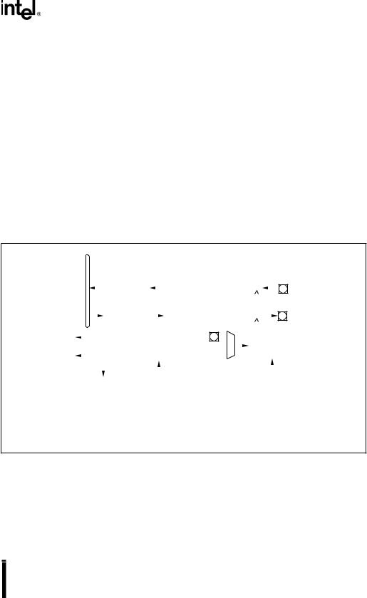
The serial I/O port (Figure 7-1) is an asynchronous/synchronous port that includes a universal asynchronous receiver and transmitter (UART). The UART has one synchronous mode (mode 0) and three asynchronous modes (modes 1, 2, and 3) for both transmission and reception.
Internal
Data
Bus
|
|
|
|
|
|
|
SBUF_RX |
|
|
|
|
|
|
Receive Shift Register |
|
|
|
|
|
|
RXD |
|||||||||||||
|
|
|
|
|
|
|
|
|
|
|
|
|
|
|
|
|
|
|
||||||||||||||||
|
|
|
|
|
|
|
|
|
|
|
|
|
|
|
|
|
|
|
|
|
|
|
|
|
|
|
|
|
|
|
||||
|
|
|
|
|
|
|
|
|
|
|
|
|
|
|
|
|
|
|
|
|
|
|
|
|
|
|
|
|
|
|
|
|
|
|
|
|
|
|
|
|
|
|
|
|
|
|
|
|
|
|
|
|
|
|
|
|
|
|
|
|
|
|
|
|
|
||||
|
|
|
|
|
|
|
SBUF_TX |
|
|
|
|
|
|
Transmit Shift Register |
|
|
|
|
|
|
TXD |
|||||||||||||
|
|
|
|
|
|
|
|
|
|
|
|
|
|
|
|
|
|
|||||||||||||||||
|
|
|
|
|
|
|
|
|
|
|
|
|
|
|
|
|
|
|
|
|
|
|
|
|
|
|
|
|
|
|
|
|
|
|
|
|
|
|
|
|
|
|
|
|
|
|
|
|
|
|
|
|
|
|
|
|
|
|
|
|
|
|
|
|
|
|
|
|
|
TI |
|
|
|
|
|
|
|
|
|
|
|
|
|
|
|
|
T1CLK |
|
|
|
0 |
|
|
|
|
|
|
|
|
|
|
|
|
|
|
|
|
|
|
|
Control Logic |
|
|
|
|
|
|
Baud Rate |
|
||||||||||||||||||||
Interrupts |
|
|
|
|
|
|
|
|
|
|
|
|
|
|
|
|
|
|||||||||||||||||
|
|
|
|
|
|
XTAL1 |
|
|
1 |
|
|
|
|
Generator |
|
|||||||||||||||||||
RI |
|
|
|
|
|
|
|
|
|
|
|
|
|
|
|
|
|
|
|
|
|
|
|
|||||||||||
|
|
|
|
|
|
|
|
|
|
|
|
|
|
|
|
|
|
|
|
|||||||||||||||
|
|
|
|
|
|
|
|
|
|
|
|
|
|
|
|
|
|
|
|
|
|
|
|
|
|
|
|
|
|
|
|
|
|
|
|
|
|
|
|
|
|
|
|
|
|
|
|
|
|
|
|
|
|
|
|
|
|
|
|
|
|
|
|
|
|
|
|
|
|
|
|
|
|
|
|
|
|
|
|
|
|
|
|
|
|
|
|
|
|
|
|
|
|
|
|
|
|
|
|
|
|
|
|
|
|
|
SP_STATUS |
|
|
SP_CON |
|
|
|
|
|
|
|
|
|
|
SP_BAUD |
||||||||||||||||||
|
|
|
|
|
|
|
|
|
|
|
|
|
|
|
|
|
|
|
|
|
|
|
|
|
|
|
||||||||
|
|
|
|
|
|
|
|
|
|
|
|
|
|
|
|
|
|
|
|
|
|
MSB |
|
|
|
|
|
|
|
|
|
|
||
|
|
|
|
|
|
|
|
|
|
|
|
|
|
|
|
|
|
|
|
|
|
|
|
|
|
|
|
|
|
|||||
Note:
The T1CLK clock source is unique to the 8XC196Kx.
For the 8XC196CA and Jx, XTAL1 must provide the clock signal.
A3137-01
Figure 7-1. SIO Block Diagram
The serial port receives data into the receive buffer; it transmits data from the port through the transmit buffer. The transmit and receive buffers are separate registers, permitting simultaneous reads and writes to both. The transmitter and receiver are buffered to support continuous transmissions and to allow reception of a second byte before the first byte has been read.
7-1

8XC196Kx, Jx, CA USER’S MANUAL
An independent, 15-bit baud-rate generator controls the baud rate of the serial port. Either XTAL1 or T1CLK can provide the clock signal. The baud-rate register (SP_BAUD) selects the clock source and the baud rate.
7.2SERIAL I/O PORT SIGNALS AND REGISTERS
Table 7-1 describes the SIO signals and Table 7-2 describes the control and status registers.
Table 7-1. Serial Port Signals
|
|
|
Serial |
|
Port |
|
Serial Port |
Port |
Description |
Pin |
|
Signal |
Signal |
|
|
|
|||
|
|
|
Type |
|
|
|
|
|
|
P2.0 |
|
TXD |
O |
Transmit Serial Data |
|
|
|
|
In modes 1, 2, and 3, TXD transmits serial port output data. In mode 0, |
|
|
|
|
it is the serial clock output. |
|
|
|
|
|
P2.1 |
|
RXD |
I/O |
Receive Serial Data |
|
|
|
|
In modes 1, 2, and 3, RXD receives serial port input data. In mode 0, it |
|
|
|
|
functions as an input or an open-drain output for data. |
|
|
|
|
|
P6.2 |
|
T1CLK † |
I |
Timer 1 Clock |
|
|
|
|
External clock source for the baud-rate generator input. |
|
|
|
|
|
† |
The T1CLK pin is not implemented on the 8XC196CA, JQ, JR, JT, JV devices. XTAL1 must provide |
|||
the serial port clock. |
|
|
||
Table 7-2. Serial Port Control and Status Registers
Mnemonic |
Address |
Description † |
INT_MASK1 |
0013H |
Interrupt Mask 1 |
|
|
Setting the TI bit enables the transmit interrupt; clearing the bit |
|
|
disables (masks) the interrupt. |
|
|
Setting the RI bit enables the receive interrupt; clearing the bit |
|
|
disables (masks) the interrupt. |
|
|
|
INT_PEND1 |
0012H |
Interrupt Pending 1 |
|
|
When set, the TI bit indicates a pending transmit interrupt. |
|
|
When set, the RI bit indicates a pending receive interrupt. |
|
|
|
†Except as otherwise noted, write zeros to the reserved bits in these registers.
††The T1CLK pin is not implemented on the 8XC196CA, JQ, JR, JT, JV devices. XTAL1 must provide the serial port clock.
7-2

SERIAL I/O (SIO) PORT
Table 7-2. Serial Port Control and Status Registers (Continued)
Mnemonic |
Address |
Description † |
P2_DIR |
1FCBH |
Port 2 Direction |
|
|
This register selects the direction of each port 2 pin. Clear P2_DIR.1 |
|
|
to configure RXD (P2.1) as a high-impedance input/open-drain |
|
|
output, and set P2_DIR.0 to configure TXD (P2.0) as a comple- |
|
|
mentary output. |
|
|
|
P6_DIR |
1FD2H |
Port 6 Direction |
|
|
This register selects the direction of each port 6 pin. To use T1CLK†† |
|
|
as the input clock to the baud-rate generator, clear P6_DIR.2. |
|
|
|
P2_MODE |
1FC9H |
Port 2 Mode |
|
|
This register selects either the general-purpose input/output function |
|
|
or the peripheral function for each pin of port 2. Set P2_MODE.1:0 |
|
|
to configure TXD (P2.0) and RXD (P2.1) for the SIO port. |
|
|
|
P6_MODE |
1FD1H |
Port 6 Mode |
|
|
This register selects either the general-purpose input/output function |
|
|
or the peripheral function for each pin of port 6. Set P6_MODE.2 to |
|
|
configure T1CLK†† for the SIO port. |
P2_PIN |
1FCFH |
Port 2 Pin State |
|
|
Two bits of this register contain the values of the TXD (P2.0) and |
|
|
RXD (P2.1) pins. Read P2_PIN to determine the current value of the |
|
|
pins. |
|
|
|
P6_PIN |
1FD7H |
Port 6 Pin State |
|
|
If you are using T1CLK (P6.2) as the clock source for the baud-rate |
|
|
generator, you can read P6_PIN.2 to determine the current value of |
|
|
T1CLK†† . |
P2_REG |
1FCDH |
Port 2 Output Data |
|
|
This register holds data to be driven out on the pins of port 2. Set |
|
|
P2_REG.1 for the RXD (P2.1) pin. Write the desired output data for |
|
|
the TXD (P2.0) pin to P2_REG.0. |
|
|
|
P6_REG |
1FD5H |
Port 6 Output Data |
|
|
This register holds data to be driven out on the pins of port 6. To use |
|
|
T1CLK as the clock source for the baud-rate generator, set |
|
|
P6_REG.2. |
|
|
|
SBUF_RX |
1FB8H |
Serial Port Receive Buffer |
|
|
This register contains data received from the serial port. |
|
|
|
SBUF_TX |
1FBAH |
Serial Port Transmit Buffer |
|
|
This register contains data that is ready for transmission. In modes |
|
|
1, 2, and 3, writing to SBUF_TX starts a transmission. In mode 0, |
|
|
writing to SBUF_TX starts a transmission only if the receiver is |
|
|
disabled (SP_CON.3=0) |
|
|
|
†Except as otherwise noted, write zeros to the reserved bits in these registers.
††The T1CLK pin is not implemented on the 8XC196CA, JQ, JR, JT, JV devices. XTAL1 must provide the serial port clock.
7-3