- •Features
- •Pin Configurations
- •Disclaimer
- •Overview
- •Block Diagram
- •AT90S8535 Compatibility
- •Pin Descriptions
- •Port A (PA7..PA0)
- •Port B (PB7..PB0)
- •Port C (PC7..PC0)
- •Port D (PD7..PD0)
- •RESET
- •XTAL1
- •XTAL2
- •AVCC
- •AREF
- •Resources
- •AVR CPU Core
- •Introduction
- •Architectural Overview
- •Status Register
- •Stack Pointer
- •Interrupt Response Time
- •SRAM Data Memory
- •Data Memory Access Times
- •EEPROM Data Memory
- •EEPROM Read/Write Access
- •I/O Memory
- •Clock Systems and their Distribution
- •Clock Sources
- •Default Clock Source
- •Crystal Oscillator
- •External RC Oscillator
- •External Clock
- •Timer/Counter Oscillator
- •Idle Mode
- •Power-down Mode
- •Power-save Mode
- •Standby Mode
- •Extended Standby Mode
- •Analog-to-Digital Converter
- •Analog Comparator
- •Brown-out Detector
- •Internal Voltage Reference
- •Watchdog Timer
- •Port Pins
- •Resetting the AVR
- •Reset Sources
- •Power-on Reset
- •External Reset
- •Brown-out Detection
- •Watchdog Reset
- •Watchdog Timer
- •Timed Sequences for Changing the Configuration of the Watchdog Timer
- •Safety Level 0
- •Safety Level 1
- •Safety Level 2
- •Interrupts
- •I/O-Ports
- •Introduction
- •Configuring the Pin
- •Reading the Pin Value
- •Unconnected pins
- •Alternate Port Functions
- •Alternate Functions of Port A
- •Alternate Functions Of Port B
- •Alternate Functions of Port C
- •Alternate Functions of Port D
- •External Interrupts
- •8-bit Timer/Counter0 with PWM
- •Overview
- •Registers
- •Definitions
- •Counter Unit
- •Output Compare Unit
- •Force Output Compare
- •Modes of Operation
- •Normal Mode
- •Fast PWM Mode
- •Phase Correct PWM Mode
- •Internal Clock Source
- •Prescaler Reset
- •External Clock Source
- •16-bit Timer/Counter1
- •Overview
- •Registers
- •Definitions
- •Compatibility
- •Counter Unit
- •Input Capture Unit
- •Input Capture Trigger Source
- •Noise Canceler
- •Using the Input Capture Unit
- •Output Compare Units
- •Force Output Compare
- •Modes of Operation
- •Normal Mode
- •Fast PWM Mode
- •Phase Correct PWM Mode
- •8-bit Timer/Counter2 with PWM and Asynchronous Operation
- •Overview
- •Registers
- •Definitions
- •Counter Unit
- •Output Compare Unit
- •Force Output Compare
- •Modes of Operation
- •Normal Mode
- •Fast PWM Mode
- •Phase Correct PWM Mode
- •Timer/Counter Prescaler
- •Slave Mode
- •Master Mode
- •Data Modes
- •USART
- •Overview
- •Clock Generation
- •External Clock
- •Synchronous Clock Operation
- •Frame Formats
- •Parity Bit Calculation
- •USART Initialization
- •Sending Frames with 5 to 8 Data Bits
- •Sending Frames with 9 Data Bits
- •Parity Generator
- •Disabling the Transmitter
- •Receiving Frames with 5 to 8 Data Bits
- •Receiving Frames with 9 Data Bits
- •Receiver Error Flags
- •Parity Checker
- •Disabling the Receiver
- •Flushing the Receive Buffer
- •Asynchronous Data Recovery
- •Using MPCM
- •Write Access
- •Read Access
- •Two-wire Serial Interface
- •Features
- •TWI Terminology
- •Electrical Interconnection
- •Transferring Bits
- •START and STOP Conditions
- •Address Packet Format
- •Data Packet Format
- •Overview of the TWI Module
- •SCL and SDA Pins
- •Bit Rate Generator Unit
- •Bus Interface Unit
- •Address Match Unit
- •Control Unit
- •TWI Register Description
- •Using the TWI
- •Transmission Modes
- •Master Transmitter Mode
- •Master Receiver Mode
- •Slave Receiver Mode
- •Slave Transmitter Mode
- •Miscellaneous States
- •Analog Comparator
- •Analog Comparator Multiplexed Input
- •Features
- •Operation
- •Starting a Conversion
- •Differential Gain Channels
- •Changing Channel or Reference Selection
- •ADC Input Channels
- •ADC Voltage Reference
- •ADC Noise Canceler
- •Analog Input Circuitry
- •ADC Accuracy Definitions
- •ADC Conversion Result
- •ADLAR = 0
- •ADLAR = 1
- •Boot Loader Features
- •Application Section
- •Boot Loader Lock Bits
- •Performing a Page Write
- •Using the SPM Interrupt
- •Setting the Boot Loader Lock Bits by SPM
- •Reading the Fuse and Lock Bits from Software
- •Preventing Flash Corruption
- •Simple Assembly Code Example for a Boot Loader
- •Fuse Bits
- •Latching of Fuses
- •Signature Bytes
- •Calibration Byte
- •Signal Names
- •Parallel Programming
- •Enter Programming Mode
- •Chip Erase
- •Programming the Flash
- •Programming the EEPROM
- •Reading the Flash
- •Reading the EEPROM
- •Programming the Lock Bits
- •Reading the Signature Bytes
- •Reading the Calibration Byte
- •Serial Downloading
- •Data Polling Flash
- •Data Polling EEPROM
- •Electrical Characteristics
- •Absolute Maximum Ratings*
- •DC Characteristics
- •External Clock Drive Waveforms
- •External Clock Drive
- •Two-wire Serial Interface Characteristics
- •ADC Characteristics
- •Active Supply Current
- •Idle Supply Current
- •Standby Supply Current
- •Pin Pullup
- •Pin Driver Strength
- •Internal Oscillator Speed
- •Register Summary
- •Instruction Set Summary
- •Ordering Information
- •Packaging Information
- •Errata
- •Changes from Rev. 2502E-12/03 to Rev. 2502G-06/04
- •Changes from Rev. 2502E-12/03 to Rev. 2502F-06/04
- •Changes from Rev. 2502D-09/03 to Rev. 2502E-12/03
- •Changes from Rev. 2502C-04/03 to Rev. 2502D-09/03
- •Changes from Rev. 2502B-09/02 to Rev. 2502C-04/03
- •Changes from Rev. 2502A-06/02 to Rev. 2502B-09/02
- •Table of Contents
ATmega8535(L)
SRAM Data Memory
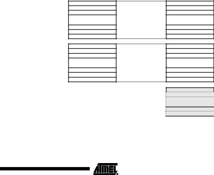
Figure 9 shows how the ATmega8535 SRAM Memory is organized.
The 608 Data Memory locations address the Register File, the I/O Memory, and the internal data SRAM. The first 96 locations address the Register File and I/O Memory, and the next 512 locations address the internal data SRAM.
The five different addressing modes for the data memory cover: Direct, Indirect with Displacement, Indirect, Indirect with Pre-decrement, and Indirect with Post-increment. In the Register File, registers R26 to R31 feature the indirect addressing pointer registers.
The direct addressing reaches the entire data space.
The Indirect with Displacement mode reaches 63 address locations from the base address given by the Y- or Z-register.
When using register indirect addressing modes with automatic pre-decrement and postincrement, the address registers X, Y, and Z are decremented or incremented.
The 32 general purpose working registers, 64 I/O Registers, and the 512 bytes of internal data SRAM in the ATmega8535 are all accessible through all these addressing modes. The Register File is described in “General Purpose Register File” on page 11.
Figure 9. Data Memory Map
Register File
R0
R1
R2
...
R29
R30
R31
I/O Registers
$00
$01
$02
...
$3D
$3E
$3F
Data Address Space
$0000
$0001
$0002
...
$001D
$001E
$001F
$0020
$0021
$0022
...
$005D
$005E
$005F
Internal SRAM
$0060
$0061
...
$025E
$025F
17
2502K–AVR–10/06