

Output Compare Units
measuring frequency only, the clearing of the ICF1 Flag is not required (if an interrupt handler is used).
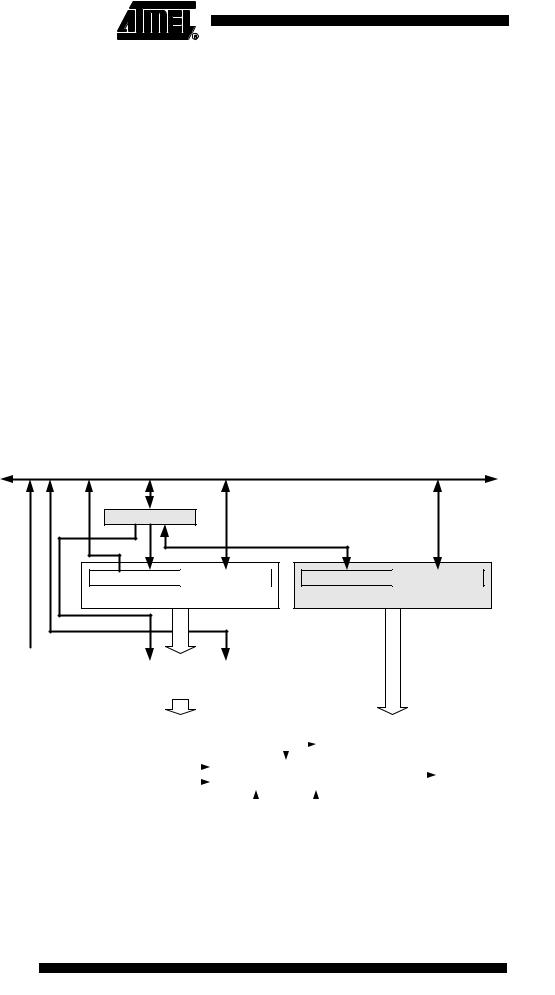
The 16-bit comparator continuously compares TCNT1 with the Output Compare Register (OCR1x). If TCNT equals OCR1x the comparator signals a match. A match will set the Output Compare Flag (OCF1x) at the next timer clock cycle. If enabled (OCIE1x = 1), the Output Compare Flag generates an output compare interrupt. The OCF1x Flag is automatically cleared when the interrupt is executed. Alternatively the OCF1x Flag can be cleared by software by writing a logical one to its I/O bit location. The Waveform Generator uses the match signal to generate an output according to operating mode set by the Waveform Generation mode (WGM13:0) bits and Compare Output mode
(COM1x1:0) bits. The TOP and BOTTOM signals are used by the Waveform Generator for handling the special cases of the extreme values in some modes of operation. (See “Modes of Operation” on page 101.)
A special feature of output compare unit A allows it to define the Timer/Counter TOP value (i.e., counter resolution). In addition to the counter resolution, the TOP value defines the period time for waveforms generated by the Waveform Generator.
Figure 43 shows a block diagram of the output compare unit. The small “n” in the register and bit names indicates the device number (n = 1 for Timer/Counter1), and the “x” indicates output compare unit (A/B). The elements of the block diagram that are not directly a part of the output compare unit are gray shaded.
Figure 43. Output Compare Unit, Block Diagram |
|
|
|
|
DATA BUS (8-bit) |
|
|
TEMP (8-bit) |
|
|
|
OCRnxH Buf. (8-bit) |
OCRnxL Buf. (8-bit) |
TCNTnH (8-bit) |
TCNTnL (8-bit) |
OCRnx Buffer (16-bit Register) |
TCNTn (16-bit Counter) |
||
|
|
|
|
|
|
|
|
|
|
|
|
|
|
|
|
|
|
|
|
|
|
|
|
|
|
|
|
|
|
|
|
|
|
|
|
|
|
|
|
|
OCRnxH (8-bit) |
|
OCRnxL (8-bit) |
|
|
|
|
|
|
|
|
|
||||
|
|
|
|
|
|
|
|
|
|
|
|
|
|
|
|
|
||
|
|
|
|
OCRnx (16-bit Register) |
|
|
|
|
|
|
|
|
||||||
|
|
|
|
|
|
|
|
|
|
|
|
|
|
|
|
|
|
|
|
|
|
|
|
|
|
|
|
|
|
|
|
|
|
|
|
|
|
|
|
|
|
|
|
|
|
= (16-bit Comparator ) |
|
|
|
|||||||
|
|
|
|
|
|
|
|
|
|
|
|
|
|
OCFnx (Int.Req.) |
|
|
|
|
|
|
|
|
|
|
|
|
|
|
|
|
|
|
|
|
|||
|
|
|
|
|
|
|
|
|
|
|
|
|
|
|
|
|
|
|
|
|
|
|
TOP |
|
|
|
Waveform Generator |
|
|
|
OCnx |
||||||
|
|
|
|
|
|
|
||||||||||||
|
|
|
BOTTOM |
|
|
|
|
|
|
|||||||||
|
|
|
|
|
|
|
|
|||||||||||
|
|
|
|
|
|
|
|
|
|
|
|
|
|
|
|
|
||
|
|
|
|
|
|
|
|
|
|
|
|
|
|
|
|
|||
|
|
|
|
|
|
|
|
|
|
|
|
|
|
|
|
|
|
|
|
|
|
|
|
|
|
|
|
|
|
|
|
|
|
|
|
|
|
|
|
|
|
|
|
|
|
|
|
|
|
|
|
|
|
|
|
|
|
|
|
|
|
|
|
|
WGMn3:0 |
COMnx1:0 |
|
|
|
||||||
The OCR1x Register is double buffered when using any of the twelve Pulse Width Modulation (PWM) modes. For the Normal and Clear Timer on Compare (CTC) modes of operation, the double buffering is disabled. The double buffering synchronizes the update of the OCR1x Compare Register to either TOP or BOTTOM of the counting
98 ATmega8535(L)
2502K–AVR–10/06

 ATmega8535(L)
sequence. The synchronization prevents the occurrence of odd-length, non-symmetrical
|
PWM pulses, thereby making the output glitch-free. |
|
The OCR1x Register access may seem complex, but this is not the case. When the |
|
double buffering is enabled, the CPU has access to the OCR1x Buffer Register, and if |
|
double buffering is disabled the CPU will access the OCR1x directly. The content of the |
|
OCR1x (Buffer or Compare) Register is only changed by a write operation (the |
|
Timer/Counter does not update this register automatically as does the TCNT1– and |
|
ICR1 Register). Therefore OCR1x is not read via the high byte temporary register |
|
(TEMP). However, it is a good practice to read the low byte first as with accessing other |
|
16-bit registers. Writing the OCR1x Registers must be done via the TEMP Register |
|
since the compare of all 16 bits is done continuously. The high byte (OCR1xH) has to be |
|
written first. When the high byte I/O location is written by the CPU, the TEMP Register |
|
will be updated by the value written. Then when the low byte (OCR1xL) is written to the |
|
lower eight bits, the high byte will be copied into the upper 8-bits of either the OCR1x |
|
Buffer or OCR1x Compare Register in the same system clock cycle. |
|
For more information of how to access the 16-bit registers refer to “Accessing 16-bit |
|
Registers” on page 92. |
Force Output Compare |
In non-PWM waveform generation modes, the match output of the comparator can be |
|
forced by writing a one to the Force Output Compare (FOC1x) bit. Forcing Compare |
|
Match will not set the OCF1x Flag or reload/clear the timer, but the OC1x pin will be |
|
updated as if a real Compare Match had occurred (the COM11:0 bits settings define |
|
whether the OC1x pin is set, cleared or toggled). |
Compare Match Blocking by |
All CPU writes to the TCNT1 Register will block any Compare Match that occurs in the |
TCNT1 Write |
next timer clock cycle, even when the timer is stopped. This feature allows OCR1x to be |
|
initialized to the same value as TCNT1 without triggering an interrupt when the |
|
Timer/Counter clock is enabled. |
Using the Output Compare |
Since writing TCNT1 in any mode of operation will block all compare matches for one |
Unit |
timer clock cycle, there are risks involved when changing TCNT1 when using any of the |
|
output compare channels, independent of whether the Timer/Counter is running or not. |
|
If the value written to TCNT1 equals the OCR1x value, the Compare Match will be |
|
missed, resulting in incorrect waveform generation. Do not write the TCNT1 equal to |
|
TOP in PWM modes with variable TOP values. The Compare Match for the TOP will be |
|
ignored and the counter will continue to 0xFFFF. Similarly, do not write the TCNT1 value |
|
equal to BOTTOM when the counter is down-counting. |
|
The setup of the OC1x should be performed before setting the Data Direction Register |
|
for the port pin to output. The easiest way of setting the OC1x value is to use the Force |
|
Output Compare (FOC1x) strobe bits in Normal mode. The OC1x Register keeps its |
|
value even when changing between Waveform Generation modes. |
|
Be aware that the COM1x1:0 bits are not double buffered together with the compare |
|
value. Changing the COM1x1:0 bits will take effect immediately. |
99
2502K–AVR–10/06
Compare Match Output
Unit
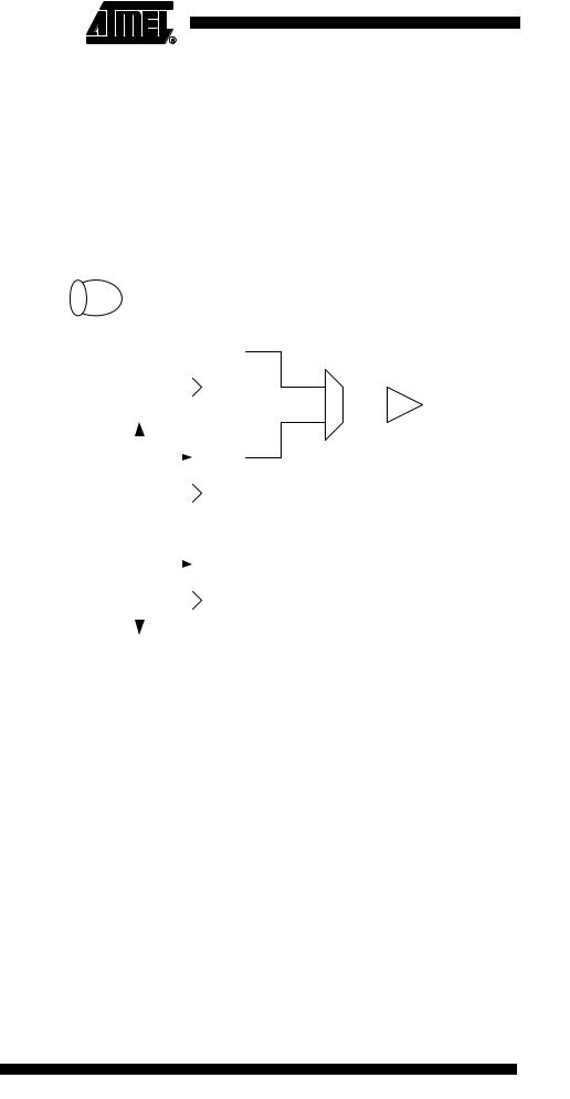
The Compare Output Mode (COM1x1:0) bits have two functions. The waveform generator uses the COM1x1:0 bits for defining the Output Compare (OC1x) state at the next Compare Match. Secondly the COM1x1:0 bits control the OC1x pin output source. Figure 44 shows a simplified schematic of the logic affected by the COM1x1:0 bit setting. The I/O Registers, I/O bits, and I/O pins in the figure are shown in bold. Only the parts of the general I/O port Control Registers (DDR and PORT) that are affected by the COM1x1:0 bits are shown. When referring to the OC1x state, the reference is for the internal OC1x Register, not the OC1x pin. If a System Reset occurs, the OC1x Register is reset to “0”.
Figure 44. Compare Match Output Unit, Schematic
COMnx1 |
|
|
|
|
|
|
|
|
|
|
|
|
|
|
|
|
|
|
|
|
|
|
|
|
|
|
|
|
|
|
|
|
|
|
|
|
|
|
|
|
|
||
|
|
|
|
|
|
|
|
|
|
|
|
|
|
|
|
|
|
|
|
||
|
|
|
|
|
|
|
|
|
|
|
|
|
|
|
|
|
|
|
|
||
|
|
|
|
|
|
|
|
|
|
|
|
|
|
|
|
|
|
|
|
||
|
Waveform |
|
|
|
|
|
|
|
|
|
|
|
|
||||||||
|
|
|
|
|
|
|
|
|
|
|
|
|
|
|
|
|
|||||
COMnx0 |
|
|
|
|
D |
Q |
|
|
|
|
|
|
|
||||||||
|
|
|
|
|
Generator |
|
|
|
|
|
|
|
|
|
|
||||||
FOCnx |
|
|
|
|
|
|
|
|
|
|
|
||||||||||
|
|
|
|
|
|
|
|
|
|
|
|
|
|||||||||
|
|
|
|
|
|
|
|
|
|
|
|
|
|
|
|
|
|
|
|
|
|
|
|
|
|
|
|
|
|
|
|
|
|
|
|
|
1 |
|
|
|
|
|
|
|
|
|
|
|
|
|
|
|
|
|
|
|
|
|
|
|
|
|
OCnx |
||
|
|
|
|
|
|
|
|
|
|
|
|
|
|
|
|
|
|
|
|
|
|
|
|
|
|
|
|
|
|
|
|
|
|
|
OCnx |
0 |
|
|
|
|
Pin |
||
|
|
|
|
|
|
|
|
|
|
|
|
|
|
|
|
|
|||||
|
|
|
|
|
|
|
|
|
|
|
|
|
|
|
|
|
|
|
|
||
|
|
|
|
|
|
|
|
|
|
|
|
|
|
|
|
|
|
|
|
|
|
|
|
|
|
|
|
|
|
BUS |
|
|
|
|
D |
Q |
|
|
|
|
|
|
|
|
|
|
|
|
|
|
|
|
|
|
|
|
|
|
|
|
|
|
|||
|
|
|
|
|
|
|
|
|
|
|
|
|
|
|
|
|
|
|
|||
|
|
|
|
|
|
|
|
|
|
|
|
|
|
|
|
|
|
|
|
||
|
|
|
|
PORT |
|
|
|
|
|
|
|
||||||||||
|
|
|
|
|
|
|
|
DATA |
|
|
|
|
|
|
|
|
|
|
|
|
|
|
|
|
|
D |
Q |
|
|
|
|
|
|
|
|||||||||
|
|
|
|
|
|
|
|
|
|
|
|
|
|
|
|
|
|
|
|
||
|
|
|
|
|
|
|
|
|
|
|
|
|
|
|
|
|
|
|
|
|
|
|
|
|
|
|
|
|
|
|
|
|
|
|
|
|
|
|
|
|
|
|
|
|
clkI/O |
|
|
|
|
|
|
|
|
|
DDR |
|
|
|
|
|
|
|
|||
|
|
|
|
|
|
|
|
|
|
|
|
|
|
|
|
|
|
|
|||
The general I/O port function is overridden by the Output Compare (OC1x) from the waveform generator if either of the COM1x1:0 bits are set. However, the OC1x pin direction (input or output) is still controlled by the Data Direction Register (DDR) for the port pin. The Data Direction Register bit for the OC1x pin (DDR_OC1x) must be set as output before the OC1x value is visible on the pin. The port override function is generally independent of the Waveform Generation mode, but there are some exceptions. Refer to Table 45, Table 46 and Table 47 for details.
The design of the output compare pin logic allows initialization of the OC1x state before the output is enabled. Note that some COM1x1:0 bit settings are reserved for certain modes of operation. See “16-bit Timer/Counter Register Description” on page 110.
The COM1x1:0 bits have no effect on the Input Capture unit.
Compare Output Mode and The Waveform Generator uses the COM1x1:0 bits differently in Normal, CTC, and PWM Waveform Generation modes. For all modes, setting the COM1x1:0 = 0 tells the Waveform Generator that no action on the OC1x Register is to be performed on the next Compare Match. For compare output actions in the non-PWM modes refer to Table 45 on page 110. For fast PWM mode refer to Table 46 on page 111, and for phase correct and phase and fre-
quency correct PWM refer to Table 47 on page 111.
100 ATmega8535(L)
2502K–AVR–10/06