

- •Features
- •Pin Configurations
- •Disclaimer
- •Overview
- •Block Diagram
- •AT90S8535 Compatibility
- •Pin Descriptions
- •Port A (PA7..PA0)
- •Port B (PB7..PB0)
- •Port C (PC7..PC0)
- •Port D (PD7..PD0)
- •RESET
- •XTAL1
- •XTAL2
- •AVCC
- •AREF
- •Resources
- •AVR CPU Core
- •Introduction
- •Architectural Overview
- •Status Register
- •Stack Pointer
- •Interrupt Response Time
- •SRAM Data Memory
- •Data Memory Access Times
- •EEPROM Data Memory
- •EEPROM Read/Write Access
- •I/O Memory
- •Clock Systems and their Distribution
- •Clock Sources
- •Default Clock Source
- •Crystal Oscillator
- •External RC Oscillator
- •External Clock
- •Timer/Counter Oscillator
- •Idle Mode
- •Power-down Mode
- •Power-save Mode
- •Standby Mode
- •Extended Standby Mode
- •Analog-to-Digital Converter
- •Analog Comparator
- •Brown-out Detector
- •Internal Voltage Reference
- •Watchdog Timer
- •Port Pins
- •Resetting the AVR
- •Reset Sources
- •Power-on Reset
- •External Reset
- •Brown-out Detection
- •Watchdog Reset
- •Watchdog Timer
- •Timed Sequences for Changing the Configuration of the Watchdog Timer
- •Safety Level 0
- •Safety Level 1
- •Safety Level 2
- •Interrupts
- •I/O-Ports
- •Introduction
- •Configuring the Pin
- •Reading the Pin Value
- •Unconnected pins
- •Alternate Port Functions
- •Alternate Functions of Port A
- •Alternate Functions Of Port B
- •Alternate Functions of Port C
- •Alternate Functions of Port D
- •External Interrupts
- •8-bit Timer/Counter0 with PWM
- •Overview
- •Registers
- •Definitions
- •Counter Unit
- •Output Compare Unit
- •Force Output Compare
- •Modes of Operation
- •Normal Mode
- •Fast PWM Mode
- •Phase Correct PWM Mode
- •Internal Clock Source
- •Prescaler Reset
- •External Clock Source
- •16-bit Timer/Counter1
- •Overview
- •Registers
- •Definitions
- •Compatibility
- •Counter Unit
- •Input Capture Unit
- •Input Capture Trigger Source
- •Noise Canceler
- •Using the Input Capture Unit
- •Output Compare Units
- •Force Output Compare
- •Modes of Operation
- •Normal Mode
- •Fast PWM Mode
- •Phase Correct PWM Mode
- •8-bit Timer/Counter2 with PWM and Asynchronous Operation
- •Overview
- •Registers
- •Definitions
- •Counter Unit
- •Output Compare Unit
- •Force Output Compare
- •Modes of Operation
- •Normal Mode
- •Fast PWM Mode
- •Phase Correct PWM Mode
- •Timer/Counter Prescaler
- •Slave Mode
- •Master Mode
- •Data Modes
- •USART
- •Overview
- •Clock Generation
- •External Clock
- •Synchronous Clock Operation
- •Frame Formats
- •Parity Bit Calculation
- •USART Initialization
- •Sending Frames with 5 to 8 Data Bits
- •Sending Frames with 9 Data Bits
- •Parity Generator
- •Disabling the Transmitter
- •Receiving Frames with 5 to 8 Data Bits
- •Receiving Frames with 9 Data Bits
- •Receiver Error Flags
- •Parity Checker
- •Disabling the Receiver
- •Flushing the Receive Buffer
- •Asynchronous Data Recovery
- •Using MPCM
- •Write Access
- •Read Access
- •Two-wire Serial Interface
- •Features
- •TWI Terminology
- •Electrical Interconnection
- •Transferring Bits
- •START and STOP Conditions
- •Address Packet Format
- •Data Packet Format
- •Overview of the TWI Module
- •SCL and SDA Pins
- •Bit Rate Generator Unit
- •Bus Interface Unit
- •Address Match Unit
- •Control Unit
- •TWI Register Description
- •Using the TWI
- •Transmission Modes
- •Master Transmitter Mode
- •Master Receiver Mode
- •Slave Receiver Mode
- •Slave Transmitter Mode
- •Miscellaneous States
- •Analog Comparator
- •Analog Comparator Multiplexed Input
- •Features
- •Operation
- •Starting a Conversion
- •Differential Gain Channels
- •Changing Channel or Reference Selection
- •ADC Input Channels
- •ADC Voltage Reference
- •ADC Noise Canceler
- •Analog Input Circuitry
- •ADC Accuracy Definitions
- •ADC Conversion Result
- •ADLAR = 0
- •ADLAR = 1
- •Boot Loader Features
- •Application Section
- •Boot Loader Lock Bits
- •Performing a Page Write
- •Using the SPM Interrupt
- •Setting the Boot Loader Lock Bits by SPM
- •Reading the Fuse and Lock Bits from Software
- •Preventing Flash Corruption
- •Simple Assembly Code Example for a Boot Loader
- •Fuse Bits
- •Latching of Fuses
- •Signature Bytes
- •Calibration Byte
- •Signal Names
- •Parallel Programming
- •Enter Programming Mode
- •Chip Erase
- •Programming the Flash
- •Programming the EEPROM
- •Reading the Flash
- •Reading the EEPROM
- •Programming the Lock Bits
- •Reading the Signature Bytes
- •Reading the Calibration Byte
- •Serial Downloading
- •Data Polling Flash
- •Data Polling EEPROM
- •Electrical Characteristics
- •Absolute Maximum Ratings*
- •DC Characteristics
- •External Clock Drive Waveforms
- •External Clock Drive
- •Two-wire Serial Interface Characteristics
- •ADC Characteristics
- •Active Supply Current
- •Idle Supply Current
- •Standby Supply Current
- •Pin Pullup
- •Pin Driver Strength
- •Internal Oscillator Speed
- •Register Summary
- •Instruction Set Summary
- •Ordering Information
- •Packaging Information
- •Errata
- •Changes from Rev. 2502E-12/03 to Rev. 2502G-06/04
- •Changes from Rev. 2502E-12/03 to Rev. 2502F-06/04
- •Changes from Rev. 2502D-09/03 to Rev. 2502E-12/03
- •Changes from Rev. 2502C-04/03 to Rev. 2502D-09/03
- •Changes from Rev. 2502B-09/02 to Rev. 2502C-04/03
- •Changes from Rev. 2502A-06/02 to Rev. 2502B-09/02
- •Table of Contents
|
|
|
|
|
|
|
|
|
|
|
|
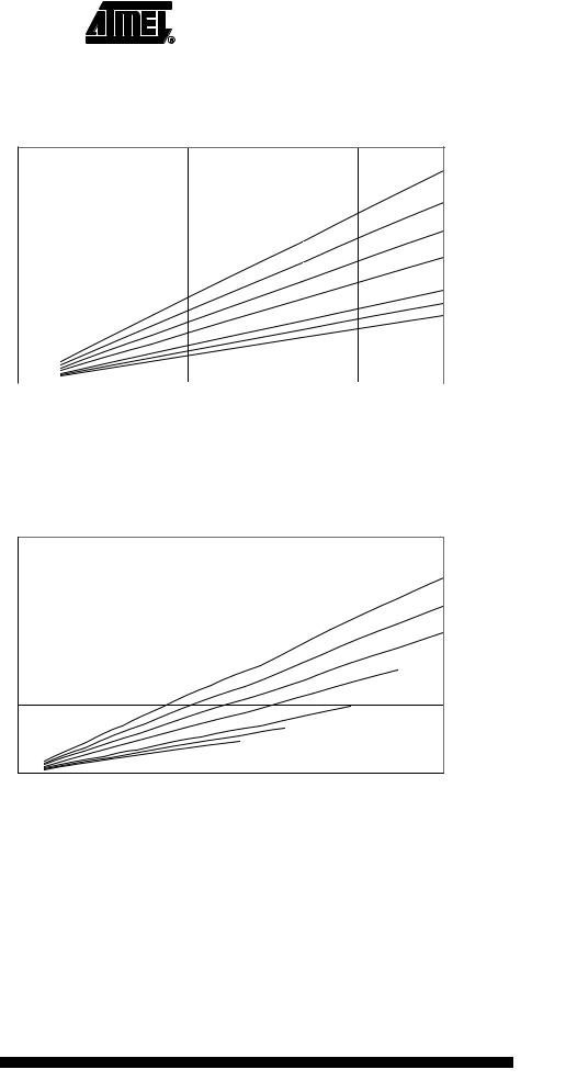
Idle Supply Current |
Figure 137. Idle Supply Current vs. Frequency (0.1 - 1.0 MHz) |
||||
ICC (mA)
IDLE SUPPLY CURRENT vs. FREQUENCY
0.1 - 1.0 MHz
0.8
5.5V
0.7
0.6 |
|
|
|
|
|
|
|
|
|
|
|
|
|
5.0V |
|
|
|
|
|
|
|
|
|
|
|
|
|
4.5V |
|
0.5 |
|
|
|
|
|
|
|
|
|
|
|
|
|
|
|
|
|
|
|
|
|
|
|
|
|
|
|
4.0V |
|
0.4 |
|
|
|
|
|
|
|
|
|
|
|
|
|
|
|
|
|
|
|
|
|
|
|
|
|
|
|
3.3V |
|
0.3 |
|
|
|
|
|
|
|
|
|
|
|
|
|
|
|
|
|
|
|
|
|
|
|
|
|
|
|
3.0V |
|
|
|
|
|
|
|
|
|
|
|
|
|
|||
|
|
|
|
|
|
|
|
|
|
|
|
|
|
|
0.2 |
|
|
|
|
|
|
|
|
|
|
|
|
|
2.7V |
|
|
|
|
|
|
|
|
|
|
|
||||
0.1 |
|
|
|
|
|
|
|
|
|
|
|
|
|
|
|
|
|
|
|
|
|
|
|
|
|
|
|
||
0 |
|
|
|
|
|
|
|
|
|
|
|
|
|
|
|
|
|
|
|
|
|
|
|
|
|
|
|
|
|
0 |
0.1 |
0.2 |
0.3 |
0.4 |
0.5 |
0.6 |
0.7 |
0.8 |
0.9 |
1 |
||||
|
|
|
|
|
|
Frequency (MHz) |
|
|
|
|
|
|
||
Figure 138. Idle Supply Current vs. Frequency (1 - 16 MHz)
ICC (mA)
|
IDLE SUPPLY CURRENT vs. FREQUENCY |
|
1 - 16 MHz |
14 |
|
12 |
5.5V |
|
|
10 |
5.0V |
8 |
4.5V |
|
|
6 |
4.0V |
|
|
4 |
|
|
3.3V |
2 |
3.0V |
|
|
|
2.7V |
0
0 |
2 |
4 |
6 |
8 |
10 |
12 |
14 |
16 |
Frequency (MHz)
270 ATmega8535(L)
2502K–AVR–10/06
 ATmega8535(L)
Figure 139. Idle Supply Current vs. VCC (Internal RC Oscillator, 8 MHz)
ICC (mA)
IDLE SUPPLY CURRENT vs. VCC
INTERNAL RC OSCILLATOR, 8 MHz
10
9
8 |
-40°C |
|
|
||
7 |
25°C |
|
85°C |
||
|
||
6 |
|
5
4
3
2
1
0
2.5 |
3 |
3.5 |
4 |
4.5 |
5 |
5.5 |
VCC (V)
Figure 140. Idle Supply Current vs. VCC (Internal RC Oscillator, 4 MHz)
ICC (mA)
IDLE SUPPLY CURRENT vs. VCC
INTERNAL RC OSCILLATOR, 4 MHz
5
4.5
4 |
|
-40°C |
|
 25°C
25°C
3.5
85°C
3
2.5
2
1.5
1
0.5
0
2.5 |
3 |
3.5 |
4 |
4.5 |
5 |
5.5 |
VCC (V)
271
2502K–AVR–10/06
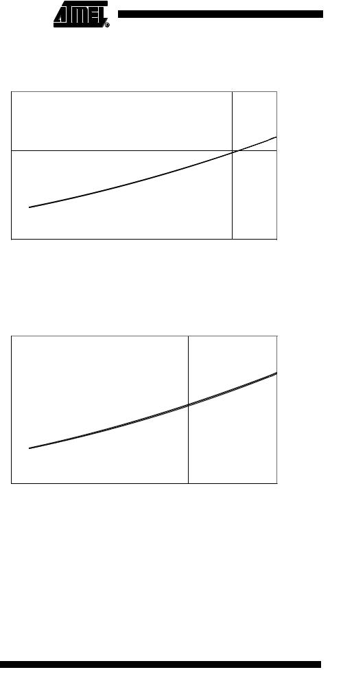
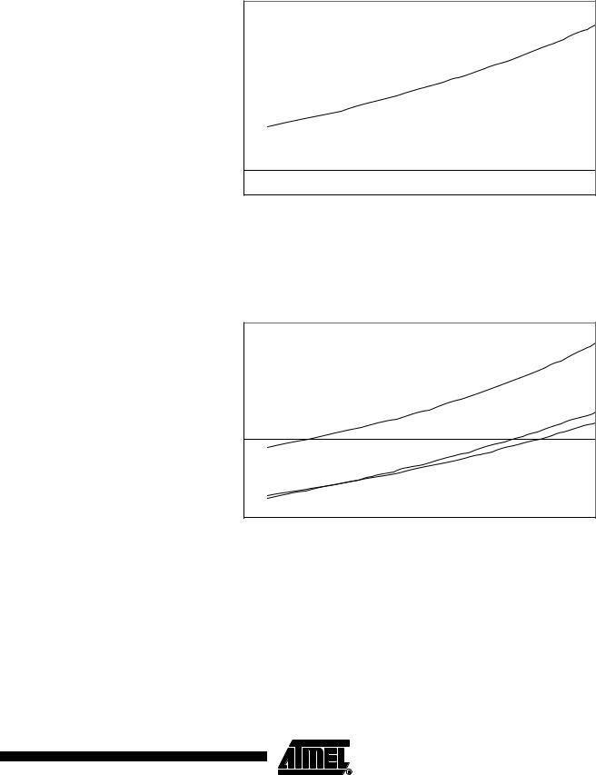
Figure 141. Idle Supply Current vs. VCC (Internal RC Oscillator, 2 MHz)
IDLE SUPPLY CURRENT vs. VCC
INTERNAL RC OSCILLATOR, 2 MHz
2.5
2
-40°C 25°C
85°C
1.5
ICC (mA)
1
0.5
0
2.5 |
3 |
3.5 |
4 |
4.5 |
5 |
5.5 |
VCC (V)
Figure 142. Idle Supply Current vs. VCC (Internal RC Oscillator, 1 MHz)
ICC (mA)
IDLE SUPPLY CURRENT vs. VCC
INTERNAL RC OSCILLATOR, 1 MHz
1.2
1 |
85°C |
|
|
|
25°C |
|
-40°C |
0.8
0.6
0.4
0.2
0
2.5 |
3 |
3.5 |
4 |
4.5 |
5 |
5.5 |
VCC (V)
272 ATmega8535(L)
2502K–AVR–10/06
 ATmega8535(L)
Figure 143. Idle Supply Current vs. VCC (32 kHz External Oscillator)
ICC (mA)
IDLE SUPPLY CURRENT vs. VCC
32kHz EXTERNAL OSCILLATOR
0.04
0.035 |
25°C |
0.03
0.025
0.02
0.015
0.01
0.005
0
2.5 |
3 |
3.5 |
4 |
4.5 |
5 |
5.5 |
VCC (V)
Power-Down Supply Current Figure 144. Power-Down Supply Current vs. VCC (Watchdog Timer Disabled)
ICC (uA)
POWER-DOWN SUPPLY CURRENT vs. VCC
WATCHDOG TIMER DISABLED
2.5
85°C
2
1.5
-40°C
25°C
1
0.5
0
2.5 |
3 |
3.5 |
4 |
4.5 |
5 |
5.5 |
VCC (V)
273
2502K–AVR–10/06
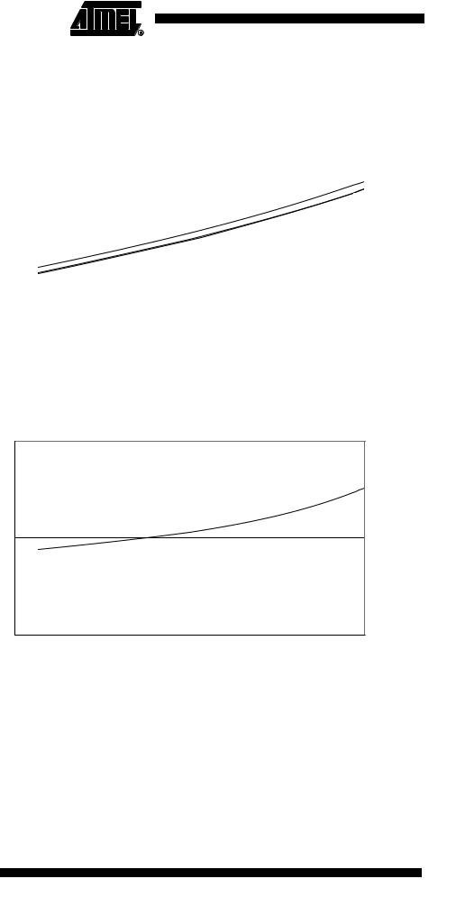
Figure 145. Power-Down Supply Current vs. VCC (Watchdog Timer Enabled)
|
|
|
|
POWER-DOWN SUPPLY CURRENT vs. VCC |
|
|
|
|
|||||
0.025 |
|
|
|
WATCHDOG TIMER ENABLED |
|
|
|
|
|||||
|
|
|
|
|
|
|
|
|
|
|
|
|
|
|
|
|
|
|
|
|
|
|
|
|
|
|
|
0.02 |
|
|
|
|
|
|
|
|
|
|
|
|
85°C |
|
|
|
|
|
|
|
|
|
|
|
|
||
|
|
|
|
|
|
|
|
|
|
|
|
|
|
|
|
|
|
|
|
|
|
|
|
|
|
|
25°C |
0.015 |
|
|
|
|
|
|
|
|
|
|
|
|
-40°C |
|
|
|
|
|
|
|
|
|
|
|
|
||
(mA) |
|
|
|
|
|
|
|
|
|
|
|
|
|
CC |
|
|
|
|
|
|
|
|
|
|
|
|
|
I |
|
|
|
|
|
|
|
|
|
|
|
|
|
0.01 |
|
|
|
|
|
|
|
|
|
|
|
|
|
|
|
|
|
|
|
|
|
|
|
|
|
|
|
0.005 |
|
|
|
|
|
|
|
|
|
|
|
|
|
|
|
|
|
|
|
|
|
|
|
|
|
|
|
0 |
|
|
|
|
|
|
|
|
|
|
|
|
|
|
|
|
|
|
|
|
|
|
|
|
|
|
|
2.5 |
3 |
3.5 |
4 |
4.5 |
5 |
5.5 |
|||||||
|
|
|
|
|
|
VCC (V) |
|
|
|
|
|
|
|
Power-Save Supply Current Figure 146. Power-Save Supply Current vs. VCC (Watchdog Timer Disabled)
ICC (uA)
POWER-SAVE SUPPLY CURRENT vs. VCC
WATCHDOG TIMER DISABLED
16
14
12 |
25°C |
10
8
6
4
2
0
2.5 |
3 |
3.5 |
4 |
4.5 |
5 |
5.5 |
VCC (V)
274 ATmega8535(L)
2502K–AVR–10/06