


ATmega8535(L)
Two-wire Serial Interface Characteristics
Table 112 describes the requirements for devices connected to the Two-wire Serial Bus. The ATmega8535 Two-wire Serial Interface meets or exceeds these requirements under the noted conditions.
Timing symbols refer to Figure 127.
Table 112. Two-wire Serial Bus Requirements
Symbol |
Parameter |
|
|
|
|
|
|
Condition |
Min |
|
Max |
Units |
||
|
|
|
|
|
|
|
|
|
|
|
|
|
|
|
VIL |
Input Low Voltage |
|
|
|
|
|
|
|
|
-0.5 |
|
0.3 VCC |
V |
|
VIH |
Input High Voltage |
|
|
|
|
|
|
|
|
0.7 VCC |
VCC + 0.5 |
V |
||
|
|
|
|
|
|
|
|
|
|
|
|
|
|
|
|
(1) |
Hysteresis of Schmitt Trigger Inputs |
|
|
|
|
|
|
(2) |
– |
V |
|||
Vhys |
|
|
|
|
|
0.05 VCC |
||||||||
|
(1) |
Output Low Voltage |
|
|
|
|
|
3 mA sink current |
0 |
|
0.4 |
V |
||
VOL |
|
|
|
|
|
|
||||||||
|
(1) |
Rise Time for both SDA and SCL |
|
|
|
|
|
20 + 0.1C |
(3)(2) |
300 |
ns |
|||
tr |
|
|
|
|
|
|
|
|
|
|
b |
|
|
|
|
(1) |
Output Fall Time from V |
IHmin |
to V |
ILmax |
|
|
10 pF < C < 400 pF(3) |
20 + 0.1C |
(3)(2) |
250 |
ns |
||
tof |
|
|
|
|
|
|
b |
|
b |
|
|
|||
tSP(1) |
Spikes Suppressed by Input Filter |
|
|
|
|
|
0 |
|
50(2) |
ns |
||||
Ii |
Input Current each I/O Pin |
|
|
|
|
0.1VCC < Vi < 0.9VCC |
-10 |
|
10 |
µA |
||||
|
|
|
|
|
|
|
|
|
|
|
|
|||
C (1) |
Capacitance for each I/O Pin |
|
|
|
|
|
|
– |
|
10 |
pF |
|||
|
i |
|
|
|
|
|
|
|
|
|
|
|
|
|
f |
SCL |
SCL Clock Frequency |
|
|
|
f |
CK |
(4) > max(16f , 250kHz)(5) |
0 |
|
400 |
kHz |
||
|
|
|
|
|
|
|
|
SCL |
|
|
|
|
||
|
|
|
|
|
|
|
|
|
fSCL ≤ 100 kHz |
VCC – 0.4V |
1000ns |
Ω |
||
|
|
|
|
|
|
|
|
|
|
|
---------------------------- |
------------------- |
||
Rp |
Value of Pull-up resistor |
|
|
|
|
|
|
|
|
3mA |
|
Cb |
|
|
|
|
|
|
|
|
fSCL > 100 kHz |
VCC – 0.4V |
300ns |
Ω |
|||||
|
|
|
|
|
|
|
|
|
||||||
|
|
|
|
|
|
|
|
|
|
|
---------------------------- |
--------------- |
||
|
|
|
|
|
|
|
|
|
|
|
3mA |
|
Cb |
|
tHD;STA |
Hold Time (Repeated) START Condition |
|
|
|
fSCL ≤ 100 kHz |
4.0 |
|
– |
µs |
|||||
|
|
|
|
|
|
|
|
|
||||||
|
|
|
fSCL > 100 kHz |
0.6 |
|
– |
µs |
|||||||
|
|
|
|
|
|
|
|
|
|
|||||
|
|
|
|
|
|
|
|
f |
|
≤ 100 kHz(6) |
4.7 |
|
– |
µs |
tLOW |
Low Period of the SCL Clock |
|
|
|
SCL |
|
|
|
|
|
||||
|
|
|
fSCL > 100 kHz(7) |
1.3 |
|
– |
µs |
|||||||
|
|
|
|
|
|
|
|
|
||||||
tHIGH |
High Period of the SCL clock |
|
|
|
|
fSCL ≤ 100 kHz |
4.0 |
|
– |
µs |
||||
|
|
|
|
fSCL > 100 kHz |
0.6 |
|
– |
µs |
||||||
|
|
|
|
|
|
|
|
|
|
|||||
tSU;STA |
Set-up Time for a Repeated START |
|
|
|
fSCL ≤ 100 kHz |
4.7 |
|
– |
µs |
|||||
Condition |
|
|
|
|
|
|
fSCL > 100 kHz |
0.6 |
|
– |
µs |
|||
|
|
|
|
|
|
|
|
|
||||||
|
|
|
|
|
|
|
|
|
|
|||||
tHD;DAT |
Data hoLd Time |
|
|
|
|
|
|
fSCL ≤ 100 kHz |
0 |
|
3.45 |
µs |
||
|
|
|
|
|
|
fSCL > 100 kHz |
0 |
|
0.9 |
µs |
||||
|
|
|
|
|
|
|
|
|
|
|||||
|
|
|
|
|
|
|
|
|
|
|
|
|
|
|
tSU;DAT |
Data Setup Time |
|
|
|
|
|
|
fSCL ≤ 100 kHz |
250 |
|
– |
ns |
||
|
|
|
|
|
|
fSCL > 100 kHz |
100 |
|
– |
ns |
||||
|
|
|
|
|
|
|
|
|
|
|||||
tSU;STO |
Setup Time for STOP Condition |
|
|
|
|
fSCL ≤ 100 kHz |
4.0 |
|
– |
µs |
||||
|
|
|
|
|
|
|
|
|
|
|||||
|
|
|
|
fSCL > 100 kHz |
0.6 |
|
– |
µs |
||||||
|
|
|
|
|
|
|
|
|
|
|||||
tBUF |
Bus Free Time between a STOP and START |
|
|
|
fSCL ≤ 100 kHz |
4.7 |
|
– |
µs |
|||||
Condition |
|
|
|
|
|
|
fSCL > 100 kHz |
1.3 |
|
– |
µs |
|||
|
|
|
|
|
|
|
|
|
||||||
|
|
|
|
|
|
|
|
|
|
|||||
|
|
|
|
|
|
|
|
|
|
|
|
|
|
|
Notes: 1. In ATmega8535, this parameter is characterized and not 100% tested.
2.Required only for fSCL > 100 kHz.
3.Cb = capacitance of one bus line in pF.
259
2502K–AVR–10/06
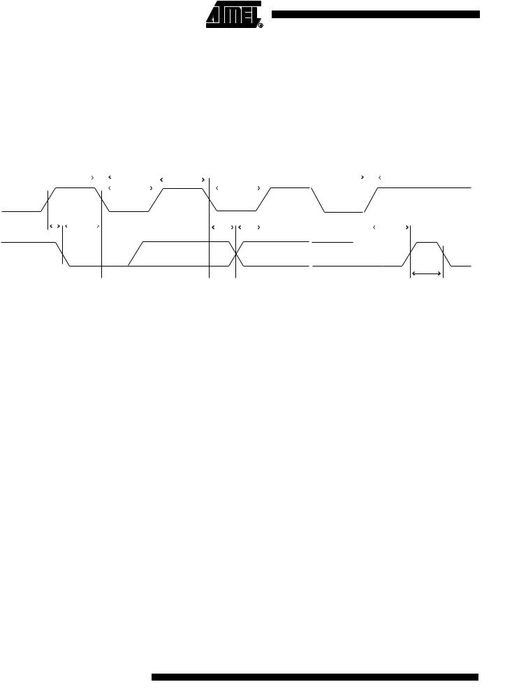
4.fCK = CPU clock frequency.
5.This requirement applies to all ATmega8535 Two-wire Serial Interface operation. Other devices connected to the Two-wire Serial Bus need only obey the general fSCL requirement.
6.The actual low period generated by the ATmega8535 Two-wire Serial Interface is (1/fSCL - 2/fCK), thus fCK must be greater than 6 MHz for the low time requirement to be strictly met at fSCL = 100 kHz.
7.The actual low period generated by the ATmega8535 Two-wire Serial Interface is (1/fSCL - 2/fCK), thus the low time requirement will not be strictly met for fSCL > 308 kHz when fCK = 8 MHz. Still, ATmega8535 devices connected to the bus may communicate at full speed (400 kHz) with other ATmega8535 devices, as well as any other device with a proper tLOW acceptance margin.
Figure 127. Two-wire Serial Bus Timing
|
|
|
|
|
|
|
|
|
|
tof |
|
|
tHIGH |
|
|
|
|
|
|
|
|
|
|
|
|
|
|
|
|
tr |
||
|
|
|
|
|
|
|
|
|
|
|
||||||||||||||||||||||
|
|
|
|
|
|
|
|
|
|
|
|
|
|
|
|
|
|
|
|
|||||||||||||
SCL |
|
|
|
|
|
|
|
|
|
tLOW |
|
|
|
|
tLOW |
|
|
|
|
|
|
|
|
|
|
|
|
|
||||
|
|
|
|
|
|
|
|
|
|
|
||||||||||||||||||||||
|
|
|
|
|
|
|
|
|
|
|
|
|
|
|
|
|
|
|
|
|
|
|
|
|
|
|
|
|
|
|
|
|
|
|
|
|
|
|
|
|
|
|
|
|
|
|
|
|
|
|
|
|
|
|
|
|
|
|
|
|
|
|
|
|
|
tSU;STA |
|
|
|
|
|
|
|
tHD;STA |
|
tHD;DAT |
|
|
|
|
|
|
t |
|
|
|
|
|
|
|
||||||||
|
|
|
|
|
||||||||||||||||||||||||||||
|
|
|
|
|
|
|
|
|
|
|
|
|
|
|
|
|
|
|
||||||||||||||
SDA |
|
|
|
|
|
|
|
|
|
|
|
|
|
|
|
|
|
|
|
|
SU;DAT |
|
|
|
|
tSU;STO |
||||||
|
|
|
|
|
|
|
|
|
|
|
|
|
|
|
|
|
|
|
|
|
|
|
|
|
|
|
|
|
||||
|
|
|
|
|
|
|
|
|
|
|
|
|
|
|
|
|
|
|
|
|
|
|
|
|
|
|
|
|
|
|
|
|
tBUF
260 ATmega8535(L)
2502K–AVR–10/06
 ATmega8535(L)
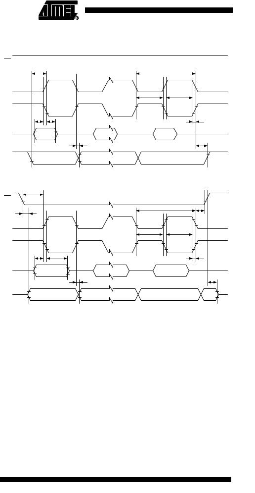
Figure 128. SPI Interface Timing Requirements (Master Mode)
SS
6 |
|
1 |
SCK |
|
|
|
|
(CPOL = 0) |
|
|
|
|
|
|
2 |
2 |
|
SCK |
|
|
|
|
(CPOL = 1) |
|
|
|
|
4 |
5 |
|
3 |
|
MISO |
MSB |
... |
LSB |
|
(Data Input) |
||||
|
|
|
||
|
|
7 |
8 |
|
MOSI |
MSB |
... |
LSB |
|
(Data Output) |
||||
|
|
|
Figure 129. SPI Interface Timing Requirements (Slave Mode)
18 |
|
|
|
|
|
SS |
|
|
|
|
|
9 |
|
|
10 |
16 |
|
|
|
|
|
||
SCK |
|
|
|
|
|
(CPOL = 0) |
|
|
|
|
|
|
|
11 |
11 |
|
|
SCK |
|
|
|
|
|
(CPOL = 1) |
|
|
|
|
|
13 |
14 |
|
|
12 |
|
MOSI |
MSB |
... |
LSB |
|
|
(Data Input) |
|
||||
|
|
|
|
||
|
|
15 |
|
17 |
|
MISO |
MSB |
... |
LSB |
X |
|
(Data Output) |
|||||
|
|
|
|
262 ATmega8535(L)
2502K–AVR–10/06