

4.35 A commercial sem. (Courtesy of Hitachi Scientific Instruments.)
The secondary electron beam signal is displayed on a TV screen in a scanning pattern synchronized with the electron beam scan of the sample surface.
The magnification possible with the SEM is limited by the beam spot size and is considerably better than that possible with the optical microscope with the optical microscope but less than that possible with the TEM.
Important feature of an SEM image is that it looks like a visual image of a large-scale piece.
SEM is especially useful for convenient inspections of grain structure.
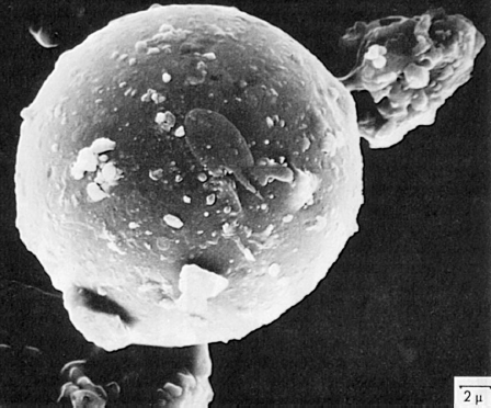
Fig.4.36. SEM image of a 23-μm-diameter lunar rock from the Apollo 11 mission. The SEM gives an image with “depth” in contrast to optical micrographs. The spherical shape indicates a prior melting process.

Fig.4.37. SEM image of a metal (type 304 stainless steel) fracture surface, 180x.
(a) (b) (c)
Fig.4.38. (a) SEM image of the topography of a lead-tin solder alloy with lead-rich and tin rich regions. (b) A map of the same area shown in (a) indicating the lead distribution (light area) in the microstructure. The light area corresponds to regions emitting characteristic lead x-rays when struck by the scanning electron beam. (c) A similar map of the tin distribution (light area) in the microstructure.
Atomic resolution electron microscope
Resolution for this instrument is about 0.1 nm.
Scanning tunneling microscope (STM)
The first is in a new instrument capable of providing direct images of individual atomic packing patterns.
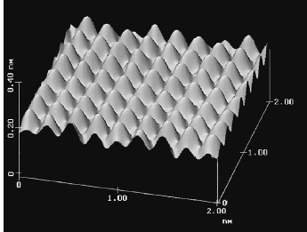
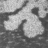
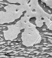
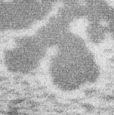
Fig.4.39. Scanning tunneling micrograph of an interstitial atom defect on the surface of graphite.
Explanation for basis image in the STM
The name of STM comes from the x-y raster (scanning) by a sharp metal tip near the surface of a conducting sample, leading to a measurable electrical current due to the quantum – mechanical tunneling of electrons near the surface.
For gap distance around 0.5 nm, an applied bias of tens of mV leads to nanoampere current flow.
The needle’s vertical distance (z-direction) above the surface is continually adjusted to maintain a constant tunnel current.
The surface topography is the record of the trajectory of the tip.
Atomic force microscope (AFM)
Explanation for basis image in the AFM
AFM is based on the concept that the atomic surface should be resolvable, using a force as well as a current. This hypothesis was confirmed by demonstrating that a small cantilever can be constructed to have a spring constant weaker than the equivalent spring between adjacent atoms.

Fig.4.40. Schematic of the principle by which the probe tip of either a scanning tunneling microscope (STM) or an atomic force microscope (AFM) operates. The sharp tip follows the contour A-A as it maintains either a constant tunneling current (in the STM) or a constant force (in the AFM). The STM requires a conductive sample while the AFM can also inspect insulators.
Example:
The interatomic force constant is typically 1 N/m, similar in value to that for a piece of common Al foil 4 mm long and 1 mm wide. This mechanical equivalence permits a sharp tip to image both conducting and nonconducting materials.
Remember:
STM – for conductive sample;
AFM – for conducting and nonconducting materials.
Conclusion
When the impurity, or solute, atoms are similar to the solvent atoms, substitutional solution takes place in which impurity atoms rest on crystal lattice sites.
Interstitial solution takes place when a solute atom is small enough to occupy open spaces among adjacent atoms in the crystal structure. Solid solution in ionic compounds must account for charge neutrality of the material as a whole.
Point defects can be missing atoms or ions (vacancies) or extra atoms or ions (interstitialcies). Charge neutrality must be maintained locally for point defect structures in ionic compounds.
Linear defects or dislocations, correspond to an extra half-plane of atoms in an otherwise perfect crystal. Although dislocation structures can be complex, they can also be characterized with simple parameters, the Burgers vector.
Planar defects include any boundary surface surroundings a crystalline structure. Twin boundaries divide 2 mirror-image regions. The exterior surface has a characteristic structure involving an elaborate ledge system.
The predominant microstructural feature for many engineering materials is grain structure, where each grain is a region with a characteristic crystal structure orientation.
A grain-size number (G) is used to quantify this microstructure. The structure of the region of mismatch between adjacent grains (i.e., the grain boundary) depends on the relative orientation of the grains.
Noncrystalline solids, on the atomic scale, are lacking in any long-range order (LRO) but may exhibit short-range order (SRO) associated with structural building blocks such as SiO4-4 tetrahedra.
Quasicrystals represent an intermediate state between crystals and glasses. Their fivefold symmetry diffraction patterns are the result of orientation order on the absence of translation periodicity.
The icosahedral phases have been described as 3-dimensional Penrose tilings.
Optical and electron microscopy are powerful tools for observing structural order and disorder.
TEM uses diffraction contrast to obtain high-magnification (e.g., 100000 x) images of defects such as dislocations.
SEM produces 3-dimensional- appearing images of microstructural features such as fracture surface.
STM and AFM provide direct images of individual atomic stacking patterns.