

4.8 Microscopy
We can see grains photo (grain structure, taken with an optical microscope) – as an example of a common and important experimental inspection of an engineering material. The first such inspection was made in 1863 by H.C. Sorby. Optical microscope is familiar to you. Less familiar is the electron microscope. We discussed with you about X-ray diffraction as a tool for measuring ideal crystalline structure. Electron microscope is a standard tool for characterizing the microstructural features.
4.8.1 Electron microscope
Transmission electron microscope: (TEM) is similar to design to a conventional optical microscope except that instead of a beam of light focused by glass lenses, there is a beam of electrons focused by electromagnets (Fig. 4.32).

(c)
Fig.4.32. Similarity in design between (a) an optical microscope and
(b) a transmission electron microscope. The electron microscope uses solenoid coils to produce a magnetic lens in place of the glass lens in the optical microscope,
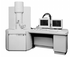
(c) A commercial TEM.
Remember:
This is possible due to the wavelike nature of the electron.
For a typical TEM operating at a constant voltage of 100 keV, electron beam has a monochromatic wavelength λ = 3.7 x 10 –3 nm. (this is 5 orders of magnitude smaller than the wavelength of visible light = 400-700 nm) in optical microscopy.
Result = substantially smaller structural details can be resolved by the TEM compared with the optical microscope.
Practical magnifications in optical microscope = 2000 x
(corresponding to a resolution of structural dimensions as small as about 0.25 μm); for TEM – magnifications = 100000 x ( resolution about 1 nm)
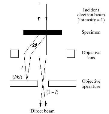
Fig.4.33. The basis of image formation in the TEM is diffraction contrast. Structural variations in the sample cause different fractions (I) of the incident beam
to be diffracted out, giving variations in image darkness at a final viewing screen.
Explanation for basis image in the TEM
The image in TEM is the result of diffraction contrast.
The sample is oriented so that some of the beam is transmitted and some is diffracted.
Any local variation in crystalline regularity will cause a different fraction of the incident beam intensity to be “diffracted out”, leading to a variation in image darkness on a viewing screen at the base of the microscope (Fig.4.34).

(a) (b)
(c)
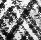
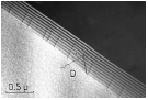
Fig.4.34. (a) TEM image of the strain field around small dislocation loops in a zirconium alloy. These loops result from a condensation of point defects (either interstitial atoms or vacancies) after neutron irradiation. (b) Forest of dislocations in a stainless steel as seen by a TEM. (c)TEM image of a grain boundary. The parallel lines identify the boundary. A dislocation intersecting the boundary is labeled D.
4.8.2 Scanning electron microscope (sem)
SEM obtains structural images by an entirely different method than that used by the TEM.
Explanation for basis image in the SEM
An electron beam spot ~ 1 μm in diameter is scanned repeatedly over the surface of the sample. Slight variation in surface topography produce marked variations in the strength of the beam of secondary electrons – electrons ejected from the surface of the sample by the force of collision with primary electrons from the electron beam.
