

3 Linear defects, or dislocations – one-dimensional imperfection
We have seen that point (zero-dimensional) defects are structural imperfections resulting from thermal agitation. Linear defects, which are one-dimensional, are associated primarily with mechanical deformation. Linear defects are also known as dislocations.
4 Planar defects – two-dimensional imperfections
There are various forms of planar defects.
Fig.8 shows a twin boundary which separates 2 crystalline regions that are, structurally, mirror images of each other.
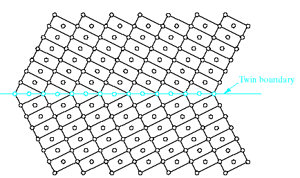
Fig.8. A twin boundary separates 2 crystalline regions that are, structurally, mirror images of each other.
The most important planar defect for our consideration in this introductory course occurs at the grain boundary, the region between 2 adjacent single crystals, or grains.
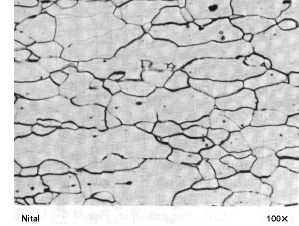
Fig. 9. Typical optical micrograph of a grain structure, 100x.
The grain boundaries (Fig.9) have been lightly etched with chemical solutions so, that they reflect light differently from the polished grains, thereby giving a distinctive contrast.
5 Microscopy
We can see grains photo (grain structure, taken with an optical microscope) – as an example of a common and important experimental inspection of an engineering material. The first such inspection was made in 1863 by H.C. Sorby. Optical microscope is familiar to you. Less familiar is the electron microscope. We discussed with you about X-ray diffraction as a tool for measuring ideal crystalline structure. Electron microscope is a standard tool for characterizing the microstructural features.
5.1 Electron microscope
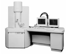
Transmission electron microscope: (TEM) is similar to design to a conventional optical microscope except that instead of a beam of light focused by glass lenses, there is a beam of electrons focused by electromagnets (Fig. 10).
(c)
Fig.10. Commercial TEM.
Remember:
This is possible due to the wavelike nature of the electron.
For a typical TEM operating at a constant voltage of 100 keV, electron beam has a monochromatic wavelength λ = 3.7 x 10 –3 nm. (this is 5 orders of magnitude smaller than the wavelength of visible light = 400-700 nm) in optical microscopy.
Result = substantially smaller structural details can be resolved by the TEM compared with the optical microscope.
Practical magnifications in optical microscope = 2000 x
(corresponding to a resolution of structural dimensions as small as about 0.25 μm); for TEM – magnifications = 100000 x ( resolution about 1 nm)
5.2 Scanning electron microscope (sem)
SEM obtains structural images by an entirely different method than that used by the TEM.
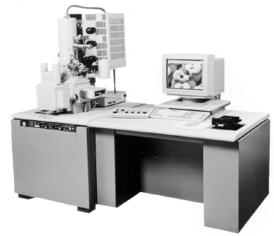
Fig.11. Commercial SEM. (Courtesy of Hitachi Scientific Instruments.)
Explanation for basis image in the SEM
An electron beam spot ~ 1 μm in diameter is scanned repeatedly over the surface of the sample. Slight variation in surface topography produce marked variations in the strength of the beam of secondary electrons – electrons ejected from the surface of the sample by the force of collision with primary electrons from the electron beam.
The secondary electron beam signal is displayed on a TV screen in a scanning pattern synchronized with the electron beam scan of the sample surface.
The magnification possible with the SEM is limited by the beam spot size and is considerably better than that possible with the optical microscope with the optical microscope but less than that possible with the TEM.
Important feature of an SEM image is that it looks like a visual image of a large-scale piece.
SEM is especially useful for convenient inspections of grain structure.
Atomic resolution electron microscope Resolution for this instrument is about 0.1 nm.
Scanning tunneling microscope (STM)
The first is in a new instrument capable of providing direct images of individual atomic packing patterns.
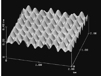
Fig.12. Scanning tunneling micrograph of an interstitial atom defect on the surface of graphite.
Explanation for basis image in the STM
The name of STM comes from the x-y raster (scanning) by a sharp metal tip near the surface of a conducting sample, leading to a measurable electrical current due to the quantum – mechanical tunneling of electrons near the surface.
For gap distance around 0.5 nm, an applied bias of tens of mV leads to nanoampere current flow.
The needle’s vertical distance (z-direction) above the surface is continually adjusted to maintain a constant tunnel current. The surface topography is the record of the trajectory of the tip.
Atomic force microscope (AFM)
AFM is based on the concept that the atomic surface should be resolvable, using a force as well as a current. This hypothesis was confirmed by demonstrating that a small cantilever can be constructed to have a spring constant weaker than the equivalent spring between adjacent atoms.
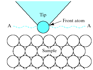
Fig.13. Schematic of the principle by which the probe tip of either a scanning tunneling microscope (STM) or an atomic force microscope (AFM) operates. The sharp tip follows the contour A-A as it maintains either a constant tunneling current (in the STM) or a constant force (in the AFM). The STM requires a conductive sample while the AFM can also inspect insulators.
Conclusion
When the impurity, or solute, atoms are similar to the solvent atoms, substitutional solution takes place in which impurity atoms rest on crystal lattice sites.
Interstitial solution takes place when a solute atom is small enough to occupy open spaces among adjacent atoms in the crystal structure. Solid solution in ionic compounds must account for charge neutrality of the material as a whole.
Point defects can be missing atoms or ions (vacancies) or extra atoms or ions (interstitialcies). Charge neutrality must be maintained locally for point defect structures in ionic compounds.
Linear defects or dislocations, correspond to an extra half-plane of atoms in an otherwise perfect crystal. Although dislocation structures can be complex, they can also be characterized with simple parameters, the Burgers vector.
Planar defects include any boundary surface surroundings a crystalline structure. Twin boundaries divide 2 mirror-image regions. The exterior surface has a characteristic structure involving an elaborate ledge system.
The predominant microstructural feature for many engineering materials is grain structure, where each grain is a region with a characteristic crystal structure orientation.
A grain-size number (G) is used to quantify this microstructure. The structure of the region of mismatch between adjacent grains (i.e., the grain boundary) depends on the relative orientation of the grains.
Noncrystalline solids, on the atomic scale, are lacking in any long-range order (LRO) but may exhibit short-range order (SRO) associated with structural building blocks such as SiO4-4 tetrahedra.
Quasicrystals represent an intermediate state between crystals and glasses. Their fivefold symmetry diffraction patterns are the result of orientation order on the absence of translation periodicity.
The icosahedral phases have been described as 3-dimensional Penrose tilings.
Optical and electron microscopy are powerful tools for observing structural order and disorder.
TEM uses diffraction contrast to obtain high-magnification (e.g., 100000 x) images of defects such as dislocations.
SEM produces 3-dimensional- appearing images of microstructural features such as fracture surface.
STM and AFM provide direct images of individual atomic stacking patterns.