- •Preface
- •About this document
- •Feedback
- •1 Introduction to the AMBA Buses
- •1.1 Overview of the AMBA specification
- •1.1.2 Advanced System Bus (ASB)
- •1.1.3 Advanced Peripheral Bus (APB)
- •1.2 Objectives of the AMBA specification
- •1.4 Terminology
- •1.5 Introducing the AMBA AHB
- •1.6 Introducing the AMBA ASB
- •1.7 Introducing the AMBA APB
- •1.8 Choosing the right bus for your system
- •1.8.1 Choice of system bus
- •1.8.2 System bus and peripheral bus
- •1.8.3 When to use AMBA AHB/ASB or APB
- •1.9 Notes on the AMBA specification
- •1.9.1 Technology independence
- •1.9.2 Electrical characteristics
- •1.9.3 Timing specification
- •2 AMBA Signals
- •2.1 AMBA signal names
- •2.1.1 AHB signal prefixes
- •2.1.2 ASB signal prefixes
- •2.1.3 APB signal prefixes
- •2.2 AMBA AHB signal list
- •2.3 AMBA ASB signal list
- •2.4 AMBA APB signal list
- •3 AMBA AHB
- •3.1 About the AMBA AHB
- •3.2 Bus interconnection
- •3.3 Overview of AMBA AHB operation
- •3.4 Basic transfer
- •3.5 Transfer type
- •3.6 Burst operation
- •3.6.1 Early burst termination
- •3.7 Control signals
- •3.7.1 Transfer direction
- •3.7.2 Transfer size
- •3.7.3 Protection control
- •3.8 Address decoding
- •3.9 Slave transfer responses
- •3.9.1 Transfer done
- •3.9.2 Transfer response
- •3.9.4 Error response
- •3.9.5 Split and retry
- •3.10 Data buses
- •3.10.1 HWDATA[31:0]
- •3.10.2 HRDATA[31:0]
- •3.10.3 Endianness
- •3.11 Arbitration
- •3.11.1 Signal description
- •3.11.2 Requesting bus access
- •3.11.3 Granting bus access
- •3.11.4 Early burst termination
- •3.11.5 Locked transfers
- •3.11.6 Default bus master
- •3.12 Split transfers
- •3.12.1 Split transfer sequence
- •3.12.2 Multiple split transfers
- •3.12.3 Preventing deadlock
- •3.12.4 Bus handover with split transfers
- •3.13 Reset
- •3.14 About the AHB data bus width
- •3.15 Implementing a narrow slave on a wider bus
- •3.16 Implementing a wide slave on a narrow bus
- •3.16.1 Masters
- •3.17 About the AHB AMBA components
- •3.18 AHB bus slave
- •3.18.1 Interface diagram
- •3.18.2 Timing diagrams
- •3.18.3 Timing parameters
- •3.19 AHB bus master
- •3.19.1 Interface diagram
- •3.19.2 Bus master timing diagrams
- •3.19.3 Timing parameters
- •3.20 AHB arbiter
- •3.20.1 Interface diagram
- •3.20.2 Timing diagrams
- •3.20.3 Timing parameters
- •3.21 AHB decoder
- •3.21.1 Interface diagram
- •3.21.2 Timing diagram
- •3.21.3 Timing parameter
- •4 AMBA ASB
- •4.1 About the AMBA ASB
- •4.1.2 AMBA ASB and APB
- •4.2 AMBA ASB description
- •4.3 ASB transfers
- •4.3.1 Nonsequential transfer
- •4.3.2 Sequential transfer
- •4.4 Address decode
- •4.5 Transfer response
- •4.6.1 Arbiter
- •4.6.2 Bus master handover
- •4.6.3 Default bus master
- •4.6.4 Locked transfers
- •4.7 Reset operation
- •4.7.1 Exit from reset
- •4.8 Description of ASB signals
- •4.8.1 Clock
- •4.8.2 Reset
- •4.8.3 Transfer type
- •4.8.4 Address and control information
- •4.8.5 Address bus
- •4.8.6 Transfer direction
- •4.8.7 Transfer size
- •4.8.8 Protection information
- •4.8.9 Address and control signal timing
- •4.8.10 Tristate enable of address and control signals
- •4.8.11 Slave select signals
- •4.8.12 Transfer response
- •4.8.13 Data bus
- •4.8.14 Arbitration signals
- •4.9 About the ASB AMBA components
- •4.10 ASB bus slave
- •4.10.1 Interface diagram
- •4.10.2 Bus slave interface description
- •4.10.3 Timing diagrams
- •4.10.4 Timing parameters
- •4.11 ASB bus master
- •4.11.1 Interface diagram
- •4.11.2 Bus master interface description
- •4.11.3 Bus interface state machine
- •4.11.4 Bus master timing diagrams
- •4.11.5 Timing parameters
- •4.12 ASB decoder
- •4.12.1 Interface diagram
- •4.12.2 Decoder description
- •4.12.3 Timing diagrams
- •4.12.4 Timing parameters
- •4.13 ASB arbiter
- •4.13.1 Interface diagram
- •4.13.2 Arbiter description
- •4.13.3 Timing diagrams
- •4.13.4 Timing parameters
- •5 AMBA APB
- •5.1 About the AMBA APB
- •5.2 APB specification
- •5.2.1 State diagram
- •5.2.2 Write transfer
- •5.2.3 Read transfer
- •5.3 About the APB AMBA components
- •5.4 APB bridge
- •5.4.1 Interface diagram
- •5.4.2 APB bridge description
- •5.4.3 Timing diagrams
- •5.4.4 Timing parameters
- •5.5 APB slave
- •5.5.1 Interface diagram
- •5.5.2 APB slave description
- •5.5.3 Timing diagrams
- •5.5.4 Timing parameters
- •5.6 Interfacing APB to AHB
- •5.6.1 Read transfers
- •5.6.2 Write transfers
- •5.6.3 Back to back transfers
- •5.6.4 Tristate data bus implementations
- •5.7 Interfacing APB to ASB
- •5.7.1 Write transfer
- •5.7.2 Read transfer
- •5.8 Interfacing rev D APB peripherals to rev 2.0 APB
- •6 AMBA Test Methodology
- •6.1 About the AMBA test interface
- •6.2 External interface
- •6.2.1 Test bus request A
- •6.2.2 Test bus request B
- •6.2.3 Test acknowledge
- •6.2.4 Test clock
- •6.2.5 Test bus
- •6.3 Test vector types
- •6.4 Test interface controller
- •6.4.1 Test transfer parameters
- •6.4.2 Incremental addressing
- •6.4.3 Entering test mode
- •6.4.4 Address vectors
- •6.4.5 Control vector
- •6.4.6 Write test vectors
- •6.4.7 Read test vectors
- •6.4.8 Burst vectors
- •6.4.9 Changing a burst direction
- •6.4.10 Exiting test mode
- •6.5 The AHB Test Interface Controller
- •6.5.1 Control vector
- •6.6 Example AMBA AHB test sequences
- •6.6.1 Entering test mode
- •6.6.2 Write test vectors
- •6.6.3 Read transfers
- •6.6.4 Control vector
- •6.6.5 Burst vectors
- •6.6.7 Exiting test mode
- •6.7 The ASB test interface controller
- •6.7.1 Control vector bit definitions
- •6.8 Example AMBA ASB test sequences
- •6.8.1 Entering test mode
- •6.8.2 Address vectors
- •6.8.3 Control vectors
- •6.8.4 Write test vectors
- •6.8.5 Changing burst direction
- •6.8.6 Exiting test mode
AMBA Test Methodology
6.8.4Write test vectors
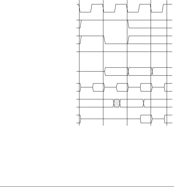
Figure 6-14 shows an example of a single write vector following a single address vector.
|
C0 |
C1 |
C2 |
TCLK |
|
|
|
TREQA |
|
|
|
TREQB |
|
|
|
TACK |
|
|
|
TBUS |
|
Address |
Write 1 |
|
vector |
vector |
|
|
|
||
BTRAN[1:0] |
A-TRAN |
N-TRAN |
|
BA |
|
|
A |
BD |
|
|
Write |
|
|
data |
|
|
|
|
Figure 6-14 Write test vectors
ARM IHI 0011A |
© Copyright ARM Limited 1999. All rights reserved. |
6-31 |
AMBA Test Methodology
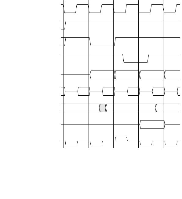
Figure 6-15 shows an example of extended write vectors following a single address
vector. |
|
|
|
|
|
C0 |
C1 |
C2 |
C3 |
TCLK |
|
|
|
|
TREQA |
|
|
|
|
TREQB |
|
|
|
|
TACK |
|
|
|
|
TBUS |
|
Address |
Write |
Write |
|
vector |
vector |
vector |
|
|
|
|||
BTRAN[1:0] |
A-TRAN |
N-TRAN |
|
|
BA |
|
|
A |
|
BD |
|
|
|
Write |
|
|
|
data |
|
|
|
|
|
|
BWAIT |
|
|
|
|
Figure 6-15 Extended write test vectors
6-32 |
© Copyright ARM Limited 1999. All rights reserved. |
ARM IHI 0011A |
AMBA Test Methodology
Figure 6-16 shows an example of a single address vector, followed by a single read vector and terminated with a single turnaround vector.
|
C0 |
C1 |
C2 |
C3 |
C4 |
TCLK |
|
|
|
|
|
TREQA |
|
|
|
|
|
TREQB |
|
|
|
|
|
TACK |
|
|
|
|
|
TBUS |
|
Address |
|
Read |
|
|
vector |
|
vector |
|
|
|
|
|
|
||
BTRAN[1:0] |
A-TRAN |
N-TRAN |
|
A-TRAN |
|
BA |
|
|
A |
|
|
BD |
|
|
|
Read |
|
|
|
|
data 1 |
|
|
|
|
|
|
|
Figure 6-16 Read test vector
ARM IHI 0011A |
© Copyright ARM Limited 1999. All rights reserved. |
6-33 |
AMBA Test Methodology
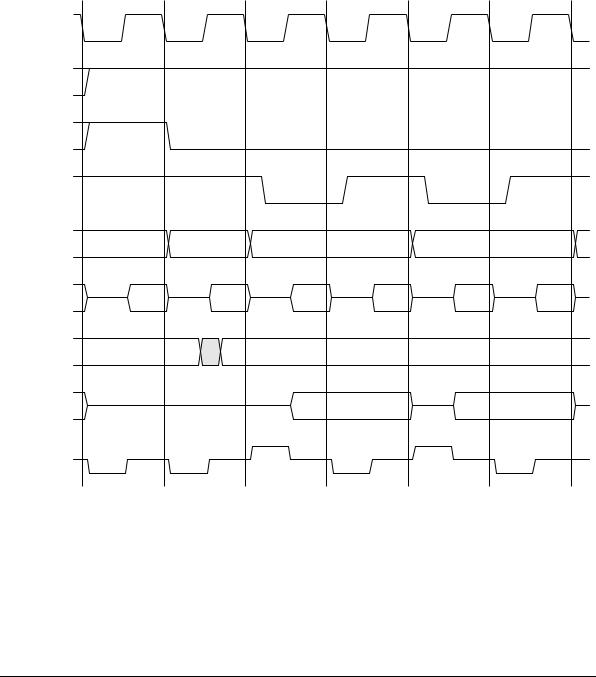
Figure 6-17 shows SEQUENTIAL transfers to non-incrementing addresses.
C0 |
C1 |
C2 |
C3 |
C4 |
C5 |
TCLK
TREQA |
|
|
|
|
|
|
TREQB |
|
|
|
|
|
|
TACK |
|
|
|
|
|
|
TBUS |
|
Address |
Write 1 |
|
Write 2 |
|
|
vector |
vector |
|
vector |
|
|
|
|
|
|
|||
BTRAN[1:0] |
A-TRAN |
N-TRAN |
N-TRAN |
N-TRAN |
N-TRAN |
N-TRAN |
BA |
|
|
A |
|
|
|
BD |
|
|
Write 1 |
|
Write 2 |
|
|
|
data |
|
data |
|
|
|
|
|
|
|
BWAIT
Figure 6-17 Burst write vectors with increment disabled
6-34 |
© Copyright ARM Limited 1999. All rights reserved. |
ARM IHI 0011A |
AMBA Test Methodology
Figure 6-18 shows SEQUENTIAL transfers to incrementing addresses.
|
C0 |
C1 |
C2 |
C3 |
C4 |
C5 |
TCLK |
|
|
|
|
|
|
TREQA |
|
|
|
|
|
|
TREQB |
|
|
|
|
|
|
TACK |
|
|
|
|
|
|
TBUS |
|
Address |
Write 1 |
Write 2 |
Write 3 |
Write 4 |
|
vector |
vector |
vector |
vector |
vector |
|
|
|
|||||
BTRAN[1:0] |
A-TRAN |
N-TRAN |
S-TRAN |
S-TRAN |
S-TRAN |
S-TRAN |
BA |
|
|
A |
A + 4 |
A + 8 |
A + 12 |
BD |
|
|
Write 1 |
Write 2 |
Write 3 |
Write 4 |
|
|
data |
data |
data |
data |
|
|
|
|
Figure 6-18 Burst write vectors with increment enabled
ARM IHI 0011A |
© Copyright ARM Limited 1999. All rights reserved. |
6-35 |