- •Preface
- •About this document
- •Feedback
- •1 Introduction to the AMBA Buses
- •1.1 Overview of the AMBA specification
- •1.1.2 Advanced System Bus (ASB)
- •1.1.3 Advanced Peripheral Bus (APB)
- •1.2 Objectives of the AMBA specification
- •1.4 Terminology
- •1.5 Introducing the AMBA AHB
- •1.6 Introducing the AMBA ASB
- •1.7 Introducing the AMBA APB
- •1.8 Choosing the right bus for your system
- •1.8.1 Choice of system bus
- •1.8.2 System bus and peripheral bus
- •1.8.3 When to use AMBA AHB/ASB or APB
- •1.9 Notes on the AMBA specification
- •1.9.1 Technology independence
- •1.9.2 Electrical characteristics
- •1.9.3 Timing specification
- •2 AMBA Signals
- •2.1 AMBA signal names
- •2.1.1 AHB signal prefixes
- •2.1.2 ASB signal prefixes
- •2.1.3 APB signal prefixes
- •2.2 AMBA AHB signal list
- •2.3 AMBA ASB signal list
- •2.4 AMBA APB signal list
- •3 AMBA AHB
- •3.1 About the AMBA AHB
- •3.2 Bus interconnection
- •3.3 Overview of AMBA AHB operation
- •3.4 Basic transfer
- •3.5 Transfer type
- •3.6 Burst operation
- •3.6.1 Early burst termination
- •3.7 Control signals
- •3.7.1 Transfer direction
- •3.7.2 Transfer size
- •3.7.3 Protection control
- •3.8 Address decoding
- •3.9 Slave transfer responses
- •3.9.1 Transfer done
- •3.9.2 Transfer response
- •3.9.4 Error response
- •3.9.5 Split and retry
- •3.10 Data buses
- •3.10.1 HWDATA[31:0]
- •3.10.2 HRDATA[31:0]
- •3.10.3 Endianness
- •3.11 Arbitration
- •3.11.1 Signal description
- •3.11.2 Requesting bus access
- •3.11.3 Granting bus access
- •3.11.4 Early burst termination
- •3.11.5 Locked transfers
- •3.11.6 Default bus master
- •3.12 Split transfers
- •3.12.1 Split transfer sequence
- •3.12.2 Multiple split transfers
- •3.12.3 Preventing deadlock
- •3.12.4 Bus handover with split transfers
- •3.13 Reset
- •3.14 About the AHB data bus width
- •3.15 Implementing a narrow slave on a wider bus
- •3.16 Implementing a wide slave on a narrow bus
- •3.16.1 Masters
- •3.17 About the AHB AMBA components
- •3.18 AHB bus slave
- •3.18.1 Interface diagram
- •3.18.2 Timing diagrams
- •3.18.3 Timing parameters
- •3.19 AHB bus master
- •3.19.1 Interface diagram
- •3.19.2 Bus master timing diagrams
- •3.19.3 Timing parameters
- •3.20 AHB arbiter
- •3.20.1 Interface diagram
- •3.20.2 Timing diagrams
- •3.20.3 Timing parameters
- •3.21 AHB decoder
- •3.21.1 Interface diagram
- •3.21.2 Timing diagram
- •3.21.3 Timing parameter
- •4 AMBA ASB
- •4.1 About the AMBA ASB
- •4.1.2 AMBA ASB and APB
- •4.2 AMBA ASB description
- •4.3 ASB transfers
- •4.3.1 Nonsequential transfer
- •4.3.2 Sequential transfer
- •4.4 Address decode
- •4.5 Transfer response
- •4.6.1 Arbiter
- •4.6.2 Bus master handover
- •4.6.3 Default bus master
- •4.6.4 Locked transfers
- •4.7 Reset operation
- •4.7.1 Exit from reset
- •4.8 Description of ASB signals
- •4.8.1 Clock
- •4.8.2 Reset
- •4.8.3 Transfer type
- •4.8.4 Address and control information
- •4.8.5 Address bus
- •4.8.6 Transfer direction
- •4.8.7 Transfer size
- •4.8.8 Protection information
- •4.8.9 Address and control signal timing
- •4.8.10 Tristate enable of address and control signals
- •4.8.11 Slave select signals
- •4.8.12 Transfer response
- •4.8.13 Data bus
- •4.8.14 Arbitration signals
- •4.9 About the ASB AMBA components
- •4.10 ASB bus slave
- •4.10.1 Interface diagram
- •4.10.2 Bus slave interface description
- •4.10.3 Timing diagrams
- •4.10.4 Timing parameters
- •4.11 ASB bus master
- •4.11.1 Interface diagram
- •4.11.2 Bus master interface description
- •4.11.3 Bus interface state machine
- •4.11.4 Bus master timing diagrams
- •4.11.5 Timing parameters
- •4.12 ASB decoder
- •4.12.1 Interface diagram
- •4.12.2 Decoder description
- •4.12.3 Timing diagrams
- •4.12.4 Timing parameters
- •4.13 ASB arbiter
- •4.13.1 Interface diagram
- •4.13.2 Arbiter description
- •4.13.3 Timing diagrams
- •4.13.4 Timing parameters
- •5 AMBA APB
- •5.1 About the AMBA APB
- •5.2 APB specification
- •5.2.1 State diagram
- •5.2.2 Write transfer
- •5.2.3 Read transfer
- •5.3 About the APB AMBA components
- •5.4 APB bridge
- •5.4.1 Interface diagram
- •5.4.2 APB bridge description
- •5.4.3 Timing diagrams
- •5.4.4 Timing parameters
- •5.5 APB slave
- •5.5.1 Interface diagram
- •5.5.2 APB slave description
- •5.5.3 Timing diagrams
- •5.5.4 Timing parameters
- •5.6 Interfacing APB to AHB
- •5.6.1 Read transfers
- •5.6.2 Write transfers
- •5.6.3 Back to back transfers
- •5.6.4 Tristate data bus implementations
- •5.7 Interfacing APB to ASB
- •5.7.1 Write transfer
- •5.7.2 Read transfer
- •5.8 Interfacing rev D APB peripherals to rev 2.0 APB
- •6 AMBA Test Methodology
- •6.1 About the AMBA test interface
- •6.2 External interface
- •6.2.1 Test bus request A
- •6.2.2 Test bus request B
- •6.2.3 Test acknowledge
- •6.2.4 Test clock
- •6.2.5 Test bus
- •6.3 Test vector types
- •6.4 Test interface controller
- •6.4.1 Test transfer parameters
- •6.4.2 Incremental addressing
- •6.4.3 Entering test mode
- •6.4.4 Address vectors
- •6.4.5 Control vector
- •6.4.6 Write test vectors
- •6.4.7 Read test vectors
- •6.4.8 Burst vectors
- •6.4.9 Changing a burst direction
- •6.4.10 Exiting test mode
- •6.5 The AHB Test Interface Controller
- •6.5.1 Control vector
- •6.6 Example AMBA AHB test sequences
- •6.6.1 Entering test mode
- •6.6.2 Write test vectors
- •6.6.3 Read transfers
- •6.6.4 Control vector
- •6.6.5 Burst vectors
- •6.6.7 Exiting test mode
- •6.7 The ASB test interface controller
- •6.7.1 Control vector bit definitions
- •6.8 Example AMBA ASB test sequences
- •6.8.1 Entering test mode
- •6.8.2 Address vectors
- •6.8.3 Control vectors
- •6.8.4 Write test vectors
- •6.8.5 Changing burst direction
- •6.8.6 Exiting test mode
AMBA ASB
4.12.3Timing diagrams
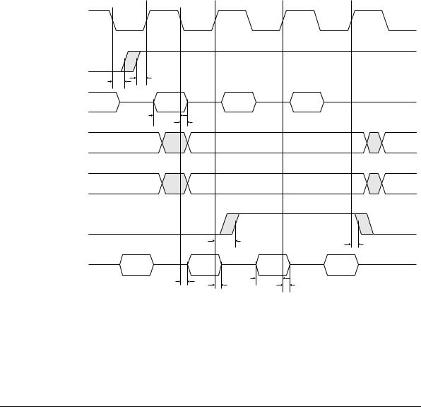
The timing parameters for an ASB decoder with DECODE cycles are shown in Figure 4-40. The parameters for a decoder without DECODE cycles are shown in Figure 4-41. The main difference between the two diagrams is that when DECODE cycles are not inserted then the timing of the DSEL signal becomes dependent on the address and control signal timing.
BCLK |
|
|
|
|
BnRES |
|
|
|
|
|
Tisnres |
|
|
|
|
Tihnres |
|
|
|
BTRAN[1:0] |
N-TRAN |
|
|
|
|
Tistr |
|
|
|
|
|
Tihtr |
|
|
BA[31:0] |
|
|
Address |
|
BWRITE |
|
|
Control |
|
BPROT[1:0] |
|
|
|
|
|
|
|
|
|
DSEL |
|
|
|
|
|
|
Tovdsel |
Tohdsel |
|
|
|
|
|
|
BWAIT |
|
Decoder |
Slave |
|
BERROR |
|
|
||
|
response |
response |
|
|
BLAST |
|
|
||
|
Tisresp |
|
|
|
|
Tovresp |
|
|
|
|
Tohresp |
|
Tihresp |
|
|
|
|
Figure 4-40 ASB decoder with decode cycles
4-68 |
© Copyright ARM Limited 1999. All rights reserved. |
ARM IHI 0011A |
AMBA ASB
BCLK |
|
BnRES |
|
|
Tisnres |
|
Tihnres |
BTRAN[1:0] |
N-TRAN |
|
Tistr |
Tihtr
BA[31:0] |
Address |
|
|
Ttrdsel |
|
|
Tadsel |
|
BWRITE |
Control |
|
BPROT [1:0] |
||
|
||
|
Tctldsel |
|
DSEL |
|
|
|
Tohdsel |
|
BWAIT |
Decoder |
|
BERROR |
||
response |
||
BLAST |
||
Tisresp |
||
|
||
|
Tihresp |
Figure 4-41 ASB decoder without decode cycles
4.12.4Timing parameters
The timing parameters related to an ASB decoder are given in the following tables:
•Table 4-11 is for input signals
•Table 4-12 is for output signals
•Table 4-13 is for combinatorially generated outputs.
ARM IHI 0011A |
© Copyright ARM Limited 1999. All rights reserved. |
4-69 |
AMBA ASB
|
|
Table 4-11 ASB decoder input parameters |
|
|
|
|
Parameter |
Description |
|
|
|
|
Tclkl |
BCLK LOW time |
|
Tclkh |
BCLK HIGH time |
|
Tisnres |
BnRES de-asserted setup to rising BCLK |
|
Tihnres |
BnRES de-asserted hold after falling BCLK |
|
Tistr |
BTRAN setup to falling BCLK |
|
Tihtr |
BTRAN hold after falling BCLK |
|
Tisresp |
BWAIT, BERROR and BLAST setup to rising BCLK |
|
Tihresp |
BWAIT, BERROR and BLAST hold after rising BCLK |
|
|
Table 4-12 ASB decoder output parameters |
|
|
|
|
Parameter |
Description |
|
|
|
|
Tovresp |
BWAIT, BERROR and BLAST valid after falling BCLK |
|
Tohresp |
BWAIT, BERROR and BLAST hold after rising BCLK |
|
Tovdsel |
DSEL valid after rising BCLK |
|
Tohdsel |
DSEL hold after rising BCLK |
|
|
Table 4-13 ASB decoder combinatorial parameters |
|
|
|
|
Parameter |
Description |
|
|
|
|
Ttrdsel |
Delay from valid BTRAN to valid DSEL |
|
Tadsel |
Delay from valid BA to valid DSEL |
|
Tctldsel |
Delay from valid BWRITE and BPROT[1:0] to valid DSEL |
|
|
|
4-70 |
© Copyright ARM Limited 1999. All rights reserved. |
ARM IHI 0011A |