

ivchenko_bookreg
.pdf4 Intraband Optical Spectroscopy of
Nanostructures
The light shines in the darkness,
but the darkness has not overcome it.
John 1: 5
The physics of intersubband transitions in QWs and SLs has attracted increased attention in recent decades, mainly due to the promise of applications in the midand far-infrared regions (2–20 µm) such as detection, modulation, harmonic generation, emission, quantum cascade lasers and photogalvanics.
4.1 Intersubband Optical Transitions. Simple Band
Structure
In bulk semiconductor with a simple band structure direct intraband optical transitions are forbidden by the momentum and energy conservation laws
k = k + q , 2k 2 = 2k2 + ω 2m 2m
because they cannot be satisfied simultaneously. Here k, k are the electron wave vectors in the initial and final states, and q, ω are the light wave vector and frequency. The intraband absorption can only occur by absorption of a photon and simultaneous scattering by “third particle”, e.g., a phonon, another free carrier or a static defect. This process called an indirect optical transition is described by second-order matrix elements involving virtual intermediate states.
Quantum-confinement e ects transform the free-carrier energy spectrum into a series of subbands in QWs or minibands in SLs. As a result we find here an additional mechanism of intraband absorption associated with direct optical transitions of free carriers between the subbands or minibands. Choosing the well and barrier compositional materials one can vary the well dimensions, its height and width, and tune the resonance frequency of intersubband optical transitions to a given value. This opens a clear way for using MQWs and other nanostructures as novel devices and systems in infrared technologies.
4.1.1 Intersubband Light Absorption in a Quantum Well
The transition rate from the electron states i to f is given by Fermi’s golden rule. We consider here the direct optical transitions e1 → e2 between the

172 4 Intraband Optical Spectroscopy of Nanostructures
lowest and first excited subbands in a QW, the transitions eν → eν with arbitrary ν and ν are treated in a similar way. By using equations analogous to (2.142, 2.147) one can present the total transition rate We2,e1 per unit area in the form
We2,e1 |
|
|
|
|
|
|
|
|
|
(4.1) |
|
= |
4π2e2I |
|
ve2s ,e1s(k) 2 |
(fe1sk |
− |
fe2s k)δ(Ee2s k |
− |
|
− |
ω) . |
|
ω2cnω S |
e |
Ee1sk |
|||||||||
|
| · |
| |
|
|
|
|
|
||||
|
|
ss k |
|
|
|
|
|
|
|
|
|
Here I is the light intensity, see (2.141), s, s |
are the spin indices, feνsk is |
||||||||||
the electron distribution function, veν s ,eνs(k) is the matrix element of the velocity operator and S is the sample area.
In a heterostructure consisting of semiconductor layers with a simple con-
duction band, isotropic and parabolic, one has |
|
|||
where veν s ,eνs(k) = δs s k · e ν |m−1(z)|ν + ez ν |vˆz |ν , |
(4.2) |
|||
vˆz = −i 2 |
m(z) ∂z |
+ ∂z m(z) . |
|
|
|
|
1 ∂ |
∂ 1 |
|
For a rectangular QW, in the limit of infinitely high barriers, equation (4.2) simplifies to
e · veν s ,eνs(k) = δs s mA ! k · e |
δν ν + kz |
|
ez " , |
(4.3) |
||||
|
|
|
|
(ν |
ν) |
|
|
|
where |
|
|
|
ν ν |
|
|
|
|
2 |
!1 − (−1)ν +ν " |
|
|
|
||||
kz(ν ν) = i |
|
ν 2 − ν2 . |
|
|
(4.4) |
|||
a |
|
|
||||||
The direct intersubband transitions are allowed in the e |
z polarization |
|||||||
between the subbands of opposite parity. The selection rules, expressed by (4.3), hold for finite barriers as well, provided the e ective masses mA and mB in the well and barrier materials coincide. However, the expression for kz(ν ν) becomes more complicated. If the masses mA, mB are di erent, the matrix elements ν |m−1(z)|ν are nonzero not only for ν = ν but also for ν and ν of the same parity. However the probability of the latter transitions is very small and other corrections to kz(ν ν) including those connected with the band nonparabolicity can play a role.
For a single QW structure the conventional concept of the absorption coe cient, K, is meaningless in the strict sense. Instead one can introduce the absorbance η21, or the fraction of the energy flux absorbed in the QW due to the transitions between the subbands e1 and e2. It can also be defined
as, see (3.27),
η21 = 1 − |r21|2 − |t21|2 ,
4.1 Intersubband Optical Transitions. Simple Band Structure |
173 |
where r21, t21 are the related reflection and transmission coe cients. The absorbance is connected with We2,e1 by
η21I
We2,e1 = (4.5)
ω
and, therefore, the electromagnetic energy absorbed in a unit area of the QW equals to
ωWe2,e1 = η21I .
For the intersubband transitions the reflectivity |r21|2 is negligibly small as compared with η21 and, conditionally, one can define an e ective absorption coe cient KSQW for a single QW by
η21 = 1 − exp (−KSQW a) ≈ KSQW a .
However one should be careful not to overestimate the meaning of KSQW . On the other hand, in short-period MQW structures one can use the approximation of an e ective uniform medium (Sect. 3.1.3) and the e ective absorption coe cient is well defined by
KMQW = ηd21 ,
where d is the period.
Substituting (4.3, 4.4) into (4.1) and integrating over k we obtain
η21 = |
512 e2 |
(N1 |
− N2) |ez |2 δ(E20 − E10 − ω) , |
27 cmAnω |
(4.6)
(4.7)
where Nν is the 2D density of electrons in the ν-th subband; in the following we assume that the 2D equilibrium electrons occupy only the lowest subband ν = 1. The δ-function in (4.7) is k-independent because we assume the same dispersion parabolas in the subbands e1 and e2. The relaxation of electrons results in a homogeneous spectral width, Γ21, of the e2-e1 resonant transition, namely
η21 = |
512 e2 |
(N1 |
− N2) |ez |2 |
1 |
Γ21 |
. (4.8) |
||
27 |
|
cmAnω |
π |
(E20 − E10 − ω)2 + ( Γ21)2 |
||||
Allowance for nonparabolicity of the electron dispersion in the bulk compositional materials, linear-k spin-dependent terms and other e ects removing the equidistance between Ee2s k and Ee1sk lead to an additional broadening of the peak in the intersubband absorption spectrum.
To interpret (4.8) let us replace the system of 2D electron gas by a system of 3D classical electrons confined within a narrow slab of the e ective thickness ae and characterized by the sheet density N1 and conductivity in a unit area given by

174 4 Intraband Optical Spectroscopy of Nanostructures
σzz (ω) = |
N1e2f21 |
−iω |
, |
(4.9) |
|
mAae ω212 − ω2 − 2iωΓ21 |
|||||
|
|
|
|||
where ω21 = E21 and f21 is the so-called oscillator strength. This equation can be derived by solving the equation of motion
d2z |
|
dz |
|
e |
||
|
+ 2Γ21 |
|
+ ω212 |
z = |
|
f21E(t) |
dt2 |
|
|
||||
|
dt |
|
mA |
|||
for a classical oscillator excited by a monochromatic electric field
E(t) = E0 exp (−iωt) + c.c.
The solution is z(t) = z0 exp (−iωt) + c.c. with the amplitude
e f21E0
z0 = mA ω212 − ω2 − 2iωΓ21 .
One can check that the amplitude of the induced current jz = eN3Ddz/dt with N3D = N1/ae can be written as σzz E0 with the conductivity given exactly by (4.9). For weakly-damped oscillators, Γ21 ω21, the denominator can be approximated near the resonance by 2ω21(ω21 − ω − iΓ21).
Equalizing the energy losses η21I to 2ae Re{σzz }|E0|2 we obtain
Re{σzz } = 4cnπaω η21 .
By comparing this equation with the expressions (4.9) for the conductivity and (4.8) for the absorbance we find that the e ective slab model describes the behavior of a 2D electron gas confined in a QW if one takes the dimensionless oscillator strength equal to
256
f21 = 27π2 ≈ 0.96 .
Clearly, the best way to study the subband structure is to observe intersubband optical transitions in the absorption or scattering spectra (the latter will be discussed in Chap. 6). One has however to bear in mind that there are additional e ects which shift the resonance energy from the corresponding subband separation calculated in the single-particle approximation. One of them is called the depolarization e ect. It can be readily understood in the slab model. Actually, the external electric field Eext,z di ers from the field Ez inside the slab. If we introduce the local dielectric function
4πi
æzz (ω) = æb + ω σzz (ω)
with σzz given by (4.9) we can write the relation
æbEext,z = æzz (ω)Ez

4.1 Intersubband Optical Transitions. Simple Band Structure |
175 |
which is nothing more than the boundary condition for the normal component of the electric displacement vector. Therefore the equation jz = σzz Ez can be rewritten in terms of the external field as jz = σ˜zz Eext,z with the renormalized conductivity [4.1]
σ˜zz = |
æb |
σzz = |
N1e2f21 |
−iω |
, |
(4.10) |
|
æzz |
mAae ω˜212 − ω2 − 2iωΓ21 |
||||||
|
|
|
|
||||
where the renormalized resonance frequency is given by
ω˜212 = ω212 + ω212 ,pl
and the intersubband plasmon frequency by
ω2 |
= |
4πN1e2f21 |
. |
(4.11) |
|
|
æbmAae |
||||
21,pl |
|
|
|
|
|
|
|
|
|
|
|
Taking into account the depolarization e ect the rate of energy losses is given by 2ae Re{σ˜zz }|Eext,z |2 instead of 2ae Re{σzz }|Ez |2 and exhibits its maximum at the frequency ω˜21.
Physically, the depolarization e ect arises because each electron feels a field which is di erent from the external field by the mean Hartree field of other electrons perturbed by the external field. In fact, the Hartree approximation is valid when the average kinetic energy of electrons is much larger than the average interaction energy. Otherwise this approximation overestimates the Coulomb repulsive force of other electrons, many-body e ects such as exchange and correlation can play an important role and reduce the renormalization of the resonance energy ω21 [4.1]. A more rigorous treatment of the linear response of an n-doped QW to an external electric field, Eext,z , leads the conductivity σ˜zz (ω) given in the form of (4.10) with f21 = (2mAω21/ ) 2|z|1 2 and
ω˜212 = ω212 (1 + α21 − β21) . |
(4.12) |
The coe cients α21, β21 describe the depolarization and exchange-correlation e ects, respectively. The former is defined by
|
|
α21 = |
8πN1e2L21 |
, |
(4.13) |
||
|
|
ω21æb |
|||||
|
|
|
|
|
|||
where |
∞ |
|
|
|
z |
|
|
|
|
z |
|
|
|
||
L21 = |
|
dz ϕ2(z) ϕ1(z) |
dz |
|
dz ϕ2(z ) ϕ1(z ) |
|
|
|
−∞ |
|
−∞ |
|
−∞ |
|
|
and ϕν (z) is the electron envelope in the subband ν. Therefore, the intersubband plasmon frequency can be written as

176 4 Intraband Optical Spectroscopy of Nanostructures
ω212 ,pl ≡ ω212 α21 = |
8πN1e2L21 |
ω21 |
, |
(4.14) |
||||
æb |
|
|||||||
which coincides with (4.11) if we set |
|
|
|
|
|
|||
|
f21 |
= |
2L21ω21mA |
. |
|
|
|
|
|
ae |
|
|
|
|
|
||
An explicit equation for the coe cient β21 can be found in [4.1]. Note that the corresponding term includes the exciton-like correction which appears due to the interaction between the excited electrons in the e2 subband and the empty state, or holes, in the e1 subband.
In an ideal QW, the energy spacing E21 = E20 − E10 exhibits no random variations in the interface plane and the spectral width of the absorption can be estimated by
δ21 max |
2 ¯2 |
|
m , Γ21 , |βν |k¯ |
, |
(4.15) |
2m |
|
||||
|
k |
|
δm |
|
|
where δm is the di erence of the electron e ective masses in the subbands e1 and e2 due to the nonparabolicity, βν is the coe cient describing linear-k
¯
terms in the electron e ective Hamiltonian, and k is an average value of the wave vector in the equilibrium 2D electron gas occupying states in the lower subband e1. The latter has an order of magnitude of the Fermi wave vector in
case of the degenerate statistics and the thermal wave vector 2m1kB T / 2 for the Maxwell distribution. As a rule, in available QW structures the width, ∆21, of inhomogeneous broadening of the gap E21 exceeds the width δ21 of absorption spectrum in an ideal QW. The inhomogeneous broadening can be taken into consideration by introducing the distribution function, F (E21), of the gap E21 and replacing (4.6, 4.7) by
K |
|
= |
256π2e2 2(N1 − N2) |
F ( ω) e |
z | |
2 . |
(4.16) |
|
9nω ca2mA2 ωd |
||||||
|
MQW |
|
| |
|
|
The shape of the function F (E21) can be found from a comparison with experiment [4.2] or calculated by using a particular model of the interface roughness [4.3].
In the above description of an intersubband resonance in a QW the confinement dictates that the electric vector of the light wave must have a nonzero component ez along the growth direction in order to excite the e2-e1 intersubband transition. This one-band picture is modified in a multiband description of the band structure. The main result is that through k ·p band coupling, notably mixing of the conduction states with the heavy, light and spin-orbit-split hole states, all four transitions e1, ±1/2 → e2, ±1/2 are allowed, some of them in the polarization e z plane and others in the polarization e z plane. For a QW of the D2d point symmetry, the e1 and e2
4.1 Intersubband Optical Transitions. Simple Band Structure |
177 |
subband states at k = 0 transform according to the spinor representations Γ6 and Γ7. In the D2d point group, the direct product
Γ6 × Γ7 = Γ1 + Γ2 + Γ5 |
(4.17) |
with excitations of the symmetry Γ2 and Γ5 (or B and E in other notations) being optically active, respectively, in the polarization e z and e z. Therefore, the intersubband matrix elements of the velocity operator at k = 0 are, in general, characterized by two linearly-independent coe cients. One may show that they can be presented in the form
|| · |
|
|
|| |
|
−V (ex + iey ) |
V ez |
|
|
e |
ve2s |
,e1s |
|
= |
V ez |
V (ex − iey ) |
. |
(4.18) |
The coe cients V and V describe the spin-conserving (s = s) and spin-flip (s − s = ±1) transitions, respectively. By using the Kane model we can present the electron wave function in the subband ν at k = 0 as
|
|
|
|
√3m0 |
|
Eg + Eν0 |
|
|
− Eg + ∆ + Eν0 |
|
|||||||||||||||||
ψeν,1/2 = |
uΓ6,1/2 + |
p |
√2uΓ |
,1/2 |
|
|
|
uΓ |
,1/2 |
ˆ |
ϕν (z) , |
||||||||||||||||
|
|
|
cv |
|
8 |
|
|
|
|
|
|
|
7 |
|
|
|
|||||||||||
|
|
|
|
|
|
|
|
|
|
|
|
|
|
|
|
|
|
|
|
kz |
|||||||
|
|
|
|
|
|
|
|
|
|
|
|
|
|
|
|
|
|
|
|
||||||||
|
|
|
|
|
|
|
|
|
|
|
|
|
|
|
|
|
|
|
|
||||||||
− |
|
|
− |
|
√3m0 |
E |
g + Eν0 |
|
|
Eg + ∆ + Eν0 |
|
||||||||||||||||
|
1/2 = |
|
|
1/2 + |
p |
|
|
√2 |
uΓ |
|
, |
− |
1/2 |
+ |
uΓ |
, |
− |
1/2 |
ˆ |
ϕν (z) , |
|||||||
|
uΓ6, |
|
|
|
|
|
cv |
|
8 |
|
|
|
|
|
7 |
|
|
||||||||||
ψeν, |
|
|
|
|
|
|
|
|
|
|
|
|
|
|
|
|
|
|
|
|
|
kz |
|||||
|
|
|
|
|
|
|
|
|
|
|
|
|
|
|
|
|
|
|
|
|
|||||||
|
|
|
|
|
|
|
|
|
|
|
|
|
|
|
|
|
|
|
|
|
|||||||
where the admixture of the valence-band states is included. An important point is that the energy denominators are dependent on the quantumconfinement energy which leads to a nonzero value of V . Taking into account that m m0 one has in the non-vanishing approximation [4.4]
V ≡ v21 = |
|
(4.19) |
m kz(21) , |
V ≡ v21Λ , Λ = |
E21∆(2Eg + ∆) |
|
. |
2Eg (Eg + ∆)(3Eg + |
2∆) |
Therefore, taking into account o -diagonal components in (4.18) we can rewrite (4.16) in a more general form
KMQW(e) = Kz |ez |2 + K (|ex|2 + |ey |2) , |
(4.20) |
||||
where |
256π2e2 2(N1 − N2) |
|
|
|
|
Kz = |
F ( ω) , K |
|
= Λ2Kz |
(4.21) |
|
|
9nω ca2mA2 ωd |
|
|
||
and, for simplicity, the depolarization and exchange-correlation e ects are ignored.
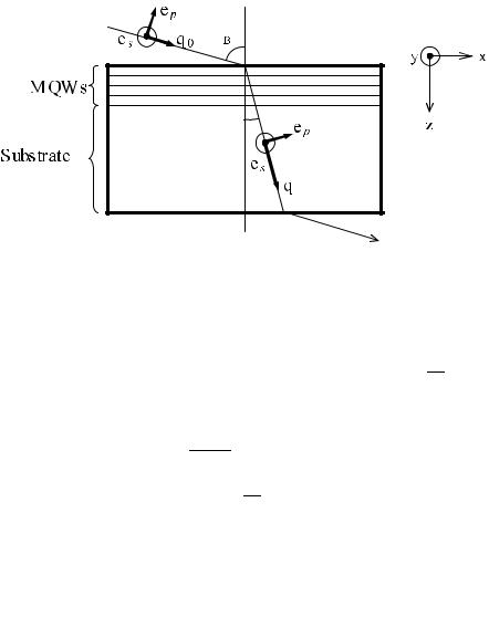
Figure 4.1 illustrates the geometry of experiment on light transmission through a MQW structure. Since Λ2 1 and, in the e z polarization, the
178 4 Intraband Optical Spectroscopy of Nanostructures
θ
θ
Fig. 4.1. Schematic representation of light reflection from a MQW structure under oblique incidence at Brewster’s angle θBr.
intersubband transitions are very weak, the oblique incidence of p-polarized light is used [4.5]. To exclude the losses associated with reflection from the top and bottom faces of the sample, one may conveniently shine the infrared light under the Brewster angle, θBr, satisfying the condition tan θBr = √æb, where æb is the dielectric constant of the barrier. Neglecting the light absorption in the barrier, we obtain for the transmission coe cient
− ln T = |
Kz N d |
(sin2 θ + Λ2 cos2 θ) , |
(4.22) |
cos θ |
where N is the number of wells in the structure, and θ is the refraction angle related with the Brewster angle by √æb sin θ = sin θBr. Taking into account that in the Brewster geometry
cos θ = |
|
æb + 1 |
, |
|
cos θ = |
|
æb(æb + 1) |
, |
|||
|
|
æb |
|
sin2 |
θ |
1 |
|
||||
one has |
|
|
|
|
|
|
|
||||
− ln T = Kz N d |
|
1 + Λ2æb |
(4.23) |
||||||||
|
|
. |
|||||||||
|
æb(æb + 1) |
||||||||||
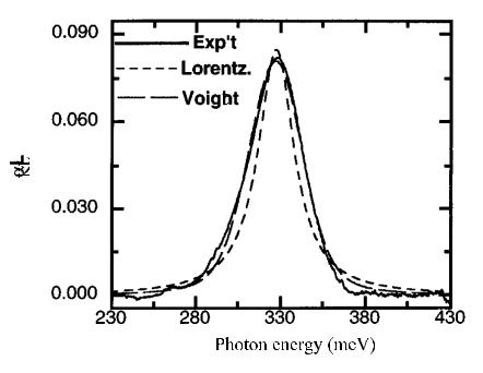
Figure 4.2 shows an experimental |
intersubband absorption spectrum of the |
||||||||||
|
|
|
˚ |
˚ |
|||||||
sample containing a MQW structure with 40-A In0.45Ga0.55As wells and 80-A
Al0.45Ga0.55As barriers. The absorption was measured by a Fourier-transform infrared spectrometer with p-polarized light at Brewster’s angle. The dashed and broken lines in Fig. 4.2 are the best fits with the Lorentzian and the Voigt line shapes, respectively. Note that the Voigt profile is a convolution of a Gaussian representing an inhomogeneous broadening with a Lorentzian representing a homogeneous broadening.
|
4.1 Intersubband Optical Transitions. Simple Band Structure |
179 |
||
|
|
|
|
|
|
|
|
|
|
|
|
|
|
|
|
|
|
|
|
Fig. 4.2. Experimental (Exp’t) absorption spectrum of InGaAs/AlGaAs MQW structure using p-polarized light at Brewster’s angle, along with the best Lorentzian (Lorentz.) and Voigt line shapes. From [4.2].
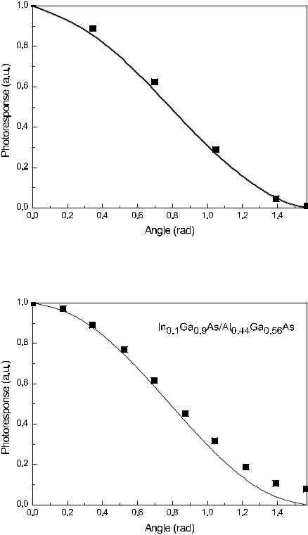
Using QW infrared detectors with either GaAs or InGaAs QWs, Liu et al. [4.6] experimentally investigated the accuracy of the polarization selection rule for the conduction band intersubband transitions. Figure 4.3 plots the normalized photosignal taken at the Brewster angle incidence at the wavelength 8.1 µm and 4.6 µm from GaAs/Al0.26Ga0.74As and In0.1Ga0.9As/Al0.44Ga0.56As QW detectors, respectively. In the figure, squares represent the photoresponse signal as a function of the angle between the plane of incidence and the plane of polarization. For quantitative comparisons, the reflection (69%) of the s-polarized light at the sample/vacuum interface must be taken into account. The experiments imply that the s-to-p ratio does not exceed 0.22% in the GaAs QWs and 3% in the InGaAs QWs in agreement with a small value of the parameter Λ.
To increase the radiation energy absorbed in the sample containing MQWs, the side faces of the sample can be prepared in the so-called waveguide geometry by cleaving or polishing two parallel side faces at some angle. In this case the light is directed through the faces, as illustrated in Fig. 4.4, thus exciting the waveguide modes. Figure 4.5 shows the resonance behavior of absorption measured in n-GaAs/AlGaAs MQWs by making use of trans-
180 4 Intraband Optical Spectroscopy of Nanostructures
Fig. 4.3. Measured photoresponse signal vs. polarization azimuthal angle ϕ for (top panel) a GaAs/AlGaAs and (bottom panel) an InGaAs/AlGaAs QW (T = 80 K). The ideal cos2 ϕ relation is shown by the solid line. The size of the symbol represents the measurement error bar. From [4.6].