

Abstract_15 молодёжная школа
.pdfРис. 13. РЭМ-изображение массива микроострий на поверхности образца 3.03 при разных увеличениях. Форма острий – пирамидальная-полусферическая.
Средняя плотность острий по образцу – 3·106 см-2.
Сформированные в результате обработки поверхности микроострия представляют собой монокристаллический карбид кремния. Результаты рентгеноспектрального микроанализа состава отдельных острий, проведенные на спектрометре с энергетической дисперсией прибора Helios Nanolab в режиме вычитания фона в каждой точке скана представлены на рис.14.
20
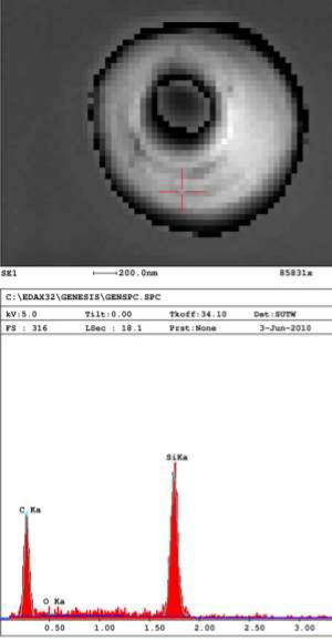
Рис. 14. Область сканирования и рентгеновский спектр отдельного микроострия. Соотношение интенсивностей линий Si-Kα и C-Kα соответствует составу, близкому к стехиометрическому
Чрезвычайно важной для создания АВМП представляется возможность формирования на поверхности пластин SiC топологически упорядоченных массивов микроострий с необходимой плотностью и формой отдельного острия. На рис. 15 приведены РЭМ-изображения одиночного микроэмиттера, фрагмента массива и топологически упорядоченного массива микроэмиттеров на 6H-SiC .
21
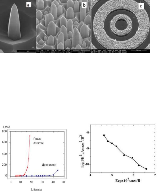
Рис. 15. РЭМ-изображения одиночного микроэмиттера с наноразмерной вершиной острия (а), фрагмента массива (b) и
топологически упорядоченного массива микроэмиттеров (с) Исследования автоэмиссионных свойств сформированных структур проводились по диодной схеме в сверхвысоком вакууме P = 10-9 мм. рт. ст. Было установлено, что эмиссионные свойства карбидокремниевых острийных катодов слабо зависят от уровня вакуума в пределах (10-6 – 10-9) мм. рт. ст., но существенным образом изменяются после проведения вакуумной электрополевой очистки поверхности. Типичные ВАХ до и после такой очистки приведены на рис. 16, a, на рис. 16, б – ВАХ одной из эмиссионных структур в координатах Фаулера –Нордгейма.
а) |
б) |
Рис. 16. ВАХ автоэмиссионной структуры до и после вакуумной электрополевой очистки (а) и ВАХ в координатах Фаулера – Нордгейма (б)
На структурах с оптимизированным габитусом микроострий 4H-SiC получены плотности тока порядка 102 А/см2, что обеспечивает возможность создания АВМП различного функционального назначения.
22
Заключение
Приведенные выше результаты показывают, что основой для создания новых компонентов электроники с экстремальными энерговременными параметрами, могут быть широкозонные политипы карбида кремния. При этом обеспечиваются параметры и характеристики (dU/dt)max для 4H-SiC ДДРВ, плотности тока полевой эмиссии для АВМП, удельные коммутируемые мощности, рабочие температуры, уровень стойкости к радиационным воздействиям, недостижимые на традиционных материалах микроэлектроники – кремнии и арсениде галлия.
Библиографический список
1.Грехов И.В., Ефанов В.М., Кардо-Сысоев А.Ф. Формирование высоковольтных наносекундных перепадов напряжения на полупроводниковых диодах.
Письма в ЖТФ, 1983, Т. 9. Вып. 7. С. 435.
2.Корольков В.И., Рожков А.В., Петропавловская Л.А. Высоковольтные арсенидгаллиевые диоды с субнаносекундными временами восстановления блокирующего напряжения. Письма в ЖТФ, 2001, Т. 27. Вып. 17. С. 46 - 50.
3.Грехов И.В., Иванов П.А., Константинов А.О. О возможности создания диода со сверхрезким восстановлением запирающих свойств на основе карбида кремния. Письма в ЖТФ, 2002, Т. 28. Вып. 13. С. 24 - 29.
4.A.F. Kardo-Sysoev, V.I. Brylevsky, Y.S. Lelikov, I.A. Smirnova, S.V. Zazulin Generation and Radiation of Powerful Nanosecond and Subnanosecond Pulses at High Pulse Repetition Rate for UWB System. Inter. Conf. Euroem 2000, Edinburg, Scotland, UK, 30 May - 2 June, 2000.
5.B.R. Gossick. On the transient Behavior of Semiconductor Rectifiers. J. Appl. Phys., 27, 905 (1956).
Исследования проводились в рамках Программы стратегического развития университета (СПбГЭТУ «ЛЭТИ») «Развитие междисциплинарных исследований и инструментально-технологической базы как основа непрерывного инженерного образования по приоритетным направлениям российской экономики» на
2012-2016 годы.
23
ПЛЕНАРНЫЕ ДОКЛАДЫ
DEVELOPMENT SEMICONDUCTOR SiC FROM 1893 TO PRESENT
Y. M. Tairov
St. Petersburg Electrotechnical University,
e-mail: SiCLab-Tairov@yandex.ru
In year 1893. The starting point in history of silicon carbide.
Just then a great American researcher Acheson, Edward Goodrich invented process for industrial purposes SiC effective abrasive material.
In Acheson's furnaces can be found inclusions of single crystals hexagonal cut up to 25-30mm.
These crystals were the subject of research for several decades until the midfifties of last century.
In year 1907. An American researcher H. J. Round observed the phenomenon of luminescence from silicized carbon (SiC) detector contact.
In 1926. The outstanding Russian researcher O. V. Losev received the first patent of device with an electroluminescent light source based on Acheson SiC crystal.
The first half of the 20th century. Crystallographic studies of Acheson crystals, made in different laboratories around the world, have made it possible to identify dozens of different polytypies of silicon carbide. List of research can be extended.
In 1955. A turning point in the semiconductor studies of silicon carbide. German scientist Lely invented sublimation process for growing crystals, spurring a wave SiC research. Electrical properties of semiconductor silicon carbide, the characteristics of electronic and optoelectronic devices based on silicon carbide, etc., were studied in many laboratories. The number of publications increased greatly.
In 1959. C. E. Ryan, Air Force Cambridge Research Labs with colleagues organized Fist International Conference on Silicon Carbide Boston, Massachusetts, USA. At the conference, reports were made that showed the unique properties of SiC as a material for the next generation of electronics. As a result, the number of research centers studying silicon carbide, grown throughout the world. Local conferences, seminars, round tables were held in many countries. Only in the Soviet Union from 1961 to 1970 there were five conferences.
In 1964. In USSR was founded first industrial production monocrystalline SiC (Lely method) in Podolsk Chemical-Metallurgical Plant (near Moscow).
In 1968. Second International Conference on Silicon Carbide, University Park, Pennsylvania. The conference was organized with the active participation of C. E. Rayn and W. J. Choyke.
24
In 1973. Third International Conference on silicon carbide, Miami Beach, USA. However, by this time the governments and companies have dramatically reduced funding for research on silicon carbide. The reason was the lack of industrial method of growing bulk crystals of silicon carbide, as well as great advances in the technology of III-V. The number of scientific publications SiC drastically reduced.
In 1976. The situation began to change. Tairov and Tsvetkov created modified Lely process (LETImethod).
In 1982. LETI - method is implemented in the Podolsk Chemical-Metallurgical Plant.
In 1987. The real quantum leap in industrial development of silicon carbide. Creating Cree Research Inc. in North Caroline, USA.
In 1991. SiC wares became commercially from Cree. After that, the opportunity to design and build various devices based on silicon carbide has become a reality. There are currently designed and manufactured devices such as bipolar diodes, Schottky diodes, unipolar transistors (MOSFET, JFET), bipolar transistors (BJT, GTO), RF transistors (MESFET), LED, different sensors (temperature, pressure, ultra violet radiation and so on), SiC MEMS, Autoemission nanosized cathodes and many others.
РОСТ И ИССЛЕДОВАНИЕ ЭПИТАКСИАЛЬНЫХ СЛОЁВ 3C-SiC, ВЫРАЩЕННЫХ НА ПОДЛОЖКАХ ГЕКСАГОНАЛЬНОГО SiC
A.A. Лебедев Физико-технический институт им. А.Ф. Иоффе РАН
Известно, что кубический карбид кремния (3С-SiC) является одним из наиболее интересных политипов SiC. 3С-SiC обладает наибольшей среди политипов SiC и не зависящей от кристаллографического направления подвижностью электронов (1200 см2/В·с). Остальные параметры 3С (критическое электрическое поле, максимальные рабочие температуры, скорость насыщения электронов, теплопроводность) не значительно отличаются от параметров гексагональных политипов. Таким образом, 3С-SiC является весьма перспективным материалом для создания различных типов полупроводниковых приборов. Однако до настоящего времени отсутствуют монокристаллические подложки 3С-SiC , а электрические параметры изучены достаточно слабо.
Эпитаксиальные слои 3C-SiC толщиной до 100 мкм были получены методом сублимационной эпитаксии на гексагональных (6H-SiC) подложках. Максимальные скорости роста достигали 200 мкм/час. Специально не легированные слои имели n – тип проводимости ( Nd-Na ~ 1017 -1018 см-3). В спектре фотолюми-
25

несценции преобладала донорно-акцепторная рекомбинация (Al-N) hνMAX ~ 2.12 эВ. Представлен подробный анализ спектра фотолюминесценции, полученный при 6 К. Сделан вывод, что данные эпитаксиальные слои могут быть использованы как подложки для создания приборов на основе 3C-SiC.
Проведено исследование низкотемпературной проводимости и магнетосопротивления полученных пленок в зависимости от уровня легирования и структурного совершенства. Обнаружено, что при концентрациях Nd – Na в слое n – 3C-SiC 3·1017 см-3 происходит переход металл – диэлектрик.
С использованием источника роста, содержащего Al, были получены сильнолегированные (Na – Nd ~ 2 – 3·1018 см-3) эпитаксиальные слои p-3C-SiC. Проведенные электрофизические исследования показали, что энергия активации акцепторной примеси в этих слоях существенно ниже, чем известные литературные данные, полученные из исследования спектров ФЛ n-3C-SiC <Al>. Повидимому, это связано с тем, что при концентрациях Al 1018 см-3, происходит уменьшение энергии ионизации алюминия (либо образования другого типа акцепторных центров). Подобная зависимость энергии ионизации алюминия от его концентрации наблюдалась ранее для гексагональных политипов SiC.
На основе полученной эпитаксиальной p-n структуры были сформированы диоды и проведены исследования их параметров методами I-V и C-V характеристик, электролюминесценции. Характеристики исследовавшихся диодов близки характеристикам диодов на основе объемного 3С-SiC. Сделан вывод о применимости метода сублимационной эпитаксии для получения 3С-SiC p-n структур на основе подложек других политипов карбида кремния.
Был обнаружен переходный слой между подложкой 6H-SiC и 3C-пленкой. Он представляет собой смесь 3C и 6H политипов, имеет переменную толщину. Наличие переходного слоя, по-видимому, мешает проявлению квантоворазмерных эффектов на гетеропереходе 3С-SiC\6H-SiC, и не позволяет создавать приборы типа HEMT транзистора на основе гетерополитипных структур. Следует также отметить, что толщина переходного слоя, также как и общая концентрация дефектов снижалась с увеличением однородности слоя 3С-SiC (с исчезновением включений гексагональной фазы). Таким образом, можно предположить, что исчезновение переходного слоя будет наблюдаться в гетероструктурах 3С-SiC\6H-SiC, где слой кубического политипа будет состоять из одного или нескольких двойников.
26
COMPUTER MODELING OF EPITAXIAL SILICON CARBIDE TRANSFORMA-
TION OF GRAPHENE.
SEMI-EMPIRICAL QUANTUM CHEMISTRY APPROACH
N.I. Alekseyev
Saint-Petersburg Electrotechnical University «LETI», Russia
E-mail: NIAlekseyev@yandex.ru
Semi-Empirical Quantum Chemistry (QC) methods enable the transformation SiCgraphene (Gr) in the course of high temperature epitaxy to be analyzed in details. The advantage of this approach is a possibility to understand the nature of a defective character of epitaxial graphene structures.
As a test for suitability of our approach the variants of reconstruction for Si (0001)- and Carbon (000–1) faces, preceding the Gr synthesis, are researched. It is shown that the simulation reproduces principal experimental results such as a [6√3x6√3]R300 reconstruction for the Si face as well as a specific sequence of smallscale reconstructions for the carbon face.
Reconstruction of the both (0001) and (000–1) faces starts with breaking one of the bonds of the upper layer of SiC. But the weakest link is different for these cases. In the case of the Si face this link is a Si atom with broken bond. This atom is evaporated easily to form the initial breakage of the surface. This easy evaporation tendency remains at further reconstruction steps.
For the C face the role of the weakest link or of an active element is played by the carbon atom, bonding one of the closest carbon atoms.
Easier evaporation of Si atoms within the upper Si face layer creates deformed cells with additional C-C bonding in horizontal layer and still more weakened Si atoms. The evaporation of these atoms favors subsequent horizontal bonding of carbon atoms in the upper SiC layer. Therefore a compact Gr cluster is formed at the place of the upper layer destruction (Fig. 1).
The following tendencies are realized in the growth of such clusters. An uncompensated energy owing to the lattice mismatch between the Gr cluster and underlying SiC layer, is increased. Another uncompensated energy owing to the lattice mismatch between the cluster and upper layer of SiC, surrounding it, is also increased. As a sequence a detachment of the cluster from the breakage of the upper layer of SiC is favorable at some size of the island (Fig. 2). This size is approximately correspondent with one reconstruction cell √3х√3−300.
An averaged distance between the Gr clusters is close to their arrangement at centers of (2√3х2√3)R300 reconstruction lattice. This lattice is commensurable with the experimentally observed 6√3х6√3−300 reconstruction. So, the both of the known
27

typical scales of fore-Gr reconstruction are present in the modeling.
The entropy and Gibbs energy calculation in the course of the destruction of the secondand the third layer of SiC shows: at the temperature that ensures Gr cluster generation from the first layer atoms as a spontaneous process, the proliferation of the clusters at the expense of underlayers occurs as a spontaneous process also; typical temperatures of the process which develops when the SiC surface is evaporated to a noble gas atmosphere or to vacuum, are in a good correspondence with experimental date.
In the case of carbon face a spontaneous breakage of a Si-C bond in the upper layer (000–1) of SiC evolves the bonding of the weakened carbon atom with one of closest carbon atoms. This bonding forms short C-C-C chain approximately in the layer surface. The Si atom evaporation is comparatively less probable; it can develop no sooner than the chain is formed. So the lattice of chains is formed with the superstructure formula 2х2 as related to the initial carbon atom lattice in the (000–1) surface of SiC (Fig. 3).
In the course of a transfer from the 2x2 superstructure of chains to a 3x3 superstructure the nuclei of this superstructure are formed as pairs of Gr cells. A proliferation of these nuclei at the expense of the third layer develops within 3x3 formula also (a structure, optimally correlated with Si-C lattice, is shown in Fig. 4)
Fig. 1. Evaporation of Si atoms out of SiC upper layer forms a compact cluster of Gr cells (shown in bold lines). C- and Siatoms in SiC upper layer are black and white circles subsequently, second layer atoms are grey circles
Fig. 2. Typical Gr cluster (its atoms
are shown in black circles) of Nisl=20 atoms at the moment of its detach-
ment from the breakage border (dotted line)
28
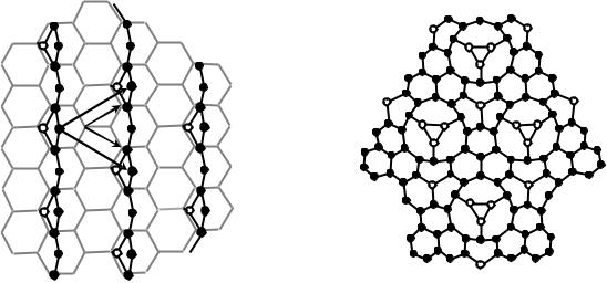
Fig. 3. 2x2 reconstruction lattice (long arrows) as related to initial carbon atom lattice in [000–1] SiC upper layer (short arrows)
Fig. 4. A structure with 3x3 reconstruction formula optimally matched with SiC lattice (less than 1% mismatch)
HIGH TEMPERATURE GRAPHENE PREPARATION AND PROPERTIES
Rositza Yakimova
Department of Physics, Chemistry and Biology, Linköping University, Sweden
E-mail: roy@ifm.liu.se
Graphene grown on SiC does not need transferring to a substrate and can extend over 100 mm in diameter, which is a standard SiC wafer size to date. This material system is considered to be promising for RF transistors, highly sensitive gasand biosensors, spin valves and devices based on the particular quantum effects in graphene. While the former listed applications are still at an exploratory stage, the half integer quantum Hall effect has been used to establish new quantum resistance standard prototype thanks to the availability of large area high quality epitaxial graphene on SiC.
We are fabricating wafer scale epitaxial graphene on SiC substrates by using high temperature sublimation process in an inductively heated furnace of vertical geometry, the latter being an advantage as compared to a horizontal set up because of a better temperature uniformity. An important issue in this type of graphene is that its electronic properties are to a large extent buffer layer mediated. Therefore the effect of the interface along with the surface uniformity and morphological stability of the grown graphene monolayers are of a primary significance.
In this talk we are going to present recent understanding of graphene formation mechanism on different polytypes (6H, 4H and 3C) with the ultimate goal to fabricate large area graphene with controlled number of mono-layers and spatial uniformity. El-
29