


nRF24L01+ Product Specification
Symbol |
Parameters |
Min. |
Max |
|
Units |
Tdc |
Data to SCK Setup |
2 |
|
|
ns |
Tdh |
SCK to Data Hold |
2 |
|
|
ns |
Tcsd |
CSN to Data Valid |
|
75 |
|
ns |
Tcd |
SCK to Data Valid |
|
85 |
|
ns |
Tcl |
SCK Low Time |
40 |
|
|
ns |
Tch |
SCK High Time |
40 |
|
|
ns |
Fsck |
SCK Frequency |
0 |
5 |
|
MHz |
Tr,Tf |
SCK Rise and Fall |
|
100 |
|
ns |
Tcc |
CSN to SCK Setup |
2 |
|
|
ns |
Tcch |
SCK to CSN Hold |
2 |
|
|
ns |
Tcwh |
CSN Inactive time |
50 |
|
|
ns |
Tcdz |
CSN to Output High Z |
|
75 |
|
ns |
|
Table 26. SPI timing parameters (Rpull = 50kΩ, Cload = 50pF) |
|
|||
|
|
|
|
|
|
Symbol |
Parameters |
Min. |
Max |
|
Units |
Tdc |
Data to SCK Setup |
2 |
|
|
ns |
Tdh |
SCK to Data Hold |
2 |
|
|
ns |
Tcsd |
CSN to Data Valid |
|
116 |
|
ns |
Tcd |
SCK to Data Valid |
|
121 |
|
ns |
Tcl |
SCK Low Time |
40 |
|
|
ns |
Tch |
SCK High Time |
40 |
|
|
ns |
Fsck |
SCK Frequency |
0 |
4 |
|
MHz |
Tr,Tf |
SCK Rise and Fall |
|
100 |
|
ns |
Tcc |
CSN to SCK Setup |
2 |
|
|
ns |
Tcch |
SCK to CSN Hold |
2 |
|
|
ns |
Tcwh |
CSN Inactive time |
50 |
|
|
ns |
Tcdz |
CSN to Output High Z |
|
116 |
|
ns |
Table 27. SPI timing parameters (Rpull = 50kΩ, Cload = 100pF)
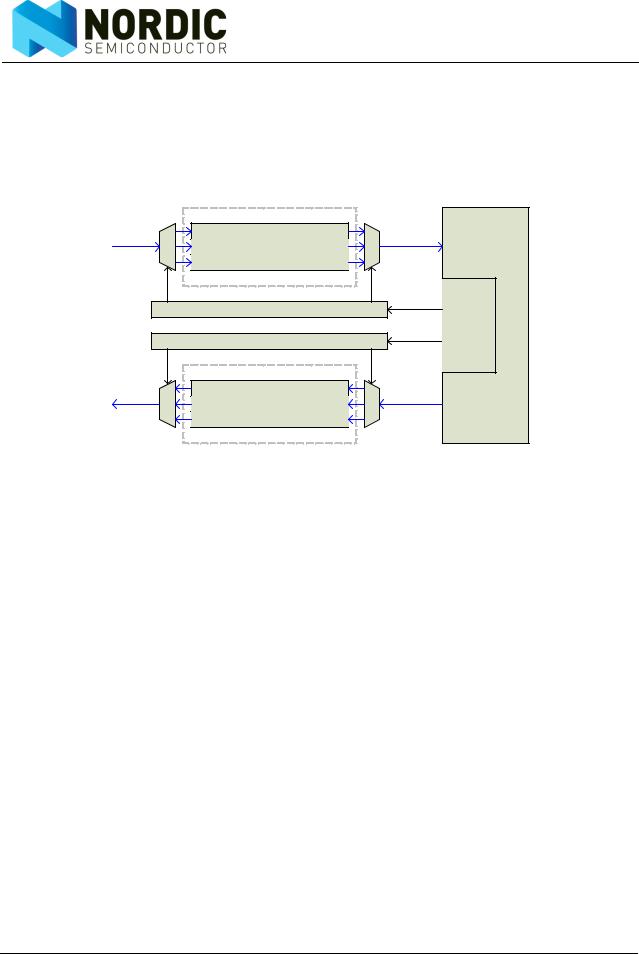
8.4Data FIFO
The data FIFOs store transmitted payloads (TX FIFO) or received payloads that are ready to be clocked out (RX FIFO). The FIFOs are accessible in both PTX mode and PRX mode.
The following FIFOs are present in nRF24L01+:
•TX three level, 32 byte FIFO
•RX three level, 32 byte FIFO
Both FIFOs have a controller and are accessible through the SPI by using dedicated SPI commands. A TX FIFO in PRX can store payloads for ACK packets to three different PTX devices. If the TX FIFO contains more than one payload to a pipe, payloads are handled using the first in - first out principle. The TX FIFO in a PRX is blocked if all pending payloads are addressed to pipes where the link to the PTX is lost. In this case, the MCU can flush the TX FIFO using the FLUSH_TX command.
The RX FIFO in PRX can contain payloads from up to three different PTX devices and a TX FIFO in PTX can have up to three payloads stored.
Revision 1.0 |
Page 55 of 78 |
nRF24L01+ Product Specification
You can write to the TX FIFO using these three commands; W_TX_PAYLOAD and W_TX_PAYLOAD_NO_ACK in PTX mode and W_ACK_PAYLOAD in PRX mode. All three commands provide access to the TX_PLD register (see Table 28. on page 63. for details of this register).
The RX FIFO can be read by the command R_RX_PAYLOAD in PTX and PRX mode. This command provides access to the RX_PLD register.
The payload in TX FIFO in a PTX is not removed if the MAX_RT IRQ is asserted.
|
RX FIFO |
|
|
|
32 byte |
|
|
Data |
32 byte |
Data |
|
32 byte |
|
||
|
|
|
|
|
RX FIFO Controller |
Control |
|
|
SPI |
SPI |
|
|
|
||
|
|
command |
|
|
TX FIFO Controller |
decoder |
|
|
|
||
|
Control |
|
|
|
|
|
|
|
TX FIFO |
|
|
Data |
32 byte |
Data |
|
32 byte |
|
||
|
|
|
|
|
32 byte |
|
|
Figure 30. FIFO (RX and TX) block diagram
You can read if the TX and RX FIFO are full or empty in the FIFO_STATUS register.
8.5Interrupt
The nRF24L01+ has an active low interrupt (IRQ) pin. The IRQ pin is activated when TX_DS IRQ, RX_DR IRQ or MAX_RT IRQ are set high by the state machine in the STATUS register. The IRQ pin resets when MCU writes '1' to the IRQ source bit in the STATUS register. The IRQ mask in the CONFIG register is used to select the IRQ sources that are allowed to assert the IRQ pin. By setting one of the MASK bits high, the corresponding IRQ source is disabled. By default all IRQ sources are enabled.
Note: The 3 bit pipe information in the STATUS register is updated during the IRQ pin high to low transition. The pipe information is unreliable if the STATUS register is read during an IRQ pin high to low transition.
Revision 1.0 |
Page 56 of 78 |