

nRF24L01+
Single Chip 2.4GHz Transceiver
Product Specification v1.0
Key Features |
Applications |
||
• Worldwide 2.4GHz ISM band operation |
• |
Wireless PC Peripherals |
|
• 250kbps, 1Mbps and 2Mbps on air data |
• Mouse, keyboards and remotes |
||
|
rates |
• |
3-in-1 desktop bundles |
• Ultra low power operation |
• Advanced Media center remote controls |
||
• 11.3mA TX at 0dBm output power |
• |
VoIP headsets |
|
• 13.5mA RX at 2Mbps air data rate |
• |
Game controllers |
|
• 900nA in power down |
• Sports watches and sensors |
||
• |
26µA in standby-I |
• RF remote controls for consumer electronics |
|
• On chip voltage regulator |
• Home and commercial automation |
||
• 1.9 to 3.6V supply range |
• Ultra low power sensor networks |
||
• |
Enhanced ShockBurst™ |
• |
Active RFID |
• |
Automatic packet handling |
• |
Asset tracking systems |
• Auto packet transaction handling |
• |
Toys |
|
•6 data pipe MultiCeiver™
•Drop-in compatibility with nRF24L01
•On-air compatible in 250kbps and 1Mbps with nRF2401A, nRF2402, nRF24E1 and nRF24E2
•Low cost BOM
•±60ppm 16MHz crystal
•5V tolerant inputs
•Compact 20-pin 4x4mm QFN package
All rights reserved.
Reproduction in whole or in part is prohibited without the prior written permission of the copyright holder. September 2008

nRF24L01+ Product Specification
Liability disclaimer
Nordic Semiconductor ASA reserves the right to make changes without further notice to the product to improve reliability, function or design. Nordic Semiconductor ASA does not assume any liability arising out of the application or use of any product or circuits described herein.
All application information is advisory and does not form part of the specification.
Limiting values
Stress above one or more of the limiting values may cause permanent damage to the device. These are stress ratings only and operation of the device at these or at any other conditions above those given in the specifications are not implied. Exposure to limiting values for extended periods may affect device reliability.
Life support applications
These products are not designed for use in life support appliances, devices, or systems where malfunction of these products can reasonably be expected to result in personal injury. Nordic Semiconductor ASA customers using or selling these products for use in such applications do so at their own risk and agree to fully indemnify Nordic Semiconductor ASA for any damages resulting from such improper use or sale.
Data sheet status |
|
Objective product specification |
This product specification contains target specifications for product |
|
development. |
Preliminary product specification |
This product specification contains preliminary data; supplementary |
|
data may be published from Nordic Semiconductor ASA later. |
Product specification |
This product specification contains final product specifications. Nordic |
|
Semiconductor ASA reserves the right to make changes at any time |
|
without notice in order to improve design and supply the best possible |
|
product. |
Contact details
Visit www.nordicsemi.no for Nordic Semiconductor sales offices and distributors worldwide
Main office:
Otto Nielsens vei 12
7004 Trondheim
Phone: +47 72 89 89 00
Fax: +47 72 89 89 89 www.nordicsemi.no
Revision 1.0 |
Page 2 of 78 |
nRF24L01+ Product Specification
Writing Conventions
This product specification follows a set of typographic rules that makes the document consistent and easy to read. The following writing conventions are used:
•Commands, bit state conditions, and register names are written in Courier.
•Pin names and pin signal conditions are written in Courier bold.
•Cross references are underlined and highlighted in blue.
Revision History
Date |
Version |
Description |
September 2008 |
1.0 |
|
Attention!
Observe precaution for handling
Electrostatic Sensitive Device.
HBM (Human Body Model) > 1Kv
MM (Machine Model) > 200V
Revision 1.0 |
Page 3 of 78 |

|
nRF24L01+ Product Specification |
|
Contents |
|
|
1 |
Introduction ............................................................................................... |
7 |
1.1 |
Features ............................................................................................... |
8 |
1.2 |
Block diagram ...................................................................................... |
9 |
2 |
Pin Information.......................................................................................... |
10 |
2.1 |
Pin assignment..................................................................................... |
10 |
2.2 |
Pin functions......................................................................................... |
11 |
3 |
Absolute maximum ratings ...................................................................... |
12 |
4 |
Operating conditions ................................................................................ |
13 |
5 |
Electrical specifications ........................................................................... |
14 |
5.1 |
Power consumption.............................................................................. |
14 |
5.2 |
General RF conditions ......................................................................... |
15 |
5.3 |
Transmitter operation ........................................................................... |
15 |
5.4 |
Receiver operation ............................................................................... |
16 |
5.5 |
Crystal specifications ........................................................................... |
19 |
5.6 |
DC characteristics ................................................................................ |
20 |
5.7 |
Power on reset ..................................................................................... |
20 |
6 |
Radio Control ............................................................................................ |
21 |
6.1 |
Operational Modes............................................................................... |
21 |
6.1.1 |
State diagram .................................................................................. |
21 |
6.1.2 |
Power Down Mode .......................................................................... |
22 |
6.1.3 |
Standby Modes................................................................................ |
22 |
6.1.4 |
RX mode.......................................................................................... |
23 |
6.1.5 |
TX mode .......................................................................................... |
23 |
6.1.6 |
Operational modes configuration..................................................... |
24 |
6.1.7 |
Timing Information........................................................................... |
24 |
6.2 |
Air data rate.......................................................................................... |
25 |
6.3 |
RF channel frequency .......................................................................... |
25 |
6.4 |
Received Power Detector measurements............................................ |
25 |
6.5 |
PA control............................................................................................. |
26 |
6.6 |
RX/TX control....................................................................................... |
26 |
7 |
Enhanced ShockBurst™ .......................................................................... |
27 |
7.1 |
Features ............................................................................................... |
27 |
7.2 |
Enhanced ShockBurst™ overview....................................................... |
27 |
7.3 |
Enhanced Shockburst™ packet format................................................ |
28 |
7.3.1 |
Preamble ......................................................................................... |
28 |
7.3.2 |
Address ........................................................................................... |
28 |
7.3.3 |
Packet control field .......................................................................... |
28 |
7.3.4 |
Payload............................................................................................ |
29 |
7.3.5 |
CRC (Cyclic Redundancy Check) ................................................... |
30 |
7.3.6 |
Automatic packet assembly............................................................. |
31 |
7.3.7 |
Automatic packet disassembly ........................................................ |
32 |
7.4 |
Automatic packet transaction handling ................................................ |
33 |
7.4.1 |
Auto acknowledgement ................................................................... |
33 |
7.4.2 |
Auto Retransmission (ART)............................................................. |
33 |
Revision 1.0 |
Page 4 of 78 |

nRF24L01+ Product Specification |
|
|
7.5 |
Enhanced ShockBurst flowcharts ........................................................ |
35 |
7.5.1 |
PTX operation.................................................................................. |
35 |
7.5.2 |
PRX operation ................................................................................. |
37 |
7.6 |
MultiCeiver™........................................................................................ |
39 |
7.7 |
Enhanced ShockBurst™ timing ........................................................... |
42 |
7.8 |
Enhanced ShockBurst™ transaction diagram ..................................... |
45 |
7.8.1 |
Single transaction with ACK packet and interrupts.......................... |
45 |
7.8.2 |
Single transaction with a lost packet ............................................... |
46 |
7.8.3 |
Single transaction with a lost ACK packet ....................................... |
46 |
7.8.4 |
Single transaction with ACK payload packet ................................... |
47 |
7.8.5 |
Single transaction with ACK payload packet and lost packet.......... |
47 |
7.8.6Two transactions with ACK payload packet and the first
|
|
ACK packet lost .............................................................................. |
48 |
7.8.7 |
|
Two transactions where max retransmissions is reached ............... |
48 |
7.9 |
|
Compatibility with ShockBurst™ .......................................................... |
49 |
7.9.1 |
|
ShockBurst™ packet format............................................................ |
49 |
8 |
Data and Control Interface ....................................................................... |
50 |
|
8.1 |
|
Features ............................................................................................... |
50 |
8.2 |
|
Functional description .......................................................................... |
50 |
8.3 |
|
SPI operation ....................................................................................... |
50 |
8.3.1 |
|
SPI commands ................................................................................ |
50 |
8.3.2 |
|
SPI timing ........................................................................................ |
52 |
8.4 |
|
Data FIFO ............................................................................................ |
55 |
8.5 |
|
Interrupt................................................................................................ |
56 |
9 |
Register Map.............................................................................................. |
57 |
|
9.1 |
|
Register map table ............................................................................... |
57 |
10 |
Peripheral RF Information ........................................................................ |
64 |
|
10.1 |
|
Antenna output..................................................................................... |
64 |
10.2 |
|
Crystal oscillator................................................................................... |
64 |
10.3 |
|
nRF24L01+ crystal sharing with an MCU............................................. |
64 |
10.3.1 |
Crystal parameters .......................................................................... |
64 |
|
10.3.2 |
Input crystal amplitude and current consumption ............................ |
64 |
|
10.4 |
|
PCB layout and decoupling guidelines................................................. |
65 |
11 |
Application example ................................................................................. |
66 |
|
11.1 |
|
PCB layout examples........................................................................... |
67 |
12 |
Mechanical specifications........................................................................ |
71 |
|
13 |
Ordering information ................................................................................ |
73 |
|
13.1 |
|
Package marking ................................................................................. |
73 |
13.2 |
|
Abbreviations ....................................................................................... |
73 |
13.3 |
|
Product options .................................................................................... |
73 |
13.3.1 |
RF silicon......................................................................................... |
73 |
|
13.3.2 |
Development tools........................................................................... |
73 |
|
14 |
Glossary of Terms..................................................................................... |
74 |
|
|
Appendix A - Enhanced ShockBurst™ - Configuration and |
|
|
|
|
communication example ......................................................................... |
75 |
|
|
Enhanced ShockBurst™ transmitting payload..................................... |
75 |
Revision 1.0 |
Page 5 of 78 |

nRF24L01+ Product Specification |
|
Enhanced ShockBurst™ receive payload............................................ |
76 |
Appendix B - Configuration for compatibility with nRF24XX................ |
77 |
Appendix C - Constant carrier wave output for testing......................... |
78 |
Configuration........................................................................................ |
78 |
Revision 1.0 |
Page 6 of 78 |

nRF24L01+ Product Specification
1 Introduction
The nRF24L01+ is a single chip 2.4GHz transceiver with an embedded baseband protocol engine (Enhanced ShockBurst™), suitable for ultra low power wireless applications. The nRF24L01+ is designed for operation in the world wide ISM frequency band at 2.400 - 2.4835GHz.
To design a radio system with the nRF24L01+, you simply need an MCU (microcontroller) and a few external passive components.
You can operate and configure the nRF24L01+ through a Serial Peripheral Interface (SPI). The register map, which is accessible through the SPI, contains all configuration registers in the nRF24L01+ and is accessible in all operation modes of the chip.
The embedded baseband protocol engine (Enhanced ShockBurst™) is based on packet communication and supports various modes from manual operation to advanced autonomous protocol operation. Internal FIFOs ensure a smooth data flow between the radio front end and the system’s MCU. Enhanced ShockBurst™ reduces system cost by handling all the high speed link layer operations.
The radio front end uses GFSK modulation. It has user configurable parameters like frequency channel, output power and air data rate. nRF24L01+ supports an air data rate of 250 kbps, 1 Mbps and 2Mbps. The high air data rate combined with two power saving modes make the nRF24L01+ very suitable for ultra low power designs.
nRF24L01+ is drop-in compatible with nRF24L01 and on-air compatible with nRF2401A, nRF2402, nRF24E1 and nRF24E2. Intermodulation and wideband blocking values in nRF24L01+ are much improved in comparison to the nRF24L01 and the addition of internal filtering to nRF24L01+ has improved the margins for meeting RF regulatory standards.
Internal voltage regulators ensure a high Power Supply Rejection Ratio (PSRR) and a wide power supply range.
Revision 1.0 |
Page 7 of 78 |

nRF24L01+ Product Specification
1.1Features
Features of the nRF24L01+ include:
•Radio
XWorldwide 2.4GHz ISM band operation
X126 RF channels
XCommon RX and TX interface
XGFSK modulation
X250kbps, 1 and 2Mbps air data rate
X1MHz non-overlapping channel spacing at 1Mbps
X2MHz non-overlapping channel spacing at 2Mbps
•Transmitter
XProgrammable output power: 0, -6, -12 or -18dBm
X11.3mA at 0dBm output power
•Receiver
XFast AGC for improved dynamic range
XIntegrated channel filters
X13.5mA at 2Mbps
X-82dBm sensitivity at 2Mbps
X-85dBm sensitivity at 1Mbps
X-94dBm sensitivity at 250kbps
•RF Synthesizer
XFully integrated synthesizer
XNo external loop filer, VCO varactor diode or resonator
XAccepts low cost ±60ppm 16MHz crystal
•Enhanced ShockBurst™
X1 to 32 bytes dynamic payload length
XAutomatic packet handling
XAuto packet transaction handling
X6 data pipe MultiCeiver™ for 1:6 star networks
•Power Management
XIntegrated voltage regulator
X1.9 to 3.6V supply range
XIdle modes with fast start-up times for advanced power management
X26µA Standby-I mode, 900nA power down mode
XMax 1.5ms start-up from power down mode
XMax 130us start-up from standby-I mode
•Host Interface
X4-pin hardware SPI
XMax 10Mbps
X3 separate 32 bytes TX and RX FIFOs
X5V tolerant inputs
•Compact 20-pin 4x4mm QFN package
Revision 1.0 |
Page 8 of 78 |
nRF24L01+ Product Specification
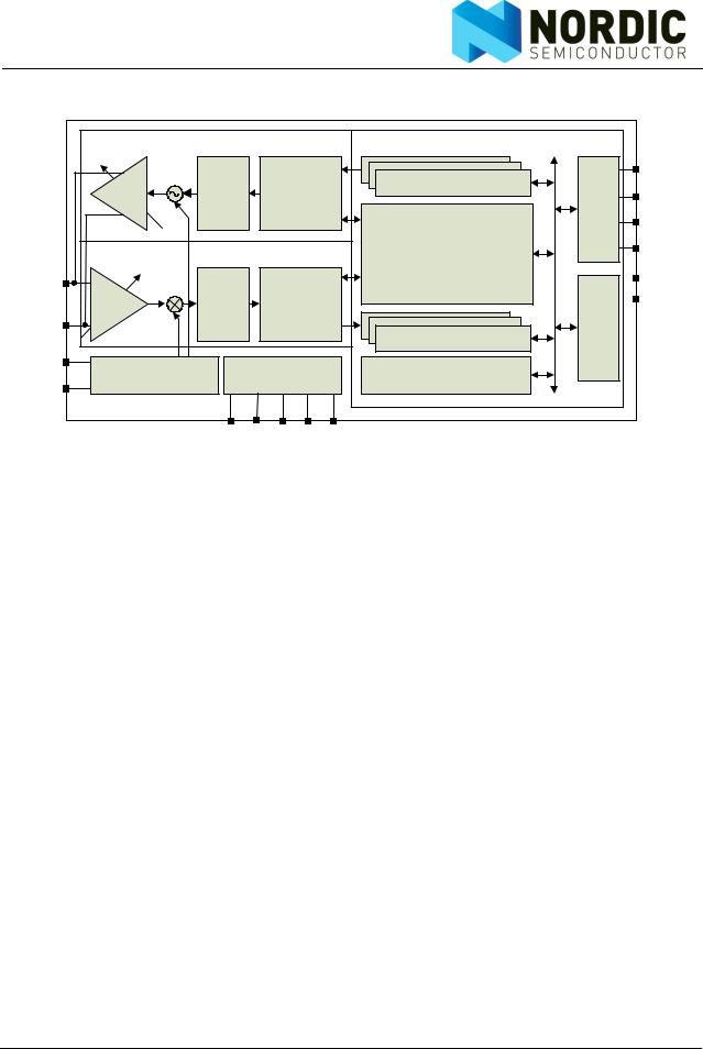
1.2Block diagram
RF Transmitter |
|
|
|
|
Baseband |
|
|
|
|
|
|
|
TX FIFOs |
|
CSN |
PA |
TX |
|
GFSK |
|
|
SCK |
|
|
|
|
|
||||
Filter |
|
Modulator |
|
|
SPI |
||
|
|
|
|
|
|
MISO |
|
|
|
|
|
|
|
|
|
RF Receiver |
|
|
|
|
Enhanced ShockBurst |
|
MOSI |
|
|
|
|
Baseband Engine |
|
|
|
|
|
|
|
|
|
IRQ |
|
ANT1 |
|
|
|
|
|
|
|
RX |
|
GFSK |
|
|
map |
CE |
|
LNA |
|
|
|
||||
Filter |
|
Demodulator |
|
|
|||
ANT2 |
|
|
|
|
RX FIFOs |
Register |
|
|
|
|
|
|
|
||
XC1 |
|
|
|
|
|
|
|
|
|
|
|
|
|
|
|
RF Synthesiser |
Power Management |
Radio Control |
|
|
|||
XC2 |
|
|
|
|
|
|
|
|
VSS |
VDD |
IREF DVDD |
VDD PA |
|
|
|
Figure 1. nRF24L01+ block diagram
Revision 1.0 |
Page 9 of 78 |