


nRF24L01+ Product Specification
8 Data and Control Interface
The data and control interface gives you access to all the features in the nRF24L01+. The data and control interface consists of the following six 5Volt tolerant digital signals:
•IRQ (this signal is active low and controlled by three maskable interrupt sources)
•CE (this signal is active high and used to activate the chip in RX or TX mode)
•CSN (SPI signal)
•SCK (SPI signal)
•MOSI (SPI signal)
•MISO (SPI signal)
Using 1 byte SPI commands, you can activate the nRF24L01+ data FIFOs or the register map during all modes of operation.
8.1 Features
• Special SPI commands for quick access to the most frequently used features
• 0-10Mbps 4-wire SPI
• 8 bit command set
• Easily configurable register map
• Full three level FIFO for both TX and RX direction
8.2 Functional description
The SPI is a standard SPI with a maximum data rate of 10Mbps.
8.3SPI operation
This section describes the SPI commands and timing.
8.3.1SPI commands
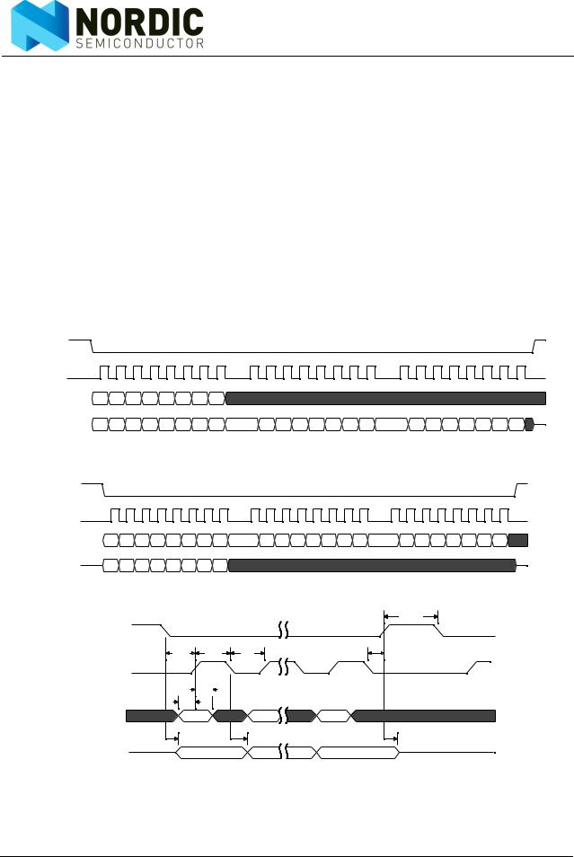
The SPI commands are shown in Table 20. Every new command must be started by a high to low transition on CSN.
The STATUS register is serially shifted out on the MISO pin simultaneously to the SPI command word shifting to the MOSI pin.
The serial shifting SPI commands is in the following format:
<Command word: MSBit to LSBit (one byte)>
<Data bytes: LSByte to MSByte, MSBit in each byte first>
See Figure 26. on page 52 and Figure 27. on page 52 for timing information.
Revision 1.0 |
Page 50 of 78 |
nRF24L01+ Product Specification
Command name |
Command |
# Data bytes |
Operation |
word (binary) |
|||
R_REGISTER |
000A AAAA |
1 to 5 |
Read command and status registers. AAAAA = |
|
|
LSByte first |
5 bit Register Map Address |
W_REGISTER |
001A AAAA |
1 to 5 |
Write command and status registers. AAAAA = 5 |
|
|
LSByte first |
bit Register Map Address |
|
|
|
Executable in power down or standby modes |
|
|
|
only. |
R_RX_PAYLOAD |
0110 0001 |
1 to 32 |
Read RX-payload: 1 – 32 bytes. A read operation |
|
|
LSByte first |
always starts at byte 0. Payload is deleted from |
|
|
|
FIFO after it is read. Used in RX mode. |
W_TX_PAYLOAD |
1010 0000 |
1 to 32 |
Write TX-payload: 1 – 32 bytes. A write operation |
|
|
LSByte first |
always starts at byte 0 used in TX payload. |
FLUSH_TX |
1110 0001 |
0 |
Flush TX FIFO, used in TX mode |
FLUSH_RX |
1110 0010 |
0 |
Flush RX FIFO, used in RX mode |
|
|
|
Should not be executed during transmission of |
|
|
|
acknowledge, that is, acknowledge package will |
|
|
|
not be completed. |
REUSE_TX_PL |
1110 0011 |
0 |
Used for a PTX device |
|
|
|
Reuse last transmitted payload. |
|
|
|
TX payload reuse is active until |
|
|
|
W_TX_PAYLOAD or FLUSH TX is executed. TX |
|
|
|
payload reuse must not be activated or deacti- |
|
|
|
vated during package transmission. |
R_RX_PL_WIDa |
0110 0000 |
1 |
Read RX payload width for the top |
|
|
|
R_RX_PAYLOAD in the RX FIFO. |
|
|
|
Note: Flush RX FIFO if the read value is larger |
|
|
|
than 32 bytes. |
W_ACK_PAYLOADa |
1010 1PPP |
1 to 32 |
Used in RX mode. |
|
|
LSByte first |
Write Payload to be transmitted together with |
|
|
|
ACK packet on PIPE PPP. (PPP valid in the |
|
|
|
range from 000 to 101). Maximum three ACK |
|
|
|
packet payloads can be pending. Payloads with |
|
|
|
same PPP are handled using first in - first out |
|
|
|
principle. Write payload: 1– 32 bytes. A write |
|
|
|
operation always starts at byte 0. |
W_TX_PAYLOAD_NO |
1011 0000 |
1 to 32 |
Used in TX mode. Disables AUTOACK on this |
ACKa |
|
LSByte first |
specific packet. |
NOP |
1111 1111 |
0 |
No Operation. Might be used to read the STATUS |
|
|
|
register |
a. The bits in the FEATURE register shown in Table 28. on page 63 have to be set.
Table 20. Command set for the nRF24L01+ SPI
The W_REGISTER and R_REGISTER commands operate on single or multi-byte registers. When accessing multi-byte registers read or write to the MSBit of LSByte first. You can terminate the writing before all bytes in a multi-byte register are written, leaving the unwritten MSByte(s) unchanged. For example, the LSByte of RX_ADDR_P0 can be modified by writing only one byte to the RX_ADDR_P0 register. The content of the status register is always read to MISO after a high to low transition on CSN.
Revision 1.0 |
Page 51 of 78 |
nRF24L01+ Product Specification
Note: The 3 bit pipe information in the STATUS register is updated during the IRQ pin high to low transition. The pipe information is unreliable if the STATUS register is read during an IRQ pin high to low transition.
8.3.2SPI timing
SPI operation and timing is shown in Figure 26. to Figure 28. and in Table 22. to Table 27.. nRF24L01+ must be in a standby or power down mode before writing to the configuration registers.
In Figure 26. to Figure 28. the following abbreviations are used:
Abbreviation |
Description |
Cn |
SPI command bit |
Sn |
STATUS register bit |
Dn |
Data Bit (Note: LSByte to MSByte, MSBit in each byte first) |
Table 21. Abbreviations used in Figure 26. to Figure 28.
CSN
SCK
MOSI 
MISO 
C7 |
C6 |
C5 |
C4 |
C3 |
C2 |
C1 |
C0 |
|
|
|
|
|
|
|
|
|
|
|
|
|
|
|
|
S7 |
S6 |
S5 |
S4 |
S3 |
S2 |
S1 |
S0 |
D7 |
D6 |
D5 |
D4 |
D3 |
D2 |
D1 |
D0 |
D1 5 |
D1 4 |
D1 3 |
D1 2 |
D1 1 |
D1 0 |
D9 |
D8 |
Figure 26. SPI read operation
CSN
SCK
MOSI 
MISO
C7 |
C6 |
C5 |
C4 |
C3 |
C2 |
C1 |
C0 |
D7 |
D6 |
D5 |
D4 |
D3 |
D2 |
D1 |
D0 |
D1 5 |
D1 4 |
D1 3 |
D1 2 |
D1 1 |
D1 0 |
D9 |
D8 |
S7 |
S6 |
S5 |
S4 |
S3 |
S2 |
S1 |
S0 |
|
|
|
|
|
|
|
|
|
|
|
|
|
|
|
|
Figure 27. SPI write operation
|
|
|
Tcwh |
CSN |
|
|
|
|
Tcc Tch |
Tcl |
Tcch |
SCK |
|
|
|
|
Tdh |
|
|
MOSI |
Tdc |
|
|
C7 |
C6 |
C0 |
Tcsd |
Tcd |
Tcdz |
MISO |
S7 |
S0 |
Figure 28. SPI NOP timing diagram
Revision 1.0 |
Page 52 of 78 |
nRF24L01+ Product Specification
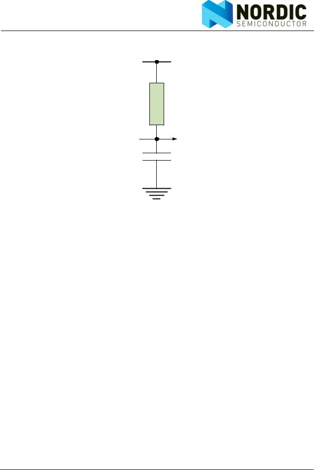
Figure 29. shows the Rpull and Cload that are referenced in Table 22. to Table 27.
Vdd
|
Rpull |
nRF24L01+ pin |
External |
|
Cload |
|
Figure 29. Rpull and Cload |
|
|
||
|
|
|
|
|
|
Symbol |
Parameters |
Min. |
|
Max |
Units |
Tdc |
Data to SCK Setup |
2 |
|
|
ns |
Tdh |
SCK to Data Hold |
2 |
|
|
ns |
Tcsd |
CSN to Data Valid |
|
|
38 |
ns |
Tcd |
SCK to Data Valid |
|
|
55 |
ns |
Tcl |
SCK Low Time |
40 |
|
|
ns |
Tch |
SCK High Time |
40 |
|
|
ns |
Fsck |
SCK Frequency |
0 |
|
10 |
MHz |
Tr,Tf |
SCK Rise and Fall |
|
|
100 |
ns |
Tcc |
CSN to SCK Setup |
2 |
|
|
ns |
Tcch |
SCK to CSN Hold |
2 |
|
|
ns |
Tcwh |
CSN Inactive time |
50 |
|
|
ns |
Tcdz |
CSN to Output High Z |
|
|
38 |
ns |
Table 22. SPI timing parameters (Cload = 5pF)
Symbol |
Parameters |
Min. |
Max |
Units |
Tdc |
Data to SCK Setup |
2 |
|
ns |
Tdh |
SCK to Data Hold |
2 |
|
ns |
Tcsd |
CSN to Data Valid |
|
42 |
ns |
Tcd |
SCK to Data Valid |
|
58 |
ns |
Tcl |
SCK Low Time |
40 |
|
ns |
Tch |
SCK High Time |
40 |
|
ns |
Fsck |
SCK Frequency |
0 |
8 |
MHz |
Tr,Tf |
SCK Rise and Fall |
|
100 |
ns |
Tcc |
CSN to SCK Setup |
2 |
|
ns |
Revision 1.0 |
Page 53 of 78 |

nRF24L01+ Product Specification
Symbol |
Parameters |
Min. |
Max |
Units |
Tcch |
SCK to CSN Hold |
2 |
|
ns |
Tcwh |
CSN Inactive time |
50 |
|
ns |
Tcdz |
CSN to Output High Z |
|
42 |
ns |
Table 23. SPI timing parameters (Cload = 10pF)
Symbol |
Parameters |
Min. |
Max |
|
Units |
Tdc |
Data to SCK Setup |
2 |
|
|
ns |
Tdh |
SCK to Data Hold |
2 |
|
|
ns |
Tcsd |
CSN to Data Valid |
|
75 |
|
ns |
Tcd |
SCK to Data Valid |
|
86 |
|
ns |
Tcl |
SCK Low Time |
40 |
|
|
ns |
Tch |
SCK High Time |
40 |
|
|
ns |
Fsck |
SCK Frequency |
0 |
5 |
|
MHz |
Tr,Tf |
SCK Rise and Fall |
|
100 |
|
ns |
Tcc |
CSN to SCK Setup |
2 |
|
|
ns |
Tcch |
SCK to CSN Hold |
2 |
|
|
ns |
Tcwh |
CSN Inactive time |
50 |
|
|
ns |
Tcdz |
CSN to Output High Z |
|
75 |
|
ns |
|
Table 24. SPI timing parameters (Rpull = 10kΩ, Cload = 50pF) |
|
|||
|
|
|
|
|
|
Symbol |
Parameters |
Min. |
Max |
|
Units |
Tdc |
Data to SCK Setup |
2 |
|
|
ns |
Tdh |
SCK to Data Hold |
2 |
|
|
ns |
Tcsd |
CSN to Data Valid |
|
116 |
|
ns |
Tcd |
SCK to Data Valid |
|
123 |
|
ns |
Tcl |
SCK Low Time |
40 |
|
|
ns |
Tch |
SCK High Time |
40 |
|
|
ns |
Fsck |
SCK Frequency |
0 |
4 |
|
MHz |
Tr,Tf |
SCK Rise and Fall |
|
100 |
|
ns |
Tcc |
CSN to SCK Setup |
2 |
|
|
ns |
Tcch |
SCK to CSN Hold |
2 |
|
|
ns |
Tcwh |
CSN Inactive time |
50 |
|
|
ns |
Tcdz |
CSN to Output High Z |
|
116 |
|
ns |
Table 25. SPI timing parameters (Rpull = 10kΩ, Cload = 100pF)
Revision 1.0 |
Page 54 of 78 |