

- •8-Pin Flash-Based, 8-Bit CMOS Microcontrollers with nanoWatt Technology
- •1.0 Device Overview
- •2.0 Memory Organization
- •2.1 Program Memory Organization
- •FIGURE 2-1: Program Memory Map and Stack for the PIC12F683
- •2.2 Data Memory Organization
- •2.2.1 General Purpose Register File
- •2.2.2 Special Function Registers
- •FIGURE 2-2: Data Memory Map of the PIC12F683
- •2.3 PCL and PCLATH
- •FIGURE 2-3: Loading of PC in Different Situations
- •2.3.2 Stack
- •2.4 Indirect Addressing, INDF and FSR Registers
- •EXAMPLE 2-1: Indirect Addressing
- •3.1 Overview
- •FIGURE 3-1: PIC® MCU Clock Source Block Diagram
- •3.2 Oscillator Control
- •3.3 Clock Source Modes
- •3.4 External Clock Modes
- •TABLE 3-1: Oscillator Delay Examples
- •3.4.2 EC Mode
- •FIGURE 3-2: External Clock (EC) Mode Operation
- •3.4.3 LP, XT, HS Modes
- •FIGURE 3-3: Quartz Crystal Operation (LP, XT or HS Mode)
- •3.4.4 External RC Modes
- •FIGURE 3-5: External RC Modes
- •3.5 Internal Clock Modes
- •3.5.1 INTOSC and INTOSCIO Modes
- •3.5.2 HFINTOSC
- •3.5.3 LFINTOSC
- •3.5.4 Frequency Select Bits (IRCF)
- •3.5.5 HF and LF INTOSC Clock Switch Timing
- •FIGURE 3-6: Internal Oscillator Switch Timing
- •3.6 Clock Switching
- •3.6.1 System Clock Select (SCS) Bit
- •FIGURE 3-7: Two-Speed Start-up
- •FIGURE 3-8: FSCM Block Diagram
- •4.0 GPIO Port
- •4.1 GPIO and the TRISIO Registers
- •4.2 Additional Pin Functions
- •4.2.1 ANSEL Register
- •4.2.3 Interrupt-on-Change
- •Register 4-3: ANSEL: Analog Select Register
- •4.2.5 Pin Descriptions and Diagrams
- •FIGURE 4-1: Block Diagram of GP0
- •FIGURE 4-2: Block Diagram of GP1
- •FIGURE 4-4: Block Diagram of GP3
- •FIGURE 4-5: Block Diagram of GP4
- •FIGURE 4-6: Block Diagram of GP5
- •5.0 Timer0 Module
- •5.1 Timer0 Operation
- •FIGURE 5-1: Block Diagram of the Timer0/WDT Prescaler
- •5.1.3 Software Programmable Prescaler
- •5.1.4 Timer0 Interrupt
- •5.1.5 Using Timer0 with an External Clock
- •6.0 Timer1 Module with Gate Control
- •6.1 Timer1 Operation
- •6.2 Clock Source Selection
- •FIGURE 6-1: Timer1 Block Diagram
- •6.2.1 iNternal Clock Source
- •6.2.2 External Clock Source
- •6.3 Timer1 Prescaler
- •6.4 Timer1 Oscillator
- •6.5 Timer1 Operation in Asynchronous Counter Mode
- •6.5.1 Reading and Writing Timer1 in Asynchronous Counter Mode
- •6.6 Timer1 Gate
- •6.7 Timer1 Interrupt
- •6.8 Timer1 Operation During Sleep
- •6.9 CCP Special Event Trigger
- •6.10 Comparator Synchronization
- •FIGURE 6-2: Timer1 Incrementing Edge
- •6.11 Timer1 Control Register
- •7.0 Timer2 Module
- •7.1 Timer2 Operation
- •FIGURE 7-1: Timer2 Block Diagram
- •8.0 Comparator Module
- •8.1 Comparator Overview
- •FIGURE 8-1: Single Comparator
- •FIGURE 8-2: Comparator Output Block Diagram
- •8.2 Analog Input Connection Considerations
- •8.3 Comparator Configuration
- •8.4 Comparator Control
- •8.4.1 Comparator Output State
- •8.4.2 Comparator Output Polarity
- •8.4.3 Comparator Input Switch
- •8.5 Comparator Response Time
- •8.6 Comparator Interrupt Operation
- •8.7 Operation During Sleep
- •8.8 Effects of a Reset
- •8.9 Comparator Gating Timer1
- •8.10 Synchronizing Comparator Output to Timer1
- •8.11 Comparator Voltage Reference
- •8.11.1 Independent Operation
- •8.11.2 Output Voltage Selection
- •EQUATION 8-1: CVref Output Voltage
- •8.11.4 Output Ratiometric to Vdd
- •FIGURE 8-7: Comparator Voltage Reference Block Diagram
- •TABLE 8-2: Summary of Registers Associated with the Comparator and Voltage Reference Modules
- •FIGURE 9-1: ADC Block Diagram
- •9.1 ADC Configuration
- •9.1.1 GPIO Configuration
- •9.1.2 Channel Selection
- •9.1.4 Conversion Clock
- •FIGURE 9-2: Analog-to-Digital Conversion Tad Cycles
- •9.1.5 Interrupts
- •9.1.6 Result Formatting
- •9.2 ADC Operation
- •9.2.1 Starting a Conversion
- •9.2.2 Completion of a Conversion
- •9.2.3 Terminating a conversion
- •9.2.4 ADC Operation During Sleep
- •9.2.5 Special Event Trigger
- •9.2.6 A/D Conversion Procedure
- •EXAMPLE 9-1: A/D Conversion
- •9.2.7 ADC Register Definitions
- •9.3 A/D Acquisition Requirements
- •EQUATION 9-1: Acquisition Time Example
- •FIGURE 9-5: ADC Transfer Function
- •10.0 Data EEPROM Memory
- •10.1 EECON1 and EECON2 Registers
- •EXAMPLE 10-1: DATA EEPROM READ
- •EXAMPLE 10-2: DATA EEPROM WRITE
- •10.4 Write Verify
- •EXAMPLE 10-3: WRITE VERIFY
- •10.4.1 Using the Data EEPROM
- •10.5 Protection Against Spurious Write
- •TABLE 10-1: Summary of Associated Data EEPROM Registers
- •11.0 Capture/Compare/PWM (CCP) Module
- •TABLE 11-1: CCP Mode – Timer Resources Required
- •11.1 Capture Mode
- •11.1.1 CCP1 pin Configuration
- •11.1.2 Timer1 Mode Selection
- •11.1.3 Software Interrupt
- •11.1.4 CCP Prescaler
- •11.2 Compare Mode
- •11.2.1 CCP1 Pin Configuration
- •11.2.2 timer1 Mode Selection
- •11.2.3 Software Interrupt Mode
- •11.2.4 Special Event Trigger
- •11.3 PWM Mode
- •FIGURE 11-3: Simplified PWM Block Diagram
- •FIGURE 11-4: CCP PWM Output
- •11.3.1 PWM period
- •EQUATION 11-1: PWM Period
- •11.3.2 PWM Duty Cycle
- •EQUATION 11-2: Pulse Width
- •EQUATION 11-3: Duty Cycle Ratio
- •11.3.3 PWM Resolution
- •EQUATION 11-4: PWM Resolution
- •11.3.4 Operation in Sleep Mode
- •11.3.5 Changes in System Clock Frequency
- •11.3.6 Effects of Reset
- •11.3.7 Setup for PWM Operation
- •TABLE 11-4: Registers Associated with Capture, cOMPARE and Timer1
- •12.0 Special Features of the CPU
- •12.1 Configuration Bits
- •12.2 Calibration Bits
- •12.3 Reset
- •FIGURE 12-1: Simplified Block Diagram of On-Chip Reset Circuit
- •12.3.2 MCLR
- •FIGURE 12-2: Recommended MCLR Circuit
- •12.3.5 BOR Calibration
- •12.3.7 Power Control (PCON) Register
- •TABLE 12-1: Time-out in Various Situations
- •TABLE 12-2: Status/PCON Bits and Their Significance
- •TABLE 12-3: Summary of Registers Associated with Brown-out Reset
- •FIGURE 12-4: Time-out Sequence on Power-up (Delayed MCLR)
- •FIGURE 12-5: Time-out Sequence on Power-up (Delayed MCLR)
- •FIGURE 12-6: Time-out Sequence on Power-up (MCLR with Vdd)
- •TABLE 12-5: Initialization Condition for Special Registers
- •12.4 Interrupts
- •12.4.1 GP2/INT Interrupt
- •12.4.2 Timer0 Interrupt
- •12.4.3 GPIO Interrupt
- •FIGURE 12-7: Interrupt Logic
- •TABLE 12-6: Summary of Registers Associated with Interrupts
- •12.5 Context Saving During Interrupts
- •12.6 Watchdog Timer (WDT)
- •12.6.1 WDT Oscillator
- •12.6.2 WDT Control
- •TABLE 12-7: WDT Status
- •TABLE 12-8: Summary of Registers Associated with Watchdog Timer
- •12.8 Code Protection
- •12.9 ID Locations
- •12.10 In-Circuit Serial Programming™
- •FIGURE 12-11: Typical In-Circuit Serial Programming Connection
- •12.11 In-Circuit Debugger
- •TABLE 12-9: Debugger Resources
- •FIGURE 12-12: 14-Pin ICD Pinout
- •13.0 Instruction Set Summary
- •13.2 Instruction Descriptions
- •14.0 Development Support
- •14.1 MPLAB Integrated Development Environment Software
- •14.2 MPASM Assembler
- •14.3 MPLAB C18 and MPLAB C30 C Compilers
- •14.4 MPLINK Object Linker/ MPLIB Object Librarian
- •14.5 MPLAB ASM30 Assembler, Linker and Librarian
- •14.6 MPLAB SIM Software Simulator
- •14.10 MPLAB PM3 Device Programmer
- •14.11 PICSTART Plus Development Programmer
- •14.12 PICkit 2 Development Programmer
- •14.13 Demonstration, Development and Evaluation Boards
- •15.0 Electrical Specifications
- •FIGURE 15-2: HFINTOSC Frequency Accuracy Over Device Vdd and Temperature
- •15.6 Thermal Considerations
- •15.7 Timing Parameter Symbology
- •FIGURE 15-3: Load Conditions
- •15.8 AC Characteristics: PIC12F683 (Industrial, Extended)
- •TABLE 15-1: Clock Oscillator Timing Requirements
- •TABLE 15-2: Oscillator Parameters
- •FIGURE 15-5: CLKOUT and I/O Timing
- •TABLE 15-3: CLKOUT and I/O Timing Parameters
- •FIGURE 15-6: Reset, Watchdog Timer, Oscillator Start-up Timer and Power-up Timer Timing
- •FIGURE 15-7: Brown-out Reset Timing and Characteristics
- •FIGURE 15-8: Timer0 and Timer1 External Clock Timings
- •TABLE 15-5: Timer0 and Timer1 External Clock Requirements
- •FIGURE 15-9: Capture/Compare/PWM Timings (ECCP)
- •TABLE 15-6: Capture/Compare/PWM Requirements (ECCP)
- •TABLE 15-7: Comparator Specifications
- •TABLE 15-8: Comparator Voltage Reference (CVref) Specifications
- •TABLE 15-9: PIC12F683 A/D Converter (ADC) Characteristics
- •TABLE 15-10: PIC12F683 A/D Conversion Requirements
- •FIGURE 15-10: PIC12F683 A/D Conversion Timing (Normal Mode)
- •FIGURE 15-11: PIC12F683 A/D Conversion Timing (Sleep Mode)
- •16.0 DC and AC Characteristics Graphs and Tables
- •FIGURE 16-1: Typical Idd vs. Fosc Over Vdd (EC Mode)
- •FIGURE 16-2: Maximum Idd vs. Fosc Over Vdd (EC Mode)
- •FIGURE 16-3: Typical Idd vs. Fosc Over Vdd (HS Mode)
- •FIGURE 16-4: Maximum Idd vs. Fosc Over Vdd (HS Mode)
- •FIGURE 16-5: Typical Idd vs. Vdd Over Fosc (XT Mode)
- •FIGURE 16-6: Maximum Idd vs. Vdd Over Fosc (XT Mode)
- •FIGURE 16-7: Typical Idd vs. Vdd Over Fosc (EXTRC Mode)
- •FIGURE 16-8: Maximum Idd vs. Vdd (EXTRC Mode)
- •FIGURE 16-9: Idd vs. Vdd Over Fosc (LFINTOSC Mode, 31 kHz)
- •FIGURE 16-10: Idd vs. Vdd (LP Mode)
- •FIGURE 16-11: Typical Idd vs. Fosc Over Vdd (HFINTOSC Mode)
- •FIGURE 16-12: Maximum Idd vs. Fosc Over Vdd (HFINTOSC Mode)
- •FIGURE 16-13: Typical Ipd vs. Vdd (Sleep Mode, all Peripherals Disabled)
- •FIGURE 16-14: Maximum Ipd vs. Vdd (Sleep Mode, all Peripherals Disabled)
- •FIGURE 16-15: Comparator Ipd vs. Vdd (Both Comparators Enabled)
- •FIGURE 16-16: BOR Ipd VS. Vdd Over Temperature
- •FIGURE 16-17: Typical WDT Ipd VS. Vdd Over Temperature
- •FIGURE 16-18: Maximum WDT Ipd VS. Vdd Over Temperature
- •FIGURE 16-19: WDT Period VS. Vdd Over Temperature
- •FIGURE 16-20: WDT Period VS. Temperature Over Vdd (5.0V)
- •FIGURE 16-21: CVref Ipd VS. Vdd Over Temperature (High Range)
- •FIGURE 16-22: CVref Ipd VS. Vdd Over Temperature (Low Range)
- •FIGURE 16-23: Vol VS. Iol Over Temperature (Vdd = 3.0V)
- •FIGURE 16-24: Vol VS. Iol Over Temperature (Vdd = 5.0V)
- •FIGURE 16-25: Voh VS. Ioh Over Temperature (Vdd = 3.0V)
- •FIGURE 16-26: Voh VS. Ioh Over Temperature (Vdd = 5.0V)
- •FIGURE 16-27: TTL Input Threshold Vin VS. Vdd Over Temperature
- •FIGURE 16-28: Schmitt Trigger Input Threshold Vin VS. Vdd Over Temperature
- •FIGURE 16-29: T1OSC Ipd vs. Vdd Over Temperature (32 kHz)
- •FIGURE 16-30: Comparator Response Time (Rising Edge)
- •FIGURE 16-31: Comparator Response Time (Falling Edge)
- •FIGURE 16-32: LFINTOSC Frequency vs. Vdd Over Temperature (31 kHz)
- •FIGURE 16-33: ADC Clock Period vs. Vdd Over Temperature
- •FIGURE 16-34: Typical HFINTOSC Start-Up Times vs. Vdd Over Temperature
- •FIGURE 16-36: Minimum HFINTOSC Start-Up Times vs. Vdd Over Temperature
- •17.0 Packaging Information
- •17.1 Package Marking Information
- •17.2 Package Details
- •Appendix A: Data Sheet Revision History
- •Appendix B: Migrating From Other PIC® Devices
- •INDEX
- •The Microchip Web Site
- •Customer Change Notification Service
- •Customer Support
- •Reader Response
- •Product Identification System
- •Worldwide Sales and Service
PIC12F683
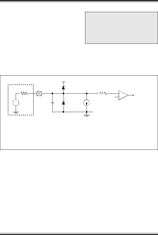
8.2Analog Input Connection Considerations
A simplified circuit for an analog input is shown in Figure 8-3. Since the analog input pins share their connection with a digital input, they have reverse biased ESD protection diodes to VDD and VSS. The analog input, therefore, must be between VSS and VDD. If the input voltage deviates from this range by more than 0.6V in either direction, one of the diodes is forward biased and a latch-up may occur.
A maximum source impedance of 10 kΩ is recommended for the analog sources. Also, any external component connected to an analog input pin, such as a capacitor or a Zener diode, should have very little leakage current to minimize inaccuracies introduced.
Note 1: When reading a PORT register, all pins configured as analog inputs will read as a ‘0’. Pins configured as digital inputs will convert as an analog input, according to the input specification.
2:Analog levels on any pin defined as a digital input, may cause the input buffer to consume more current than is specified.
FIGURE 8-3: |
ANALOG INPUT MODEL |
|
||
|
|
VDD |
|
|
Rs < 10K |
|
VT ≈ 0.6V |
RIC |
|
|
|
|||
|
AIN |
|
To ADC Input |
|
|
|
ILEAKAGE |
||
VA |
CPIN |
VT ≈ 0.6V |
||
5 pF |
±500 nA |
|||
|
||||
|
|
|
Vss |
|
Legend: CPIN |
= Input Capacitance |
ILEAKAGE = Leakage Current at the pin due to various junctions |
|
RIC |
= Interconnect Resistance |
RS |
= Source Impedance |
= Analog Voltage
= Threshold Voltage
DS41211D-page 52 |
♥ 2007 Microchip Technology Inc. |