


Chin. Phys. B Vol. 22, No. 5 (2013) 057701
as shown in Fig. 9(a). In the experiment, a spray-deposited graphene was used to prepare the gauge sensor. They calculated the resistance of the whole flake network by using the Kirchhoff equations. The effect of strain was implemented by displacing the flakes according to the elongation of the whole device and recalculating the network resistance. When the strain was applied, the connected joints among graphene sheets decreased, so the conductive paths reduced. Figure 9(b) demonstrates how the sensitivity of graphene was affected by the morphology of the graphene film. The device with a lower flake number density n exhibited a larger slope in the resistance–strain relationship. The gauge factors were proportional to their original resistances, as shown in the inset of Fig. 9(b). Recently, the graphene woven fabrics (GWFs) was reported for strain sense application,[51] in which the polycrystalline structures changed along with high-density crack formation and propagation when a strain was applied, which is different from pure graphene films. They found that the overlapped area between two graphene sheets changed in width size when the substrate was stretched (Fig. 10(a)). The change of the electrical network of GWF, rather than the deformation of each graphene sheet, was the main reason causing the resistance increase, as shown in Fig. 10(b). When the stress was applied on the device, there were many cracks in the network, which led to the current pathways decrease and the resistance increase, as shown in Fig. 10(c). The resistance change versus the applied strain of different configurations is shown in Fig. 10(d). It is found that a large strain can be easily sustained for graphene microribbons (GMRs) with increased resistors in which there are more conductive pathways.
3.3.Graphene strain sensors based on tunneling effect between neighboring graphene sheets
Even though the gauge factor of the strain sensor based on the over connected graphene is increased to some extent, however, the linear relationship between resistance change and strain limits the gauge factor to be less than 200. As we all know, the distance between two graphene sheets determines the current conduction mode. According to the model shown in Fig. 11, a current can flow between electrodes due to the tunneling effect from one isolated graphene sheet to another, and it is predicted that the resistance changes exponentially with the distance.[52] So the tunneling effect between neighboring graphene sheets can be used for higher GF strain sensors. Our group utilized a homemade PECVD to grow graphene films which consisted of packed graphene nano islands.[53] Through controlling the growing condition, a passel of graphene films could be obtained with different sheet resistances, in which the distance between neighboring
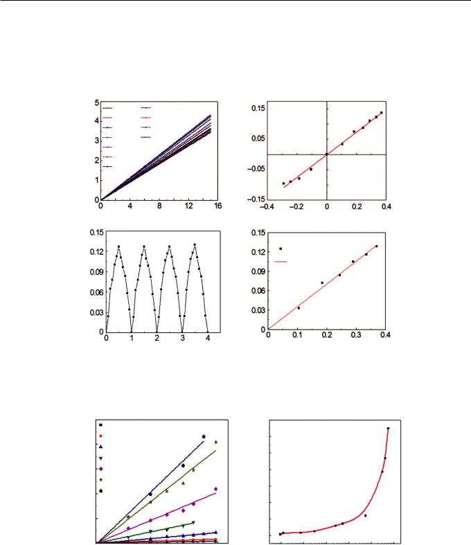
graphene nano islands was variable as shown by the varied sheet resistance. The piezoresistive sensitivity of a graphene device obtained after a series of micro-fabrication processes is shown in Fig. 12(a), in which the current increases obviously as the strain changes from 0.29% to 0.37%. This is mainly caused by the increased tunneling distance among different nanographene islands with the strain applied. From the resistance plot in Fig. 12(b), it is found that the gauge factor is about 37. This nanographene based strain sensor presented a good reliability in several tests, as shown in Fig. 12(c). According to the tunneling model, the relation between resistance RI and tunneling distance d can be writ-
|
RI = ( |
8phL |
Xd |
, where X = 4p(2mf) |
1/2 |
/h, and |
|
ten as |
|
) e |
|
|
|||
3A2XdN |
|
|
|||||
h, L, N, A2, and f are the Plank’s constant, the number of particles forming a single conducting path, the number of conducting paths, the effective cross-section, and the height of potential barrier between adjacent particles, respectively. Through calculation we find ln(R/R0) = ln(1 + e) + Xd0e. In Fig. 12(d), when deformation e < 0.4% with R0 = 1.9 MW, the distance between two nanographene islands is estimated to be 3.4 nm. The nanographene with different thickness and conductivity was studied systematically, and a nearly inversely proportional correlation was found and is shown in Fig. 13(b). The resistance increased obviously when the strain was added from 0 to 0.3% as shown in Fig. 13(a), and a gauge factor over 300, the highest so far for graphenebased strain sensors, was obtained. This tunneling based strain sensor gives us a new way to explore more sensitive and commercial products. Besides, the graphene embedded polymer composition system is also used for the strain sensor, in which the tunneling mechanism and certain effect of the overlapping change coexist. An Indian group used the reduced graphite oxide embedded in a polymer to synthesize conductive graphene-polymer composites.[54] In Fig. 14(a), we can see that the 2.2 wt.% reduced graphite oxide– polyvinylidenefluoride (PVDF) film responds to the strain and its gauge factor is 12.1. The fatigue and repeatability test results are shown in Figs. 14(c)–14(e), which demonstrate the
|
stress |
|
electrode |
|
conducting filler |
current |
|
flow |
conducting path |
|
polymer matrix |
Fig. 11. Schematic illustration of the tunneling model.[52]
057701-6
Chin. Phys. B Vol. 22, No. 5 (2013) 057701
flexibility of the graphene–polymer composite. In that case, both the tunneling effect and the loss of conductive interconnections between neighboring fillers play more important roles compared with the resistance change caused by the graphene deformation. According to the scale of gauge factor, we can
imagine that the change of overlapping between neighboring sheets rather than the tunneling effect dominates. Besides, the sensitivity of the strain sensor based on a graphene composite reflects not only the properties of the graphene but also the whole system features such as the graphene proportion.
Current/nA
DR/R0
-0.29% |
0.245% |
(a) |
-0.245% |
0.29% |
|
-0.185% |
0.335% |
|
-0.105% |
0.37% |
|
0% |
0 |
|
DR/R |
||
0.185% |
||
0.105% |
|
Voltage/V
(c)
ln(R/R0)
Cycle
(b)GF=37
Strain/%
(d)
data points linear fit
Strain/%
Fig. 12. (color online) Piezoelectricity of the nanographene-based strain sensors. (a) The I–V curve of a device with original sheet resistance of 5.5 MW under different strains. (b) Resistance modulation of the device showing a GF 37. Both experimental data and line fit are shown. (c) Multi-cycle operation of the device. (d) The relation between resistance changes and applied strains. The points and line show the experimental data and fitting, respectively.[53]
DR/R0
1.0
R0=9.3 kW (a) R0=74 kW
0.8R0=2.7 kW
R0=37.5 kW
0.6R0=322 kW R0=423 kW
0.4R0=575 kW
0.2
0
0 |
0.1 |
0.2 |
0.3 |
Strain/%
Gauge factor
(b)
300
200
100
0
104 |
106 |
108 |
|
R0 |
|
Fig. 13. (color online) Tunable gauge factors for graphene-based strain sensors. (a) Strain induced resistance changes for devices with different sheet resistances, where the points and lines show the experimental and linear fit data, respectively. (b) Gauge factor versus sheet resistance.[53]
057701-7