

Chin. Phys. B Vol. 22, No. 5 (2013) 057701
REVIEW
Review of graphene-based strain sensors
Zhao Jing( )a)b), Zhang Guang-Yu( )b), and Shi Dong-Xia( )b)†
a)Renmin University of China, Department of Physics, Beijing 100872, China
b)Nanoscale Physics and Device Laboratory, Beijing National Laboratory for Condensed Matter Physics and Institute of Physics,
Chinese Academy of Sciences, Beijing 100190, China
(Received 4 February 2013; revised manuscript received 13 March 2013)
In this paper, we review various types of graphene-based strain sensors. Graphene is a monolayer of carbon atoms, which exhibits prominent electrical and mechanical properties and can be a good candidate in compact strain sensor applications. However, a perfect graphene is robust and has a low piezoresistive sensitivity. So scientists have been driven to increase the sensitivity using different kinds of methods since the first graphene-based strain sensor was reported. We give a comprehensive review of graphene-based strain sensors with different structures and mechanisms. It is obvious that graphene offers some advantages and has potential for the strain sensor application in the near future.
Keywords: graphene, strain sensor, gauge factor
PACS: 77.65.Ly, 81.15.Gh, 81.40.Lm, 73.61.Wp
1. Introduction
Since Thomson first reported on the change in resistance with elongation in iron and copper in 1856, strain sensors have been widely fabricated by employing various metals and semiconductors.[1–6] The resistance R, a characteristic of a conductor, can be written as R = rL/S, where L is the length and S is the average cross-sectional area of the conductor. When a stress is applied to the conductor, its resistance changes. Besides the geometry, the resistivity change also plays an important role in resistance change. The crosssectional area of a bulk material reduces in proportion to the longitudinal strain with Poisson’s ratio n. The Poisson’s ratio ranges from 0.20 to 0.35 for most metals, while it ranges from 0.06 to 0.36 for anisotropic silicon.[7,8] The isotropic lower and upper limits of n are 1.0 and 0.5, respectively. The gauge factor (GF) is a common figure to show the sensitivity of electrical shift to mechanical deformation. The relation between the change in electrical resistance and the applied strain is revealed by GF = (DR/R)/e, where DR/R is the normalized resistance variation, and e is the mechanical strain. The resistance change is dependent on both geometry and resistivity as DR/R = (1 + 2n)e + Dr/r.[9] According to the above function, we can see that the effect of geometric deformation alone provides a GF of approximately 1.4 to 2.0. However, for a metal, the resistivity change Dr/r (of the order of 0.3) is smaller compared with that of semiconductors, as in silicon and germanium, Dr/r is 50–100 times larger than the geometric term.
The strain sensor market is expected to exceed 4.5 billion US dollars in 2013. Along with the relentless pursuit of low-cost and miniaturized devices, the traditional silicon
DOI: 10.1088/1674-1056/22/5/057701
semiconductor faces challenges, recent research of strain sensors is focused on nanoscale materials. One of the most compelling materials is the low-dimensional carbon.[10–14] Carbon nanotubes (CNTs) and graphene are two examples in the carbon family which have attracted enormous attention in recent years due to their wonderful mechanical and electrical properties for piezoresistive strain sensors. Compared to CNTs with the quasi one-dimensional (1D) structure, graphene has an ideal two-dimensional (2D) structure, thus has advantages in scalable device fabrication via top-down approaches, which is compatible with the existing semiconductor fabrication technology. Compared with other material based strain sensors, this ultra-thin transparent graphene device is more commercial and easily obtained. The schematic structure of a graphene strain sensor is shown in Fig. 1, and it includes two electrodes in each side of the graphene.[15] When a stress is applied on it, a resistance change can be observed. In this paper, we mainly discuss the graphene-based strain gauge with different mechanisms of piezoelectricity.
A
εyy |
ε |
|
xx |
L
Fig. 1. (color online) Schematic diagram of a strain sensor based on graphene.[15]
Project supported by the National Basic Research Program of China (Grant No. 2013CB934500) and the National Natural Science Foundation of China (Grant No. 91223204).
†Corresponding author. E-mail: dxshi@aphy.iphy.ac.cn
© 2013 Chinese Physical Society and IOP Publishing Ltd |
http://iopscience.iop.org/cpb http://cpb.iphy.ac.cn |
057701-1

Chin. Phys. B Vol. 22, No. 5 (2013) 057701
2.Electronic and mechanical properties of graphene
Graphene has attracted tremendous attention since its first isolation by Geim and Novoselov in 2004.[16–19] It is densely packed by sp2 carbon atoms and can be rolled up to form zerodimensional fullerene and 1D carbon nanotube. Because of the structure, the carrier dynamics is strictly confined in a 2D layer. The honeycomb lattice has two equivalent lattice sites
A and B, as shown in Fig. 2(a), leading to special electron hopping. For the monolayer graphene, the electronic band structure according to the results of the tight-binding model is shown in Fig. 2(b). The valence and conduction bands of graphene are conical valleys that touch at the Dirac points K
and K0 in the Brillouin zone. Near the Dirac point, the carrier has a linear dispersion relation E = hv¯ Fk, so it can be called the massless Dirac fermion. The velocity of electrons in graphene is 106 m/s, about 1/300 of the velocity of light. The bilayer graphene is also a zero band-gap semiconductor, but its electronic dispersion is not linear near the Dirac point. For more than three-layer graphene, the energy band structure becomes more complicated, and the valence and conduction bands begin to overlap. Due to its special electronic band structure, graphene contains rich and novel physical phenomena and properties, such as ultrahigh mobility, ballistic transport, anomalous quantum Hall effect,[20] non-zero minimum quantum conductivity,[21] Anderson weak local change,[22] and Klein tunneling.
(a)
A B
±3 ±2 a1 ±1
a2
(b)
Ek
ky
kx
Fig. 2. (color online) Graphene band structure. (a) Graphene lattice structure. Each original cell contains two symmetrical and inequitable carbon atoms A abd B, and 1 and 2 are the lattice vectors. (b) Graphene electronic band structure obtained in the tight-binding model; the valence and conduction bands connect in the Brillouin area.
The ever-increasing interest in graphene is driven not only by its unusual physical properties but also by its potential for developing sensors of various types. Its mechanical stiffness is 1 TPa, and the intrinsic breaking strength is 130 GPa at 25% strain which is comparable to the remarkable inplane values of graphite and other materials with great mechanical strengths.[23] Today there are many studies focused on the methods to obtain graphene. Micro-mechanically cleaved graphene is widely used for the fundamental research due to its quality, the closest to the nature of graphene. Reducing graphene oxide is an inexpensive and high-efficiency method of graphene synthesis.[24,25] Epitaxial growth on silicon carbide (SiC) can get a wide range of graphene.[26] Chemical vapor deposition (CVD) gives a way on catalytic metal surfaces by surface precipitation or dissociation, allowing the scaledup production of graphene.[27–29] Besides, direct depositing graphene on a substrate without catalytic, such as plasma enhanced chemical vapor deposition (PECVD)[30] and spraydeposited graphene from solution[31], have attracted much attention. Different graphene growth methods have their advantages and disadvantages which satisfy diverse demands. Due to the different growth methods, the graphene quality varies, leading to different mechanisms of strain sensors.
3.Different types of graphene-based strain sensors
3.1.Graphene strain sensors based on structure deformation
Graphene, a truly two-dimensional gapless semiconductor, known as the strongest material ever measured, can sustain up to 25% in-plane tensile elastic strains. A strain, leading to a significant elongation of the graphene, is likely to shift its electronic band structure and cause attractive changes of the electrical properties, resulting in notable electrical– mechanical coupling. Recently, several theoretical calculations on strained graphene indicated that the Dirac cones are shifted and the Fermi velocity is reduced due to the asymmetrical strain distribution in the graphene, which introduces a pseudo-magnetic field and can be used to engineer the electronic structure, while a symmetrical strain distribution cannot change the graphene properties,[32–38] even though the strain can cause additional scattering and resistance decrease. For a strain parallel to the C–C bonds, with the strain increasing to 12.2%, the band gap continuously increases to its maximum of 0.486 eV. While the band gap only continuously increases to a maximum of 0.170 eV when the strain is perpendicular to the C–C bonds and increases up to 7.3%.[39] Moreover, it
057701-2
Chin. Phys. B Vol. 22, No. 5 (2013) 057701
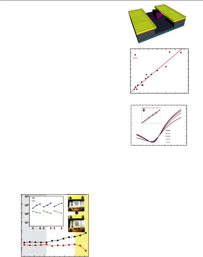
is also suggested in theory that uniaxial strains higher than 23% are needed to open the band gap of graphene. On the experimental side, a CVD grown graphene by one Korea group was transferred onto the flexible substrate polydimethylsiloxane (PDMS), which showed no appreciable resistance change when applying a strain up to 6%, as shown in Fig. 3,[40] which is consistent with the calculation results. To study how the strain works on graphene, Raman spectroscopy is usually used to observe the disruption of graphene symmetry and the band gap opening.[41–43] Scanning tunneling microscopy (STM) studies have also conveyed that a strained graphene with strong gauge fields can cause the pseudo-magnetic quantum Hall effect.[44,45] Direct electrical measurement of suspending strained graphene is needed to eliminate the influences caused by the graphene–substrate interaction and the graphene–dopant coupling. Huang et al. demonstrated that the suspended graphene devices were homogeneous by in situ nanoindentation, while electrical measurements were carried out simultaneously,[46] as shown in Fig. 4(a). They found that even with a larger deformation, the device resistance changed little (Fig. 4(b)) and the gauge factor was 1.9. The electronic transport measurement in Fig. 4(c) indicates that there was no band gap opening when the graphene was under a moderate uniform strain. The resistivity is proportional to the inverse of the square of Fermi velocity vF. So the relationship between resistance and resistivity variation can be written as DR/R = (1 + 2v)e + Dr/r = (1 + 2v)e 2DvF/vF. According to this formula, the calculated gauge factor is 2.4, which is consistent with the experimental result 1.9. However, in order to know whether the structure deformation of graphene can affect the band gap or not, a direct way to demonstrate the band gap opening in a strained graphene with a much larger stress is needed.
|
|
|
Ry |
|
|
|
|
107 |
Resistance/W |
Rx |
|
|
y |
Resistance/W |
|
|
|
|||
|
|
|
|
Ry |
||
|
|
|
|
|
|
x |
|
|
|
1st |
2nd |
3rd |
|
|
105 |
|
stretching cycles |
y |
||
|
|
|
|
|
|
|
|
|
|
Stretching/% |
|
x |
|
|
|
|
|
|
||
|
103 |
|
|
|
|
|
|
|
|
|
|
|
Rx |
|
|
|
stable |
|
|
|
|
101 |
0 |
|
10 |
20 |
30 |
|
|
|
||||
Stretching/%
Fig. 3. (color online) Resistance of a graphene film transferred to a PDMS substrate isotropically stretched by 12%. The left inset shows the case in which the graphene film is transferred to an unstretched PDMS substrate. The right inset shows the movement of holding stages and the consequent change in the shape of the graphene film.[40]
(a)
5experiment data
linear fit |
(b) |
4
)/% 3
R/R 2 (D
1gauge factor b1.9
|
0 |
|
|
|
|
|
|
0 |
|
1.0 |
2.0 |
|
3.0 |
|
|
|
Strain ε/% |
|
|
|
|
0.40 |
0.6 |
experament data |
(c) |
|
|
|
|
|
||||
|
|
calculated data |
|
|
||
|
0 |
|
|
|
|
|
Conductance/mS |
C/CD |
0.4 |
|
|
|
|
|
|
|
|
|
||
|
0.35 |
0.2 |
|
|
|
|
|
|
|
|
|
|
|
|
0.30 |
00 |
0.4 |
0.8 |
|
|
|
0.25 |
|
Strain ε/% |
|
|
|
|
|
|
|
ε=0% |
|
|
|
Vbias=10 mV |
ε=0.36% |
||||
|
0.20 |
|
|
|
ε=0.57% |
|
|
|
|
|
|
ε=0.75% |
|
|
0.15 |
|
|
|
ε=0.93% |
|
|
|
|
|
|
|
|
|
-20 |
|
-10 |
0 |
10 |
20 |
|
|
|
Gate voltage/V |
|
||
Fig. 4. (color online) (a) Schematic diagram of a suspended graphene device with a wedge tip indenting the graphene ribbon. (b) Relative change of resistance as a function of strain. (c) Electrical transport measurement of strained graphene. The inset shows the relative changes of the gate capacitance as a function of strain from the experiment data (red) and a calculation (blue).[46]
There are many other experimental groups that have obtained graphene strain sensors with a high gauge factor, which seems to disaccord with the theoretical calculation showing that perfect graphene has little resistance change under strain. The first group used a wafer-size graphene prepared by CVD growth on Ni and Cu metal films, which was transferred onto arbitrary substrates through instantaneous etching of metal layers to fabricate a strain sensor device, as shown in Fig. 5(a).[47] The piezoelectricity of the device is shown in Fig. 5(b), the resistance changed from 492 kW to 522 kW with applied strain 1%, and the gauge factor was 6.1. The recent research of Yu’s group found that the transferred graphene on PDMS grown by CVD has a higher gauge factor151, as shown in Fig. 6.[15] When a strain was applied on a graphene-based sensor, the resistance decreased a little first, which could be explained by a relaxation of pre-existing wrinkles in the texture of the graphene sheet. Then as the stress was increased, the resistance increase was attributed to the distortion of the hexagonal honeycomb crystal structure. However, due to the shortage of large-scale graphene grown by CVD,
057701-3

Chin. Phys. B Vol. 22, No. 5 (2013) 057701
which is caused by defects, grain boundaries, and possible damage to graphene in the transfer progress, it is hard to know whether the resistance change is caused by the graphene structure deformation; further research will be required to find out the main reason that brings forth the high gauge factor.
(a)
1 cm
(b)
|
520 |
W |
|
Resistance/k |
510 |
|
|
|
500 |
|
490 |
0 |
1 |
2 |
3 |
4 |
|
|
Cycle |
|
|
Fig. 5. (a) Optical image of a precision mechanical stage used to stretch and contract a PDMS sheet. (b) Resistance modulation of the graphene strain sensor.[47]
|
240 |
experimental data |
|
|
||
/% |
180 |
fitted line |
|
|
|
|
|
|
|
|
|
||
|
|
|
|
|
|
|
0 |
|
|
|
|
|
|
)/R |
120 |
|
|
|
|
|
0 |
|
|
|
|
|
|
(R-R |
60 |
|
|
|
|
|
|
0 |
|
|
|
|
|
|
0 |
1 |
2 |
3 |
4 |
5 |
|
|
|
Strain/% |
|
|
|
Fig. 6. (color online) Electric measurement results of the graphene strain sensor under uniform uniaxial tensile strain.[15]
Even if a graphene-based strain sensor with high sensitivity can be obtained in the ways discussed above, the large strain can cause an unrecoverable structure deformation, which constrains the application of the sensor. In order to overcome this shortage, our group fabricated a rippled graphene strain sensor.[48] The periodical rippled graphene was obtained by releasing the stress to the prestrain PDMS substrate, which was characterized by atomic force microscope (AFM) as shown in Fig. 7(a). We transferred well-done graphene devices onto the prestrain PDMS substrate, and after releasing the stress, the transferred graphene and electrodes formed
nanoscale periodical buckling. Its piezoelectrical properties with the increased strain are shown in Fig. 7(b), and the inset shows the optical images of the device before and after ripples were formed. When the strain was increased from 0% to 20%, the resistance decreased from 5.9 kW to 3.6 kW, and the gauge factor was about 2, which indicated that the buckled geometries were not flatness in graphene ripples, so additional scattering for charge carries was induced and the resistance was increased. When the stress was applied on the graphene, the ripple became flattened, so the resistance decreased. This research provides us a new way to sustain graphene based strain sensors bearing high stress and has potential applications in flexible electronic devices.
(a)
|
6.0 |
|
|
|
W |
5.5 |
(b) |
|
|
|
|
|
|
|
Resistance/k |
5.0 |
|
|
|
|
|
|
|
|
|
4.5 |
|
|
|
|
4.0 |
|
|
|
|
3.5 |
|
|
|
|
|
0 |
10 |
20 |
|
|
|
Applied strain/% |
|
Fig. 7. (color online) The rippled graphene and its resistance response under different strain. (a) AFM image of the rippled graphene ribbons.
(b) Resistance response of the rippled graphene device upon different strain. The insets are optical images before and after buckling; 20% prestrain is used to create the rippled graphene device. The resistance decreases linearly from 5.9 kW to 3.6 kW when the strain increases from 0% to 20%. The minimum resistance of 3.6 kW corresponds to the state of totally relaxed flat graphene.[48]
3.2.Graphene strain sensors with over connected graphene sheets
Even though the structure deformation is first used for graphene-based strain sensors, there have been many other ways to get a high gauge factor. One is using the imperfection of a large-scale graphene, in which the grown graphene is not a complete one but graphene sheets connecting with each other to form a conductive network. From a microscopic viewpoint, the deformation of an individual graphene sheet changes
057701-4

Chin. Phys. B Vol. 22, No. 5 (2013) 057701
its own resistivity, which can induce a resistance change of the whole conductive network. However, the individual graphene sheet has piezoelectricity similar to that of the perfect one. So from a macroscopic viewpoint, the strain response of the graphene network mainly depends on the contact resistance of adjacent sheets. The conductivity between neighboring flakes is determined by their overlap area and the contact resistance. As shown in Fig. 8,[49] once a compression or tension strain is applied to the graphene film, the overlap area between neighboring flakes becomes smaller or larger, which is reflected by the change of resistance. According to this mechanism, the obtained graphene can be used for strain sensor application.
compression
neutral
tension
Fig. 8. (color online) Schematic illustration of piezoresistivity of graphene sheets.[49]
Many groups utilized this mechanism to obtain series graphene strain sensors with different gauge factors.[50,51] To study how the graphene sheet shift under an applied stress, Hempel et al. presented a model of voltage dropping at a fixed current in a graphene film with different levels of strain,
ε=0% |
ε=2% |
ε=4% |
Vmeasure |
Vmeasure |
VCH |
Vmeasure |
0 V
0 V
0 V
(a)
DR/R
2.0
1.8
1.6
1.4
1.2
1.00
|
100 |
facotor |
|
|
|
|
10 |
Gauge |
|
|
|
103 |
105 |
|
Resistance/a.u.
0.40.8 1.2
Strain/%
(b)
nincrease
1.62.0
Fig. 9. (color online) Modeling of percolation through graphene flake network under strain. (a) Representation of voltage drop at a fixed current in a graphene film at different levels of strain. (b) Resistance–strain diagram for different graphene flake number density n. Inset shows GF as a function of unstrained resistance R0.[50]
(a)
εcr
(b)
W0=200 nm
W0=100 nm
W0=50 nm
L/mm |
(m-)n+ |
mn |
(c)
DR/R
105 |
T |
|
|
|
(d) |
T |
|
|
|
|
|
|
T |
|
|
|
|
104 |
T |
|
|
|
|
T |
|
|
|
|
|
|
|
|
|
|
|
103 |
|
|
|
|
|
102 |
|
|
|
|
|
101 |
|
|
|
|
|
100 |
2 |
4 |
6 |
8 |
10 |
0 |
Strain/%
Fig. 10. (color online) Fracture model of GWF. (a) Schematic structure of polycrystalline graphene (top) and the critical strain versus graphene sheet size plot (bottom). (b) The equivalent circuit model for estimating the resistance of GWF with specified cracked GMRs.
(c) Current pathways through a fractured GWF. (d) Calculated resistance changes of GWFs with different configurations.[51]
057701-5