


Functional Overview
2.5Memory shadowing
This section describes how the SSMC can be configured to allow boot ROM to be available instead of RAM at the base memory location immediately after reset, and how the boot ROM device size can be configured at reset.
Note
The memory controller resets to asynchronous mode. Software must configure the interface to synchronous mode and also configure the memory device. Additional memory might be required in the system to contain this code as it is not possible to configure SSMC and external memory at the same time. If the code is being executed from the memory bank being configured then the system can fail.
This section describes:
•Booting from ROM after reset
•External bank SMCS7 size configuration on page 2-55
2.5.1Booting from ROM after reset
An HSEL signal is available for each memory bank. This allows the system designer to configure the AHB decoder to meet the system requirement. The CPU starts executing code from address 0x00000000, and therefore, care is required to ensure that the boot code (ROM) is available from this location.
After the system has booted it is normal to remap the memory system to make RAM available at address 0x00000000 for the vector table. The ROM is then available at an alternative memory address.
Bank 7 must be used for external boot ROM. Bank 7 can be configured at reset using some external signals as described in External bank SMCS7 size configuration on page 2-55.
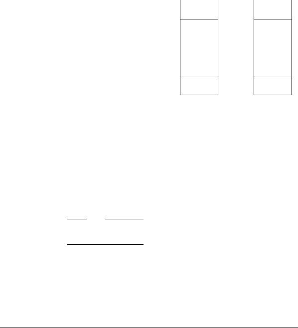
One possible memory map implementation is shown in Figure 2-40 on page 2-55. This shows the reset memory map with the boot code contained in bank 7 accessible at address 0x00000000. This memory can also be accessed at a higher address. This is required to allow the software to branch to this location prior to remapping the memory system. After remapping the memory system the RAM is available from bank 0. This is overlapped by a small internal RAM. This allows the vector code to be placed in the fast internal RAM and easy flow from internal to external memory in a continuous address space. This enables software to continue to execute without having to branch to a different location even if the code overflows the internal RAM without having to branch to a different location.
2-54 |
Copyright © 2001. All rights reserved. |
ARM DDI 0236A |
Functional Overview
Reset Memory |
Remap |
||
Map |
Memory Map |
||
|
|
|
|
Bank 7 ROM |
|
Bank 7 ROM |
|
|
|
|
|
Bank 7 ROM |
|
|
Bank 0 RAM |
|
|
|
|
|
|
|
0x00000000 |
|
|
|
|
|
Internal RAM |
|
Figure 2-40 Example memory map
2.5.2External bank SMCS7 size configuration
The SSMC allows the size of bank seven (selected with SMCS[7]) to be configured at reset using the external control pins SMMWCS7[1:0]. This feature is used to allow the boot memory size to be chosen at reset.
Bank seven can therefore always have the correct setting, and no additional software programming of the bank seven control register is required. However, the MW bits of SMBCR7 are still programmable, the same as the rest of the bank configuration registers. If you choose not to reconfigure the size of bank seven (by tying the pins to 11), then the bank size defaults to 8-bits.
Note
All other memory bank sizes have default settings that are set in the hardware, but can be programmed to the required values using software.
ARM DDI 0236A |
Copyright © 2001. All rights reserved. |
2-55 |

Functional Overview
The configuration of the bits used is shown in Table 2-11.
Table 2-11 External size configuration values for bank seven
SMMWCS7[1:0] |
Memory width |
|
|
00 |
8-bit |
|
|
01 |
16-bit |
|
|
10 |
32-bit |
|
|
11 |
No change |
|
|
Note
The control bit RBLE in the SMBCRx registers defaults to 0. This enables writes to 8-bit devices only. If other device widths are required then this bit must be set by software before the first write to the memory.
2-56 |
Copyright © 2001. All rights reserved. |
ARM DDI 0236A |