


CHAPTER 10
PULSE-WIDTH MODULATOR
The 8XC196EA has four pulse-width modulator (PWM) modules. Each module consists of an adjacent pair of PWM channels that can generate two PWM output signals with a fixed, programmable frequency and a variable duty cycle. These outputs can be used to drive motors that require an unfiltered PWM waveform for optimal efficiency, or they can be filtered to produce a smooth analog signal.
This chapter provides a functional overview of the pulse-width modulator module, describes how to program it, and provides sample circuitry for converting the PWM outputs to analog signals.
10.1 PWM FUNCTIONAL OVERVIEW
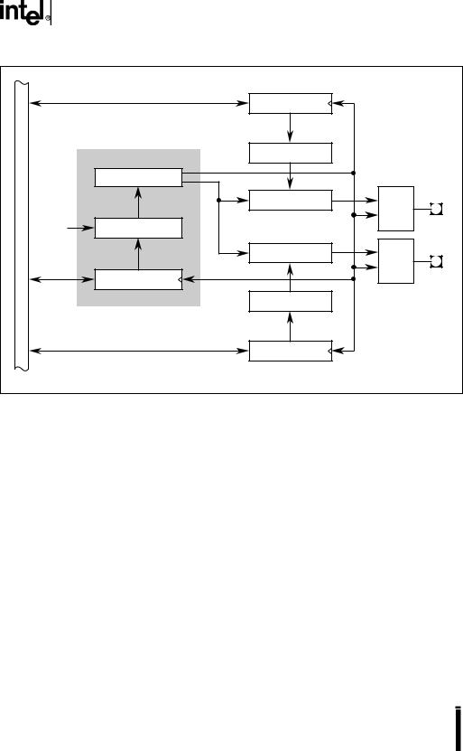
Each PWM module has two channels, each of which consists of a control register (PWM_CONTROL), a buffer, a comparator, an RS flip-flop, and an output pin. Three other components, an up counter, an eight-bit counter (PWMx_y_COUNT) and a period register (PWMx_y_PERIOD), are shared across the PWM module’s two channels, completing the circuitry (see Figure 10-1). Variables x and y represent the evenand odd-numbered members of an adjacent PWM channel pair, respectively.
10-1
8XC196EA USER’S MANUAL |
|
|
|
PWMx_CONTROL |
Reload |
|
|
|
|
|
Buffer |
|
Bufferx |
|
|
Count = 00H |
|
|
Up Counter |
|
|
Comparatorx |
R |
|
|
Q |
Internal |
|
S |
Clock |
PWMx_y_COUNT |
PWMx |
|
||
Signal |
|
|
Bus |
Comparatory |
R |
|
|
Q |
|
|
S |
|
PWMx_y_PERIOD |
PWMy |
|
|
|
|
Buffery |
|
|
|
Reload |
|
PWMy_CONTROL |
Buffer |
|
|
|
|
|
A3353-01 |
Figure 10-1. PWM Block Diagram
10.2 PWM SIGNALS AND REGISTERS
Table 10-1 describes the PWM’s signals and Table 10-2 briefly describes the control and status registers.
|
|
|
Table 10-1. PWM Signals |
||
Port Pin |
PWM |
PWM |
|
Description |
|
Signal |
Signal Type |
||||
|
|
||||
|
|
|
|
|
|
P11.0 |
PWM0 |
O |
|
Pulse-width modulator 0 output with high-drive capability. |
|
|
|
|
|
|
|
P11.1 |
PWM1 |
O |
|
Pulse-width modulator 1 output with high-drive capability. |
|
|
|
|
|
|
|
P11.2 |
PWM2 |
O |
|
Pulse-width modulator 2 output with high-drive capability. |
|
|
|
|
|
|
|
P11.3 |
PWM3 |
O |
|
Pulse-width modulator 3 output with high-drive capability. |
|
|
|
|
|
|
|
P11.4 |
PWM4 |
O |
|
Pulse-width modulator 4 output with high-drive capability. |
|
|
|
|
|
|
|
P11.5 |
PWM5 |
O |
|
Pulse-width modulator 5 output with high-drive capability. |
|
|
|
|
|
|
|
P11.6 |
PWM6 |
O |
|
Pulse-width modulator 6 output with high-drive capability. |
|
|
|
|
|
|
|
10-2

|
|
|
PULSE-WIDTH MODULATOR |
|
|
|
Table 10-1. PWM Signals (Continued) |
||
|
|
|
|
|
Port Pin |
PWM |
PWM |
Description |
|
Signal |
Signal Type |
|||
|
|
|||
|
|
|
|
|
P11.7 |
PWM7 |
O |
Pulse-width modulator 7 output with high-drive capability. |
|
|
|
|
|
|
Table 10-2. PWM Control and Status Registers
Mnemonic |
Address |
Description |
|
|
|
|
|
P11_DIR |
1FBAH |
Port Direction Register |
|
|
|
Each bit controls the configuration of the corresponding |
|
|
|
pin. Clearing a bit configures a pin as a complementary |
|
|
|
output; setting a bit configures a pin as a high-impedance |
|
|
|
input or an open-drain output. |
|
|
|
|
|
P11_MODE |
1FB8H |
Port Mode Register |
|
|
|
Each bit controls the mode of the corresponding pin. |
|
|
|
Setting a bit configures a pin as a special-function signal; |
|
|
|
clearing a bit configures a pin as a general-purpose I/O |
|
|
|
signal. |
|
|
|
|
|
P11_PIN |
1FBEH |
Port Pin Register |
|
|
|
Each bit reflects the current state of the corresponding |
|
|
|
pin, regardless of the pin’s mode and configuration. |
|
|
|
|
|
P11_REG |
1FBCH |
Port Data Output Register |
|
|
|
For I/O Mode (Px_MODE.x = 0) |
|
|
|
When a port pin is configured as a complementary |
|
|
|
output (Px_DIR.x = 0), setting the corresponding port |
|
|
|
data bit drives a one on the pin, and clearing the corre- |
|
|
|
sponding port data bit drives a zero on the pin. |
|
|
|
When a port pin is configured as a high-impedance |
|
|
|
input or an open-drain output (Px_DIR.x = 1), clearing |
|
|
|
the corresponding port data bit drives a zero on the |
|
|
|
pin, and setting the corresponding port data bit floats |
|
|
|
the pin, making it available as a high-impedance input. |
|
|
|
For Special-function Mode (Px_MODE.x = 1) |
|
|
|
When a port pin is configured as an output (either |
|
|
|
complementary or open-drain), the corresponding port |
|
|
|
data bit value is immaterial because the corresponding |
|
|
|
on-chip peripheral or system function controls the pin. |
|
|
|
To configure a pin as a high-impedance input, set both |
|
|
|
the Px_DIR and Px_REG bits. |
|
|
|
|
|
PWM0_CONTROL |
1EDEH |
PWM Duty Cycle |
|
PWM1_CONTROL |
1EDCH |
This register controls the PWM duty cycle. A zero loaded |
|
PWM2_CONTROL |
1EDAH |
||
into this register will cause the PWM to output a low |
|||
PWM3_CONTROL |
1ED8H |
||
continuously (0% duty cycle). An FFH in this register will |
|||
PWM4_CONTROL |
1ED6H |
||
cause the PWM to have its maximum duty cycle (99.6% |
|||
PWM5_CONTROL |
1ED4H |
||
duty cycle). |
|||
PWM6_CONTROL |
1ED2H |
||
|
|||
PWM7_CONTROL |
1ED0H |
|
|
|
|
|
10-3

8XC196EA USER’S MANUAL
Table 10-2. PWM Control and Status Registers (Continued)
Mnemonic |
Address |
Description |
|
|
|
|
|
PWM0_1_PERIOD |
1EDFH |
PWM Period |
|
PWM2_3_PERIOD |
1EDBH |
This register holds a programmed value that determines |
|
PWM4_5_PERIOD |
1ED7H |
||
the output period of a PWM output pair. The value is |
|||
PWM6_7_PERIOD |
1ED3H |
||
reloaded into the counter each time the counter resets to |
|||
|
|
||
|
|
00H. |
|
|
|
|
|
PWM0_1_COUNT |
1EDDH |
PWM Counter |
|
PWM2_3_COUNT |
1ED9H |
This read-only register contains the current value of the |
|
PWM4_5_COUNT |
1ED5H |
||
period counter. |
|||
PWM6_7_COUNT |
1ED1H |
||
|
|||
|
|
|
10.3 PWM OPERATION
The period register (PWMx_y_PERIOD) of each module controls the output frequency of both PWM outputs. Each control register (PWM_CONTROL) controls the duty cycle (the pulse width stated as a percentage of the period) of the corresponding PWM output. Each control register contains an eight-bit value that is loaded into a buffer when the eight-bit counter rolls over from FFH to 00H. The comparators compare the contents of the buffers to the counter value. Since the value written to the control register is buffered, you can write a new eight-bit value to either PWM_CONTROL register at any time. However, the comparators recognize the new value only after the current eight-bit count expires. The new value is used during the next PWM output period.
The counter continually increments until it rolls over to 00H, at which time the PWM output is driven high and the contents of the control registers are loaded into the buffers. The PWM output remains high until the counter value matches the value in the buffer, at which time the output is pulled low. You can read the count register (PWMx_y_COUNT) to see the current value of the counter. When the counter resets again (i.e., when an overflow occurs) the output is switched high. (Loading PWM_CONTROL with 00H forces the output to remain low.) Figure 10-2 shows typical PWM output waveforms.
10-4