

- •CONTENTS
- •FIGURES
- •TABLES
- •1.1 Manual Contents
- •1.2 Notational Conventions and Terminology
- •1.3 Related Documents
- •1.4 Application Support Services
- •2.1 Typical Applications
- •2.2 Microcontroller Features
- •2.3 Functional Overview
- •2.3.1 Core
- •2.3.1.3 Register File
- •2.3.2 Memory Controller
- •2.4 Internal Timing
- •2.4.1 Clock and Power Management Logic
- •2.4.2 Internal Timing
- •2.4.2.1 Clock Failure Detection Logic
- •2.4.2.2 External Timing
- •2.4.2.3 Power Management Options
- •2.4.3 Internal Memory
- •2.4.4 Serial Debug Unit
- •2.4.5 Interrupt Service
- •2.5 Internal Peripherals
- •2.5.1 I/O Ports
- •2.5.2 Serial I/O (SIO) Port
- •2.5.3 Synchronous Serial I/O (SSIO) Port
- •2.5.4 Event Processor Array (EPA) and Timer/Counters
- •2.5.7 Stack Overflow Module
- •2.5.8 Watchdog Timer
- •2.6 Special Operating Modes
- •2.7 Chip Configuration Registers
- •3.1 Overview of the Instruction Set
- •3.1.1 BIT Operands
- •3.1.2 BYTE Operands
- •3.1.4 WORD Operands
- •3.1.5 INTEGER Operands
- •3.1.9 Converting Operands
- •3.1.10 Conditional Jumps
- •3.1.11 Floating-Point Operations
- •3.1.12 Extended Instructions
- •3.2 Addressing Modes
- •3.2.1 Direct Addressing
- •3.2.2 Immediate Addressing
- •3.2.3 Indirect Addressing
- •3.2.3.1 Extended Indirect Addressing
- •3.2.3.2 Indirect Addressing with Autoincrement
- •3.2.3.3 Extended Indirect Addressing with Autoincrement
- •3.2.3.4 Indirect Addressing with the Stack Pointer
- •3.2.4 Indexed Addressing
- •3.2.4.3 Extended Indexed Addressing
- •3.2.4.4 Zero-indexed Addressing
- •3.3 Considerations for Crossing Page Boundaries
- •3.4 Software Protection Features and Guidelines
- •4.1 Memory Map Overview
- •4.2 Memory Partitions
- •4.2.1 External Memory
- •4.2.2 Internal ROM
- •4.2.2.1 Program Memory in Page FFH
- •4.2.2.3 Reserved Memory Locations
- •4.2.2.4 Interrupt, PIH, and PTS Vectors
- •4.2.2.5 Chip Configuration Bytes
- •4.2.3 Internal RAM (Code RAM)
- •4.2.4.2 Peripheral SFRs
- •4.2.5 Register File
- •4.2.5.2 Stack Pointer (SP)
- •4.3 Windowing
- •4.3.1 Selecting a Window
- •4.3.2 Addressing a Location Through a Window
- •4.3.2.4 Unsupported Locations Windowing Example
- •4.3.2.5 Using the Linker Locator to Set Up a Window
- •4.3.3 Windowing and Addressing Modes
- •4.4 Controlling Read Access to the Internal ROM
- •4.5 Remapping Internal ROM
- •5.1 Functional Overview
- •5.2 Stack Operations
- •5.3 Stack Overflow Module Registers
- •5.4 Programming the Stack Overflow Module
- •5.4.1 Initializing the Stack Pointer
- •5.4.2 Enabling the Stack Overflow Module and Specifying Stack Boundaries
- •6.1 Overview of the Interrupt Control Circuitry
- •6.2 Interrupt Signals and Registers
- •6.3 Interrupt Sources, Priorities, and Vector Addresses
- •6.3.1 PIH Interrupt Sources, Priorities, and Vector Addresses
- •6.3.1.1 Using Software to Provide the Vector Address
- •6.3.1.2 Providing the Vector Address in Response to a CPU Request
- •6.3.2 Special Interrupts
- •6.3.2.1 Unimplemented Opcode
- •6.3.2.2 Software Trap
- •6.3.2.4 Stack Overflow
- •6.3.3 External Interrupt Signal
- •6.3.4 Shared Interrupt Requests
- •6.4 Interrupt Latency
- •6.4.1 Situations that Increase Interrupt Latency
- •6.4.2 Calculating Latency
- •6.4.2.2 PTS Interrupt Latency
- •6.5 Programming the Interrupts
- •6.5.1 Modifying Interrupt Priorities
- •6.5.2 Determining the Source of an Interrupt
- •6.6 Initializing the PTS Control Blocks
- •6.6.1 Specifying the PTS Count
- •6.6.2 Selecting the PTS Mode
- •6.6.3 Single Transfer Mode
- •6.6.4 Block Transfer Mode
- •6.6.5 Dummy Mode
- •7.1 I/O Ports Overview
- •7.2 Configuring the Port Pins
- •7.2.2 Configuring Ports 3 and 4 (Address/Data Bus)
- •7.2.3 Port Configuration Example
- •7.3.1 Address and Data Signals (Ports 3, 4, and EPORT)
- •7.3.1.1 EPORT Status During Reset, CCB Fetch, Idle, Powerdown, and Hold
- •7.3.5 External Interrupt Signal (Port 2)
- •7.3.6 PWM Signals (Port 11)
- •7.3.7 Serial I/O Port Signals (Ports 2 and 7)
- •7.3.8 Special Operating Mode Signal (Port 5 Pin 7)
- •7.3.9 Synchronous Serial I/O Port Signals (Port 10)
- •7.4 I/O Port Internal Structures
- •7.4.3 Internal Structure for Ports 3 and 4 (Address/Data Bus)
- •8.1 Serial I/O (SIO) Port Functional Overview
- •8.2 Serial I/O Port Signals and Registers
- •8.3 Serial Port Modes
- •8.3.1 Synchronous Mode (Mode 0)
- •8.3.2 Asynchronous Modes (Modes 1, 2, and 3)
- •8.3.2.1 Mode 1
- •8.3.2.2 Mode 2
- •8.3.2.3 Mode 3
- •8.3.2.4 Multiprocessor Communications
- •8.4 Programming the Serial Port
- •8.4.1 Configuring the Serial Port Pins
- •8.4.2 Programming the Control Register
- •8.4.3 Programming the Baud Rate and Clock Source
- •8.4.4 Enabling the Serial Port Interrupts
- •8.4.5 Determining Serial Port Status
- •CHAPTER 9 Synchronous Serial I/O (SSIO) Port
- •9.1 SSIO Port Overview
- •9.1.1 Standard Mode
- •9.1.2 Duplex Mode
- •9.2 SSIO pORT sIGNALS AND rEGISTERS
- •9.3 ssio Port Operation
- •9.3.1 Transmitting and Receiving Data
- •9.3.1.1 Normal Transfers (All Modes)
- •9.3.1.2 Handshaking Transfers (Standard Mode Only)
- •9.4 Programming the SSIO Port
- •9.4.1 Configuring the SSIO Port Pins
- •9.4.2 Configuring the SSIO Registers
- •9.4.2.1 The SSIO Baud (SSIO_BAUD) Register
- •9.4.2.3 The SSIO 0 Clock (SSIO0_CLK) Register
- •9.4.2.4 The SSIO 1 Clock (SSIO1_CLK) Register
- •9.4.3 Enabling the SSIO Interrupts
- •9.5 Programming Considerations
- •9.5.2 Standard Mode Considerations
- •9.5.3 Duplex Mode Considerations
- •10.1 PWM FUNCTIONAL OVERVIEW
- •10.2 PWM Signals and Registers
- •10.3 pwm operation
- •10.4 Programming the Frequency and Period
- •10.5 Programming the Duty Cycle
- •10.5.1 Sample Calculations
- •10.5.2 Reading the Current Value of the Down-counter
- •10.5.3 Enabling the PWM Outputs
- •10.5.4 Generating Analog Outputs
- •11.1 EPA Functional Overview
- •11.2 EPA and Timer/Counter Signals and Registers
- •11.3 Timer/Counter Functional Overview
- •11.3.1 Timer Multiplexing on the Time Bus
- •11.4 EPA Channel Functional Overview
- •11.4.1 Operating in Input Capture Mode
- •11.4.2 Operating in Output Compare Mode
- •11.4.3 Operating in Compare Mode with the Output/Simulcapture Channels
- •11.4.4 Generating a 32-bit Time Value
- •11.4.5 Controlling a Pair of Adjacent Pins
- •11.5 Programming the EPA and Timer/Counters
- •11.5.1 Configuring the EPA and Timer/Counter Signals
- •11.5.2 Programming the Timers
- •11.5.3 Programming the Capture/Compare Channels
- •11.5.4 Programming the Compare-only (Output/Simulcapture) Channels
- •11.6 Enabling the EPA Interrupts
- •11.7 Determining Event Status
- •CHAPTER 12 Analog-to-digital (A/D) Converter
- •12.1 A/D Converter Functional Overview
- •12.2 A/D Converter Signals and Registers
- •12.3 A/D Converter Operation
- •12.4 Programming the A/D Converter
- •12.4.1 Programming the A/D Test Register
- •12.4.2 Programming the A/D Result Register (for Threshold Detection Only)
- •12.4.3 Programming the A/D Time Register
- •12.4.4 Programming the A/D Command Register
- •12.4.5 Programming the A/D Scan Register
- •12.4.6 Enabling the A/D Interrupt
- •12.5 Determining A/D Status and Conversion Results
- •12.6 Design Considerations
- •12.6.1 Designing External Interface Circuitry
- •12.6.1.1 Minimizing the Effect of High Input Source Resistance
- •12.6.1.2 Suggested A/D Input Circuit
- •12.6.1.3 Analog Ground and Reference Voltages
- •12.6.2 Understanding A/D Conversion Errors
- •CHAPTER 13 Minimum Hardware Considerations
- •13.1 Minimum Connections
- •13.1.1 Unused Inputs
- •13.1.2 I/O Port Pin Connections
- •13.2 Applying and Removing Power
- •13.3 Noise Protection Tips
- •13.4 The On-chip Oscillator Circuitry
- •13.5 Using an External Clock Source
- •13.6 Resetting the Microcontroller
- •13.6.1 Generating an External Reset
- •13.6.2 Issuing the Reset (RST) Instruction
- •13.6.3 Issuing an Illegal IDLPD Key Operand
- •13.6.4 Enabling the Watchdog Timer
- •13.6.5 Detecting Clock Failure
- •13.7 Identifying the Reset Source
- •14.1 Special Operating Mode Signals and Registers
- •14.2 Reducing Power Consumption
- •14.3 Idle Mode
- •14.3.1 Enabling and Disabling Idle Mode
- •14.3.2 Entering and Exiting Idle Mode
- •14.4 Powerdown Mode
- •14.4.1 Enabling and Disabling Powerdown Mode
- •14.4.2 Entering Powerdown Mode
- •14.4.3 Exiting Powerdown Mode
- •14.4.3.1 Generating a Hardware Reset
- •14.4.3.2 Asserting the External Interrupt Signal
- •14.4.3.3 Selecting an External Capacitor
- •14.5 ONCE Mode
- •CHAPTER 15 Interfacing with External Memory
- •15.1 Internal and External Addresses
- •15.2 External Memory Interface Signals and Registers
- •15.3 The Chip-select Unit
- •15.3.1 Defining Chip-select Address Ranges
- •15.3.2 Controlling Bus Parameters
- •15.3.3 Chip-select Unit Initial Conditions
- •15.3.4 Programming the Chip-select Registers
- •15.3.5 Example of a Chip-select Setup
- •15.4 Chip Configuration Registers and Chip Configuration Bytes
- •15.5 Bus Width and Multiplexing
- •15.5.1 A 16-bit Example System
- •15.5.2 16-bit Bus Timings
- •15.5.3 8-bit Bus Timings
- •15.5.4 Comparison of Multiplexed and Demultiplexed Buses
- •15.6 Wait States (Ready Control)
- •15.7 Bus-hold Protocol
- •15.7.1 Enabling the Bus-hold Protocol
- •15.7.2 Disabling the Bus-hold Protocol
- •15.7.3 Hold Latency
- •15.7.4 Regaining Bus Control
- •15.8 Write-control Modes
- •15.9 System Bus AC Timing Specifications
- •15.9.1 Deferred Bus-cycle Mode
- •15.9.2 Explanation of AC Symbols
- •15.9.3 AC Timing Definitions
- •16.1 Serial Debug Unit (SDU) Functional Overview
- •16.2 SDU Signals and Registers
- •16.3 SDU Operation
- •16.3.1 SDU State Machine
- •16.3.2 Code RAM Access State Machine
- •16.3.3 Minimizing Latency
- •16.4 Code RAM Access
- •16.4.1 Code RAM Data Transfer
- •16.4.2 Code RAM Access Instructions
- •16.4.3 Code RAM Data Transfer Example
- •16.5 SDU Interface Connector
- •17.1 Signals and Registers
- •17.2 Memory Protection Options
- •17.3 Entering Test-ROM Routines
- •17.3.1 Power-up and Power-down Sequences
- •17.4 ROM-dump Routine and Circuit
- •17.5 Serial Port Mode Routine
- •17.5.1 Serial Port RISM
- •17.5.2 Serial Port Mode Circuit
- •17.6 SDU RISM Execution Routine
- •17.6.1 SDU RISM Data Transfer
- •17.6.1.1 SDU RISM Data Transfer Before
- •17.6.1.2 SDU RISM Data Transfer After
- •17.6.2 SDU RISM Execution Circuit
- •17.7 RISM Command Descriptions
- •17.8 Executing Programs from Register RAM
- •17.9 RISM Command Examples
- •17.9.1 Serial Port Mode RISM Read Command Example
- •17.9.2 Serial Port Mode RISM Write Command Example
- •17.9.3 SDU RISM Execution Write Command Example
- •17.9.4 SDU RISM Execution Go Command Example
- •B.1 Functional Groupings of Signals
- •B.2 Signal Descriptions
- •B.3 Default Conditions
8XC196EA USER’S MANUAL
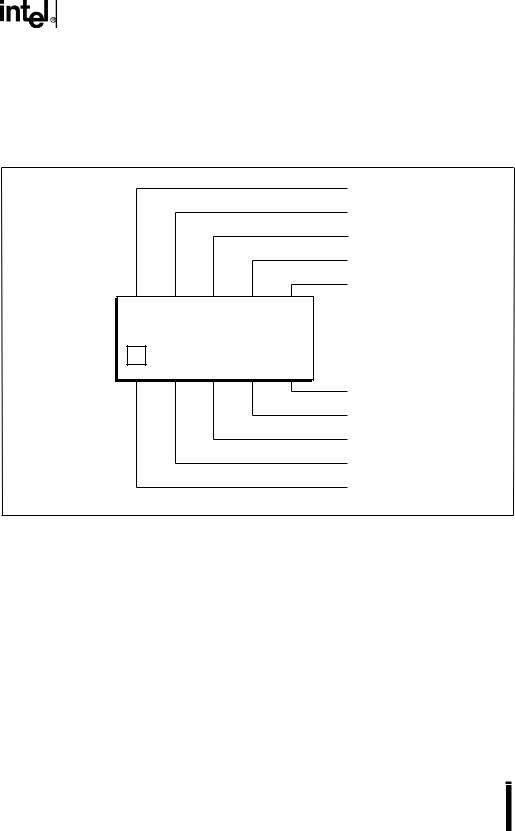
16.5 SDU INTERFACE CONNECTOR
To standardize the connector interface to the SDU port, we recommend that you use a 10-pin, 2- row I/O expansion connector. This low cost, readily available standard connector can be easily added to any printed-circuit board (PCB) after manufacturing of the module.
Figure 16-11 describes the SDU port connector pinout.
No Connect
CRDCLK
CRBUSY#
CRIN
CROUT
2 |
4 |
6 |
8 |
10 |
||||
|
|
|
|
|
|
|
|
|
|
|
|
|
|
|
|
|
|
|
|
|
|
|
|
|
|
|
1 |
3 |
5 |
7 |
9 |
Vcc
RESET#
Vss
Vss
Key (No Connect)
A4306-01
Figure 16-11. SDU Interface Connector
To prevent mis-socketing and ensure proper cable connection, we recommend that you remove the square pin at position #1 (Key) and block the adjoining cable position.
16-14
17
Using the Test-ROM
Routines

CHAPTER 17
USING THE TEST-ROM ROUTINES
Within the memory array of the 8XC196EA resides 1 Kbyte of nonerasable memory, commonly referred to as test-ROM. Embedded in the test-ROM are three software routines: ROM-dump, serial port, and serial debug unit (SDU) RISM execution. These routines enable you to perform the following operations:
•Use the ROM-dump routine to write the entire ROM array to an external memory device to verify its contents.
•Use the serial port routine to download code and data (usually from a personal computer or workstation) to a microcontroller (the slave) through the serial I/O port.
•Use the SDU RISM execution routine to download code and data across a high-speed dedicated serial link.
17.1 SIGNALS AND REGISTERS
Table 17-1 describes the signals used in test-mode entry, and Figure 17-1 describes chip configuration register 0 (CCR0), which controls access to the ROM. Several pins combine to control entry into these modes, and three port 12 pins (P12.2:0) select the desired test-ROM routine. The serial port mode and ROM-dump routines configure additional pins, which are required to execute properly.
Table 17-1. Signal Descriptions
Port |
Special-function |
Typ |
Mode |
|
|
|
Description |
Pin |
Signal |
e |
|
|
|
||
|
|
|
|
|
|||
|
|
|
|
|
|||
P12.2:0 |
— |
I |
All |
Test-ROM Routine Select † |
|||
|
|
|
|
Determines the test-ROM routine. These pins are |
|||
|
|
|
|
sampled after a device reset and must be static while |
|||
|
|
|
|
the part is operating. |
|||
|
|
|
|
P12.2 |
P12.1 |
P12.0 |
|
|
|
|
|
0 |
0 |
0 |
Serial port mode |
|
|
|
|
1 |
0 |
0 |
ROM-dump |
|
|
|
|
1 |
1 |
1 |
SDU RISM execution |
|
|
|
|
† All other pin combinations are reserved. |
|||
P2.0 |
TXD0 |
O |
Serial |
Transmit Serial Data 0 |
|||
|
|
|
|
During serial port mode, TXD0 transmits data to an |
|||
|
|
|
|
external device. |
|
||
|
|
|
|
|
|||
P2.1 |
RXD0 |
I |
Serial |
Receive Serial Data 0 |
|||
|
|
|
|
During serial port mode, RXD0 receives data from an |
|||
|
|
|
|
external device. |
|
||
|
|
|
|
|
|
|
|
17-1