


University Program UP2 Education Kit User Guide
3.Select the first target device name in the Device Name list in the
Multi-Device JTAG Chain Setup dialog box.
4.Type the name of the programming file for the device listed in the
Device Name box in the Programming File Names box. The Select Programming File button can also be used to browse your computer’s directory structure to locate the appropriate programming file.
5.Click Add to add the device and associated programming file to the
Device Names & Programming File Names box. The number to the left of the device name shows the device’s order in the JTAG chain. The device’s associated programming file is displayed on the same line as the device name. If no programming file is associated with a device, “<none>” is displayed next to the device name.
6.Repeat steps 3 through 5 to add information for each device in the JTAG chain.
7.Click Detect JTAG Chain Info to have the ByteBlaster II cable check the device count, JTAG ID code, and total instruction length of the multi-device JTAG chain. A message just above the Detect JTAG Chain Info button reports the information detected by the ByteBlaster II cable. You must manually verify that this message matches the information in the Device Names & Programming File Names box.
8.Click Save JCF to save the current settings to a JCF for future use. Type the name of the file in the File Name box and then select the desired directory in the Directories box. Click OK.
9.Click OK to save the changes.
10.Click Configure in the Quartus II Programmer to configure all FLEX 10K devices in the JTAG chain. Then, click Program to program all EPM7128S devices in the JTAG chain.
Connect Multiple UP2 Education Boards Together in a Chain
This section describes the procedures for connecting multiple UP2 Education Boards together (i.e., how to set the on-board jumpers, connect the ByteBlaster II download cable, and set options in the Quartus II software).
Altera Corporation |
23 |

University Program UP2 Education Kit User Guide
Setting the On-Board Jumpers for Connecting Multiple UP2 Education Boards Together
To configure/program EPM7128S and FLEX 10K devices on multiple UP2 Education Boards connected in a multi-device JTAG chain, set the jumpers TDI, TDO, DEVICE, and BOARD for all boards except the last board in the chain as shown in Figure 10.
Figure 10. Jumper Settings for All Boards Except the Last Board in the Chain
TDI TDO DEVICE BOARD
C1 |
C1 |
C1 |
C1 |
C2 |
C2 |
C2 |
C2 |
C3 |
C3 |
C3 |
C3 |
The last UP2 Education Board in the chain can configure and program one or both devices. However, the BOARD jumper must be set as shown in Figure 11.
Figure 11. Jumper Settings for the Last Board in the Chain
The TDI, TDO, and DEVICE settings depend on which configuration is used.
TDI TDO DEVICE BOARD
C1 |
C1 |
C1 |
C1 |
C2 |
C2 |
C2 |
C2 |
C3 |
C3 |
C3 |
C3 |
Connecting the ByteBlaster II Download Cable for Connecting Multiple UP2 Education Boards Together
Attach the ByteBlaster II cable directly to your PC’s parallel port and to the JTAG_IN connector on the UP2 Education Board.
f For more information on setting up the ByteBlaster II cable, see the
ByteBlaster II Parallel Port Download Cable Data Sheet.
24 |
Altera Corporation |

University Program UP2 Education Kit User Guide
VGA Driver
Operation
Setting the JTAG Options in the Quartus II Software for Connecting Multiple UP2 Education Boards
For information on how to set the JTAG options in the Quartus II software, see “Setting the JTAG Options in the Quartus II Software for Configuring & Programming Both Devices” on page 22.
A standard VGA monitor consists of a grid of pixels that can be divided into rows and columns. A VGA monitor contains at least 480 rows, with 640 pixels per row, as shown in Figure 12. Each pixel can display various colors, depending on the state of the red, green, and blue signals.
Figure 12. VGA Monitor
640 pixels
(0,0)
480 pixels
(640, 480)
Each VGA monitor has an internal clock that determines when each pixel is updated. This clock operates at the VGA-specified frequency of 25.175 MHz. The monitor refreshes the screen in a prescribed manner that is partially controlled by the horizontal and vertical synchronization signals. The monitor starts each refresh cycle by updating the pixel in the top left-hand corner of the screen, which can be treated as the origin of an X–Y plane (see Figure 12). After the first pixel is refreshed, the monitor refreshes the remaining pixels in the row. When the monitor receives a pulse on the horizontal synchronization, it refreshes the next row of pixels. This process is repeated until the monitor reaches the bottom of the screen. When the monitor reaches the bottom of the screen, the vertical synchronization pulses, causing the monitor to begin refreshing pixels at the top of the screen (i.e., at [0,0]).
VGA Timing
For the VGA monitor to work properly, it must receive data at specific times with specific pulses. Horizontal and vertical synchronization pulses must occur at specified times to synchronize the monitor while it is
Altera Corporation |
25 |

University Program UP2 Education Kit User Guide
receiving color data. Figures 13 and 14 show the timing waveforms for the color information with respect to the horizontal and vertical synchronization signals.
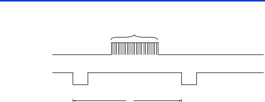
Figure 13. Horizontal Refresh Cycle
RED, GREEN, BLUE

 C
C 

 D
D 

 E
E 

HORIZ_SYNC

 B
B 

A
Parameters |
A |
B |
C |
D |
E |
|
|
|
|
|
|
Time |
31.77 s |
3.77 s |
1.89 s |
25.17 s |
0.94 s |
|
|
|
|
|
|
26 |
Altera Corporation |
University Program UP2 Education Kit User Guide
Figure 14. Vertical Refresh Cycle
480 Horizontal
Refresh Cycles
RED, GREEN, BLUE

 Q
Q 

 R
R 

 S
S 

VERT_SYNC
 P
P 

O
Parameters |
O |
P |
Q |
R |
S |
|
|
|
|
|
|
Time |
16.6 ms |
64 s |
1.02 ms |
15.25 ms |
0.35 ms |
|
|
|
|
|
|
|
|
|
|
|
|
The frequency of operation and the number of pixels that the monitor must update determines the time required to update each pixel, and the time required to update the whole screen. The following equations roughly calculate the time required for the monitor to perform all of its functions.
Tpixel |
= |
1/fCLK = 40 ns |
TROW |
= |
A = B + C + D + E |
|
= |
(Tpixel × 640 pixels) + row + guard bands = 31.77 µs |
Tscreen |
= |
O = P + Q + R + S |
|
= |
(TROW × 480 rows) + guard bands = 16.6 ms |
Where: Tpixel |
= Time required to update a pixel |
|
fCLK |
= |
25.175 MHz |
TROW |
= Time required to update one row |
|
Tscreen |
= Time required to update the screen |
|
B, C, E |
= |
Guard bands |
P, Q, S |
= |
Guard bands |
The monitor writes to the screen by sending red, green, blue, horizontal synchronization, and vertical synchronization signals when the screen is at the expected location. Once the timing of the horizontal and vertical synchronization signals is accurate, the monitor only needs to keep track of the current location, so it can send the correct color data to the pixel.
Altera Corporation |
27 |

University Program UP2 Education Kit User Guide
Mouse
Interface
Operation
You can connect a mouse to the UP2 Education Board via the 6-pin mini-DIN connector. The data is sent using a synchronous serial protocol, and the transmission is controlled by the CLK and DATA signals. During non-transmission, CLK is at logic 1 and DATA can be either logic 0 or logic 1.
Each transmission contains one start bit, eight data bits, odd parity, and one stop bit. Data transmission starts from the least significant bit (LSB), (i.e., the sequence of transmission is start bit, DATA0 through DATA7, parity, and stop bit). Start bits are logic 0, and stop bits are logic 1. Each clock period is 30 to 50 µsec; the data transition to the falling edge of the clock is 5 to 25 µsec. Table 13 shows the data packet format.
Table 13. Data Packet Format |
Note (1) |
|
|
|
|
|
|||
|
|
|
|
|
|
|
|
|
|
Packet |
D7 |
D6 |
|
D5 |
D4 |
D3 |
D2 |
D1 |
D0 |
Number |
|
|
|
|
|
|
|
|
|
|
|
|
|
|
|
|
|
|
|
1 |
YV |
XV |
|
YS |
XS |
1 |
0 |
R |
L |
|
|
|
|
|
|
|
|
|
|
2 |
X7 |
X6 |
|
X5 |
X4 |
X3 |
X2 |
X1 |
X0 |
|
|
|
|
|
|
|
|
|
|
3 |
Y7 |
Y6 |
|
Y5 |
Y4 |
Y3 |
Y2 |
Y1 |
Y0 |
|
|
|
|
|
|
|
|
|
|
Note to Table 13:
(1)Where: L = Left button state (1 = left mouse button is pressed down)
R |
= Right button state (1 = right mouse button is pressed down) |
|
X0 – X7 |
= Movement in X direction |
|
Y0 – Y7 |
= Movement in Y direction |
|
XS, YS |
= |
Movement data sign (1 = negative) |
XV, YV |
= |
Movement data overflow (1 = overflow has occurred) |
The mouse operates on a Cartesian coordinate system (i.e., moving to the right is positive, moving to the left is negative, moving up is positive, and moving down is negative). The magnitude of the movement is a function of the mouse’s rate of movement. The faster the mouse moves, the greater the magnitude.
28 |
Altera Corporation |

Notes:
Altera Corporation |
29 |

University Program UP2 Education Kit User Guide
 ®
®
101 Innovation Drive San Jose, CA 95134 (408) 544-7000 http://www.altera.com University Program: university@altera.com Literature Services: (888) 3-ALTERA lit_req@altera.com
30
Printed on Recycled Paper.
Altera, MAX II, MAX 7000S, Quartus II, EPM7128S, FLEX, FLEX 10K, EPF10K20, EPF10K70, ByteBlaster II, EPC1, and AHDL are trademarks and/or service marks of Altera Corporation in the United States and other countries. Altera acknowledges the trademarks of other organizations for their respective products or services mentioned in this document. Altera products are protected under numerous U.S. and foreign patents and pending applications, maskwork rights, and copyrights. Altera warrants performance of its semiconductor products to current specifications in accordance with Altera’s standard warranty, but reserves the right to make changes to any products and services at any time without notice. Altera assumes no responsibility or liability arising out of the application or use of any information, product, or service
described herein except as expressly agreed to in writing by Altera Corporation. Altera customers are advised to obtain the latest version of device specifications before relying on any published information and before placing orders for products or services.
Copyright ♥ 2004 Altera Corporation. All rights reserved.
Altera Corporation